EP1533854A2 - Organischer Dünnfilmtransistor mit einer Pufferschicht - Google Patents
Organischer Dünnfilmtransistor mit einer Pufferschicht Download PDFInfo
- Publication number
- EP1533854A2 EP1533854A2 EP04256994A EP04256994A EP1533854A2 EP 1533854 A2 EP1533854 A2 EP 1533854A2 EP 04256994 A EP04256994 A EP 04256994A EP 04256994 A EP04256994 A EP 04256994A EP 1533854 A2 EP1533854 A2 EP 1533854A2
- Authority
- EP
- European Patent Office
- Prior art keywords
- thin film
- film transistor
- organic thin
- organic
- protective layer
- Prior art date
- Legal status (The legal status is an assumption and is not a legal conclusion. Google has not performed a legal analysis and makes no representation as to the accuracy of the status listed.)
- Withdrawn
Links
Images


Classifications
-
- H—ELECTRICITY
- H10—SEMICONDUCTOR DEVICES; ELECTRIC SOLID-STATE DEVICES NOT OTHERWISE PROVIDED FOR
- H10D—INORGANIC ELECTRIC SEMICONDUCTOR DEVICES
- H10D30/00—Field-effect transistors [FET]
- H10D30/60—Insulated-gate field-effect transistors [IGFET]
- H10D30/67—Thin-film transistors [TFT]
-
- H—ELECTRICITY
- H10—SEMICONDUCTOR DEVICES; ELECTRIC SOLID-STATE DEVICES NOT OTHERWISE PROVIDED FOR
- H10K—ORGANIC ELECTRIC SOLID-STATE DEVICES
- H10K10/00—Organic devices specially adapted for rectifying, amplifying, oscillating or switching; Organic capacitors or resistors having potential barriers
- H10K10/40—Organic transistors
- H10K10/46—Field-effect transistors, e.g. organic thin-film transistors [OTFT]
- H10K10/462—Insulated gate field-effect transistors [IGFETs]
- H10K10/468—Insulated gate field-effect transistors [IGFETs] characterised by the gate dielectrics
- H10K10/471—Insulated gate field-effect transistors [IGFETs] characterised by the gate dielectrics the gate dielectric comprising only organic materials
-
- H—ELECTRICITY
- H10—SEMICONDUCTOR DEVICES; ELECTRIC SOLID-STATE DEVICES NOT OTHERWISE PROVIDED FOR
- H10K—ORGANIC ELECTRIC SOLID-STATE DEVICES
- H10K10/00—Organic devices specially adapted for rectifying, amplifying, oscillating or switching; Organic capacitors or resistors having potential barriers
- H10K10/40—Organic transistors
- H10K10/46—Field-effect transistors, e.g. organic thin-film transistors [OTFT]
- H10K10/462—Insulated gate field-effect transistors [IGFETs]
- H10K10/466—Lateral bottom-gate IGFETs comprising only a single gate
-
- H—ELECTRICITY
- H10—SEMICONDUCTOR DEVICES; ELECTRIC SOLID-STATE DEVICES NOT OTHERWISE PROVIDED FOR
- H10K—ORGANIC ELECTRIC SOLID-STATE DEVICES
- H10K10/00—Organic devices specially adapted for rectifying, amplifying, oscillating or switching; Organic capacitors or resistors having potential barriers
- H10K10/80—Constructional details
-
- H—ELECTRICITY
- H10—SEMICONDUCTOR DEVICES; ELECTRIC SOLID-STATE DEVICES NOT OTHERWISE PROVIDED FOR
- H10K—ORGANIC ELECTRIC SOLID-STATE DEVICES
- H10K77/00—Constructional details of devices covered by this subclass and not covered by groups H10K10/80, H10K30/80, H10K50/80 or H10K59/80
- H10K77/10—Substrates, e.g. flexible substrates
- H10K77/111—Flexible substrates
-
- H—ELECTRICITY
- H10—SEMICONDUCTOR DEVICES; ELECTRIC SOLID-STATE DEVICES NOT OTHERWISE PROVIDED FOR
- H10K—ORGANIC ELECTRIC SOLID-STATE DEVICES
- H10K50/00—Organic light-emitting devices
- H10K50/80—Constructional details
- H10K50/84—Passivation; Containers; Encapsulations
-
- H—ELECTRICITY
- H10—SEMICONDUCTOR DEVICES; ELECTRIC SOLID-STATE DEVICES NOT OTHERWISE PROVIDED FOR
- H10K—ORGANIC ELECTRIC SOLID-STATE DEVICES
- H10K85/00—Organic materials used in the body or electrodes of devices covered by this subclass
- H10K85/30—Coordination compounds
- H10K85/321—Metal complexes comprising a group IIIA element, e.g. Tris (8-hydroxyquinoline) gallium [Gaq3]
- H10K85/324—Metal complexes comprising a group IIIA element, e.g. Tris (8-hydroxyquinoline) gallium [Gaq3] comprising aluminium, e.g. Alq3
-
- H—ELECTRICITY
- H10—SEMICONDUCTOR DEVICES; ELECTRIC SOLID-STATE DEVICES NOT OTHERWISE PROVIDED FOR
- H10K—ORGANIC ELECTRIC SOLID-STATE DEVICES
- H10K85/00—Organic materials used in the body or electrodes of devices covered by this subclass
- H10K85/60—Organic compounds having low molecular weight
- H10K85/615—Polycyclic condensed aromatic hydrocarbons, e.g. anthracene
- H10K85/621—Aromatic anhydride or imide compounds, e.g. perylene tetra-carboxylic dianhydride or perylene tetracarboxylic di-imide
-
- Y—GENERAL TAGGING OF NEW TECHNOLOGICAL DEVELOPMENTS; GENERAL TAGGING OF CROSS-SECTIONAL TECHNOLOGIES SPANNING OVER SEVERAL SECTIONS OF THE IPC; TECHNICAL SUBJECTS COVERED BY FORMER USPC CROSS-REFERENCE ART COLLECTIONS [XRACs] AND DIGESTS
- Y02—TECHNOLOGIES OR APPLICATIONS FOR MITIGATION OR ADAPTATION AGAINST CLIMATE CHANGE
- Y02E—REDUCTION OF GREENHOUSE GAS [GHG] EMISSIONS, RELATED TO ENERGY GENERATION, TRANSMISSION OR DISTRIBUTION
- Y02E10/00—Energy generation through renewable energy sources
- Y02E10/50—Photovoltaic [PV] energy
- Y02E10/549—Organic PV cells
-
- Y—GENERAL TAGGING OF NEW TECHNOLOGICAL DEVELOPMENTS; GENERAL TAGGING OF CROSS-SECTIONAL TECHNOLOGIES SPANNING OVER SEVERAL SECTIONS OF THE IPC; TECHNICAL SUBJECTS COVERED BY FORMER USPC CROSS-REFERENCE ART COLLECTIONS [XRACs] AND DIGESTS
- Y02—TECHNOLOGIES OR APPLICATIONS FOR MITIGATION OR ADAPTATION AGAINST CLIMATE CHANGE
- Y02P—CLIMATE CHANGE MITIGATION TECHNOLOGIES IN THE PRODUCTION OR PROCESSING OF GOODS
- Y02P70/00—Climate change mitigation technologies in the production process for final industrial or consumer products
- Y02P70/50—Manufacturing or production processes characterised by the final manufactured product
Definitions
- the present invention relates to an organic thin film transistor comprising a buffer layer, and more particularly to an organic thin film transistor comprising a substrate, a gate electrode, a gate insulating layer, an organic semiconductor layer, source-drain electrodes and a protective layer.
- a buffer layer is interposed between the organic semiconductor layer and the protective layer, thereby minimizing the deterioration in the performance of the transistor caused by ambient air containing oxygen and moisture, and mounting process of a display device thereto.
- a device using an organic thin film transistor necessitates a protective layer for protecting the transistor from ambient air containing oxygen and moisture, and a supporting layer for mounting a display device, particularly in the case of a display application.
- Some attempts to form an inorganic film made of SiN x , SiO x , etc. on an organic thin film transistor by CVD or sputtering have been made, but the processes cause serious deterioration of the organic semiconductor layer due to active gases or plasma. This results in drastic reduction in the performance of the organic thin film transistor.
- a feature of the present invention is to provide an organic thin film transistor wherein a buffer layer is interposed between an organic semiconductor layer and a protective layer so that the buffer layer prevents the deterioration of the organic semiconductor layer by a material used to form the protective layer and minimizes the degeneration in the performance of the transistor after formation of the protective layer.
- an organic thin film transistor comprising a substrate, a gate electrode, a gate insulating layer, an organic semiconductor layer, source-drain electrodes and a protective layer wherein a buffer layer is interposed between the organic semiconductor layer and the protective layer.
- Figs. 1a and 1b are cross-sectional views showing structures of organic thin film transistors according to the present invention.
- the organic thin film transistor of the present invention comprises a substrate 1, a gate electrode 2, a gate insulating layer 3, source-drain electrodes 4, an organic semiconductor layer 5, a buffer layer 6, a first protective layer 7 and a second protective layer 8, and the buffer layer 6 is interposed between the organic semiconductor layer 5 and the first protective layer 7.
- the structures of the organic thin film transistor shown in Figs. 1a and 1b are simply preferred embodiments, and it is to be understood that various structures of the organic thin film transistor comprising the buffer layer and the protective layer are possible so far as they do not detract from the object of the present invention.
- the buffer layer is made of an organic material having a resistance of 10 6 ohm-cm more.
- organic material include, but are not limited to, Alq3 (tris(8-hydroxyquinoline)aluminum), BAlq3 (bis(2-methyl-8-quinolato)(p-phenyl-phenolato)aluminum), PTCDA (perylenetetracarboxylicdianhydride), DPS (dicyano substituted diphenylsulfone), TCNQ (tetracyano-quinodimethane), DCAQ (2-tert-butyl-9,10-N,N'-dicyanoanthraquinonediimine) and the like.
- the buffer layer may be formed by a variety of techniques including vacuum deposition, dip coating, spin coating, printing, spray coating, roll coating, etc.
- the protective layer preferably has a double-layer structure of a first protective layer and a second protective layer as shown in Figs. 1a and 1b.
- the first protective layer is made of a water-soluble organic material such as PVA (polyvinyl alcohol), and the second protective layer is made of an organic material crosslinkable by UV light or heat such as a photoactive or thermoactive polyacrylate.
- the structure of the protective layer is not specifically limited to the structure described herein, and various structures are possible.
- Materials for the gate insulating layer of the organic thin film transistor according to the present invention include, but are not limited to, polyolefins, polyvinyls, polyacrylates, polystyrenes, polyurethanes, polyimides and derivatives thereof.
- materials for the organic semiconductor layer materials commonly used in the art can be used. Specific examples of the materials include, but are not limited to, pentacenes, copper phthalocyanines, polythiophenes, polyanilines, polyacetylenes, polypyrroles, polyphenylene vinylenes and derivatives thereof.
- metals and conductive polymers commonly used in the art can be used.
- specific examples of the materials include, but are not limited to, gold (Au), silver (Ag), aluminum (Al), nickel (Ni), indium-tin oxides (ITOs), polythiophenes, polyanilines, polyacetylenes, polypyrroles, polyphenylene vinylenes, PEDOT(polyethylenedioxythiophene)/PSS(polystyrenesulfonate) mixtures and the like.
- materials for the substrate of the organic thin film transistor according to the present invention include, but are not limited to, glass, silicone, plastics and the like.
- Example 1 Fabrication of organic thin film transistor comprising buffer layer and protective layer
- an organic thin film transistor having the structure shown in Fig. 1a was fabricated.
- Al was deposited on a washed glass substrate by a vacuum deposition technique to form a gate electrode with a thickness of 1,500 ⁇ .
- a mixture of a polyimide-based material and a polyacrylate-based material was coated onto the gate electrode to a thickness of 7,000 ⁇ by a spin coating at 2,000rpm.
- the coating was baked at 100°C for 10 minutes and 150°C for 2 hours, sequentially, to form an organic gate insulating layer.
- OMBD organic molecular beam deposition
- a vacuum pressure of 2x10 -7 torr a substrate temperature of 50°C and a deposition rate of 0.85 ⁇ /sec.
- gold was deposited on the organic semiconductor layer through a shadow mask having a channel length of 100 ⁇ m and a channel width of 0.5mm to form source-drain electrodes with a thickness of 1,000 ⁇ .
- Alq3 was deposited to a thickness 1,000 ⁇ at a substrate temperature of 30°C and a deposition rate of 1 ⁇ /sec.
- a first protective layer was formed by spin coating PVA on the buffer layer to a thickness of 300 ⁇ by spin coating, followed by drying it in a convection oven at 100°C for 10 minutes. Thereafter, a second protective layer was formed by spin coating PR (PC-403, JSR) to a thickness of 2 ⁇ m.
- the formed protective layer was soft-baked in a convection oven at 100°C for 2 minutes, exposed to light for 20 seconds, and then hard-baked on a hot plate at 100°C for 1 hour to fabricate an organic thin film transistor.
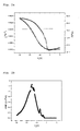
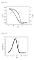
- Curves showing the current transfer characteristics and the charge carrier mobility of the device before formation of the protective layer were plotted using a KEITHLEY semiconductor characterization system (4200-SCS), and are shown in Figs. 2a and 2b, respectively. Curves showing the current transfer characteristics and the charge carrier mobility of the final device in which the protective layer was formed were plotted using the same system and are shown in Figs. 3a and 3b, respectively.
- the current ratio I on /I off decreases. Accordingly, the kind and the thickness of the dielectric film are important factors in determining the current ratio. In this case, the off-state leakage current becomes low.
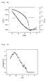
- An organic thin film transistor was fabricated in the same manner as in Example 1 above, except that a buffer layer was not formed.
- Curves showing the current transfer characteristics and the charge carrier mobility of the device before formation of the protective layer are shown in Figs. 4a and 4b, respectively.
- Curves showing the current transfer characteristics and the charge carrier mobility of the final device in which the protective layer was formed are shown in Figs. 5a and 5b, respectively.
Landscapes
- Thin Film Transistor (AREA)
- Electroluminescent Light Sources (AREA)
Applications Claiming Priority (2)
| Application Number | Priority Date | Filing Date | Title |
|---|---|---|---|
| KR2003083584 | 2003-11-24 | ||
| KR1020030083584A KR101007813B1 (ko) | 2003-11-24 | 2003-11-24 | 완충층을 포함하는 유기박막 트랜지스터 |
Publications (2)
| Publication Number | Publication Date |
|---|---|
| EP1533854A2 true EP1533854A2 (de) | 2005-05-25 |
| EP1533854A3 EP1533854A3 (de) | 2006-09-20 |
Family
ID=34431814
Family Applications (1)
| Application Number | Title | Priority Date | Filing Date |
|---|---|---|---|
| EP04256994A Withdrawn EP1533854A3 (de) | 2003-11-24 | 2004-11-11 | Organischer Dünnfilmtransistor mit einer Pufferschicht |
Country Status (5)
| Country | Link |
|---|---|
| US (1) | US7049631B2 (de) |
| EP (1) | EP1533854A3 (de) |
| JP (1) | JP4938974B2 (de) |
| KR (1) | KR101007813B1 (de) |
| CN (1) | CN1622362A (de) |
Families Citing this family (17)
| Publication number | Priority date | Publication date | Assignee | Title |
|---|---|---|---|---|
| KR100576719B1 (ko) * | 2003-12-24 | 2006-05-03 | 한국전자통신연구원 | 하부 게이트형 유기박막 트랜지스터의 제조방법 |
| KR101117713B1 (ko) * | 2005-07-06 | 2012-02-24 | 삼성모바일디스플레이주식회사 | 유기박막 트랜지스터 및 그의 제조방법과 유기 박막트랜지스터를 구비한 평판표시장치 |
| US9024298B2 (en) * | 2005-07-26 | 2015-05-05 | Xerox Corporation | Encapsulation layer for electronic devices |
| US8134144B2 (en) * | 2005-12-23 | 2012-03-13 | Xerox Corporation | Thin-film transistor |
| KR100749465B1 (ko) * | 2005-12-28 | 2007-08-14 | 삼성에스디아이 주식회사 | 유기 박막 트랜지스터, 그 제조 방법 및 이를 구비한 유기발광 표시 장치 |
| KR100824046B1 (ko) * | 2006-02-24 | 2008-04-22 | 고려대학교 산학협력단 | 클러스터 빔 증착에 의한 유기발광표시패널의 제조방법 |
| KR101244898B1 (ko) * | 2006-06-28 | 2013-03-19 | 삼성디스플레이 주식회사 | 유기 박막 트랜지스터 기판 및 그 제조 방법 |
| JP2008135615A (ja) * | 2006-11-29 | 2008-06-12 | Sony Corp | 有機半導体素子および表示装置 |
| CN101669225B (zh) * | 2007-04-25 | 2013-03-13 | 默克专利股份有限公司 | 电子器件的制备方法 |
| KR100828967B1 (ko) | 2007-06-07 | 2008-05-14 | 테크노세미켐 주식회사 | 유기 트랜지스터 및 그 제조 방법 |
| FR2918797B1 (fr) * | 2007-07-13 | 2009-11-06 | Sofileta Sa | Transistor organique a effet de champ et procede de fabrication de ce transistor |
| US20100234478A1 (en) * | 2007-10-29 | 2010-09-16 | Base Se | Process for preparation of conducting polymers |
| KR101455600B1 (ko) * | 2007-12-21 | 2014-11-03 | 주식회사 동진쎄미켐 | 유기 박막 트랜지스터 및 그 제조방법 |
| TW201126606A (en) * | 2009-09-15 | 2011-08-01 | Sumitomo Chemical Co | Photocrosslinkable organic thin-film transistor insulation layer material |
| KR101108158B1 (ko) * | 2009-11-30 | 2012-01-31 | 삼성모바일디스플레이주식회사 | 유기 발광 표시장치 및 그 제조 방법 |
| FR2959865B1 (fr) * | 2010-05-07 | 2013-04-05 | Commissariat Energie Atomique | Diminution des effets de casquettes dues a l'ablation laser d'un niveau metallique par utilisation d'une couche de polymere photo- ou thermo-reticulable non reticule |
| CN102610756B (zh) * | 2012-03-31 | 2014-07-16 | 上海交通大学 | 一种溶液法低电压高性能有机薄膜晶体管及其制备方法 |
Family Cites Families (8)
| Publication number | Priority date | Publication date | Assignee | Title |
|---|---|---|---|---|
| JP2813428B2 (ja) * | 1989-08-17 | 1998-10-22 | 三菱電機株式会社 | 電界効果トランジスタ及び該電界効果トランジスタを用いた液晶表示装置 |
| US6278127B1 (en) * | 1994-12-09 | 2001-08-21 | Agere Systems Guardian Corp. | Article comprising an organic thin film transistor adapted for biasing to form a N-type or a P-type transistor |
| US5895228A (en) * | 1996-11-14 | 1999-04-20 | International Business Machines Corporation | Encapsulation of organic light emitting devices using Siloxane or Siloxane derivatives |
| JP3161438B2 (ja) * | 1997-11-25 | 2001-04-25 | 日本電気株式会社 | アクティブマトリクス型液晶表示装置及びその製造方法 |
| JP2002318394A (ja) * | 2001-04-23 | 2002-10-31 | Matsushita Electric Ind Co Ltd | 液晶表示装置の製造方法 |
| WO2003030278A2 (en) * | 2001-10-01 | 2003-04-10 | Koninklijke Philips Electronics N.V. | Composition, method and electronic device |
| JP4572501B2 (ja) * | 2002-02-27 | 2010-11-04 | コニカミノルタホールディングス株式会社 | 有機薄膜トランジスタの製造方法 |
| JP4214706B2 (ja) * | 2002-03-26 | 2009-01-28 | コニカミノルタホールディングス株式会社 | 光センサー素子、光センサー装置及びその駆動方法 |
-
2003
- 2003-11-24 KR KR1020030083584A patent/KR101007813B1/ko not_active Expired - Fee Related
-
2004
- 2004-05-12 US US10/843,296 patent/US7049631B2/en not_active Expired - Lifetime
- 2004-11-11 EP EP04256994A patent/EP1533854A3/de not_active Withdrawn
- 2004-11-24 CN CNA2004100953691A patent/CN1622362A/zh active Pending
- 2004-11-24 JP JP2004338360A patent/JP4938974B2/ja not_active Expired - Fee Related
Also Published As
| Publication number | Publication date |
|---|---|
| US7049631B2 (en) | 2006-05-23 |
| JP4938974B2 (ja) | 2012-05-23 |
| US20050110008A1 (en) | 2005-05-26 |
| CN1622362A (zh) | 2005-06-01 |
| JP2005159360A (ja) | 2005-06-16 |
| KR101007813B1 (ko) | 2011-01-14 |
| KR20050049837A (ko) | 2005-05-27 |
| EP1533854A3 (de) | 2006-09-20 |
Similar Documents
| Publication | Publication Date | Title |
|---|---|---|
| US7049631B2 (en) | Organic thin film transistor comprising buffer layer | |
| Yuan et al. | Bottom-contact organic field-effect transistors having low-dielectric layer under source and drain electrodes | |
| Yasuda et al. | Organic field-effect transistors with gate dielectric films of poly-p-xylylene derivatives prepared by chemical vapor deposition | |
| US6620657B2 (en) | Method of forming a planar polymer transistor using substrate bonding techniques | |
| US8367459B2 (en) | Organic semiconductor interface preparation | |
| US7507613B2 (en) | Ambipolar organic thin-film field-effect transistor and making method | |
| CN101884108A (zh) | 有机半导体装置 | |
| KR20080040119A (ko) | 디클로로포스포릴기를 함유하는 자기조립단분자막 형성화합물을 이용한 유기박막 트랜지스터의 제조방법 | |
| EP2117059B1 (de) | Organische Dünnschichttransistoren | |
| KR101163791B1 (ko) | 유기 전자소자의 전극형성 방법, 이에 의해 형성된 전극을포함하는 유기박막 트랜지스터 및 이를 포함하는 표시소자 | |
| US7241652B2 (en) | Method for fabricating organic thin film transistor | |
| US7838871B2 (en) | Organic field-effect transistor, flat panel display device including the same, and a method of manufacturing the organic field-effect transistor | |
| US20080076204A1 (en) | Method for manufacturing a thin film transistor array panel | |
| CN100563021C (zh) | 有机薄膜晶体管阵列板及其制造方法 | |
| US20070290196A1 (en) | Organic light emitting display device and method for manufacturing the organic light emitting display device | |
| KR20090067728A (ko) | 유기 박막 트랜지스터 및 그 제조방법 | |
| US20150295193A1 (en) | Semiconductor device using paper as a substrate and method of manufacturing the same | |
| US9018622B2 (en) | Method for manufacturing organic semiconductor element | |
| US20060102954A1 (en) | Organic thin film transistor array panel and manufacturing method thereof | |
| KR100659119B1 (ko) | 유기 박막 트랜지스터, 이를 구비한 평판 디스플레이 장치,상기 유기 박막 트랜지스터의 제조방법 | |
| US20140183457A1 (en) | Transistor with Organic Semiconductor Interface | |
| KR102622982B1 (ko) | 유기 박막 트랜지스터 및 제조방법 | |
| Sandberg | Polymer Field-Effect Transistors | |
| KR100659122B1 (ko) | 유기 박막 트랜지스터, 이를 구비한 평판 디스플레이 장치,상기 유기 박막 트랜지스터의 제조방법 | |
| Cavallari et al. | PECVD silicon oxynitride as insulator for MDMO-PPV thin-film transistors |
Legal Events
| Date | Code | Title | Description |
|---|---|---|---|
| PUAI | Public reference made under article 153(3) epc to a published international application that has entered the european phase |
Free format text: ORIGINAL CODE: 0009012 |
|
| AK | Designated contracting states |
Kind code of ref document: A2 Designated state(s): AT BE BG CH CY CZ DE DK EE ES FI FR GB GR HU IE IS IT LI LU MC NL PL PT RO SE SI SK TR |
|
| AX | Request for extension of the european patent |
Extension state: AL HR LT LV MK YU |
|
| PUAL | Search report despatched |
Free format text: ORIGINAL CODE: 0009013 |
|
| AK | Designated contracting states |
Kind code of ref document: A3 Designated state(s): AT BE BG CH CY CZ DE DK EE ES FI FR GB GR HU IE IS IT LI LU MC NL PL PT RO SE SI SK TR |
|
| AX | Request for extension of the european patent |
Extension state: AL HR LT LV MK YU |
|
| RIC1 | Information provided on ipc code assigned before grant |
Ipc: H01L 51/10 20060101ALN20060817BHEP Ipc: H01L 51/00 20060101AFI20060817BHEP |
|
| 17P | Request for examination filed |
Effective date: 20070314 |
|
| AKX | Designation fees paid |
Designated state(s): DE FR GB |
|
| 17Q | First examination report despatched |
Effective date: 20070502 |
|
| GRAP | Despatch of communication of intention to grant a patent |
Free format text: ORIGINAL CODE: EPIDOSNIGR1 |
|
| STAA | Information on the status of an ep patent application or granted ep patent |
Free format text: STATUS: THE APPLICATION IS DEEMED TO BE WITHDRAWN |
|
| 18D | Application deemed to be withdrawn |
Effective date: 20100413 |