EP1533781A2 - Method and apparatus of driving plasma display panel - Google Patents
Method and apparatus of driving plasma display panel Download PDFInfo
- Publication number
- EP1533781A2 EP1533781A2 EP04257241A EP04257241A EP1533781A2 EP 1533781 A2 EP1533781 A2 EP 1533781A2 EP 04257241 A EP04257241 A EP 04257241A EP 04257241 A EP04257241 A EP 04257241A EP 1533781 A2 EP1533781 A2 EP 1533781A2
- Authority
- EP
- European Patent Office
- Prior art keywords
- period
- tilt
- ramp
- sustain
- voltage
- Prior art date
- Legal status (The legal status is an assumption and is not a legal conclusion. Google has not performed a legal analysis and makes no representation as to the accuracy of the status listed.)
- Withdrawn
Links
- 238000000034 method Methods 0.000 title claims abstract description 45
- 230000000007 visual effect Effects 0.000 claims 1
- 230000004888 barrier function Effects 0.000 description 13
- 238000011084 recovery Methods 0.000 description 11
- 239000010410 layer Substances 0.000 description 7
- 239000000758 substrate Substances 0.000 description 7
- 238000010276 construction Methods 0.000 description 5
- 238000010586 diagram Methods 0.000 description 4
- 238000010304 firing Methods 0.000 description 4
- KTAVBOYXMBQFGR-MAODNAKNSA-J tetrasodium;(6r,7r)-7-[[(2z)-2-(2-amino-1,3-thiazol-4-yl)-2-methoxyimino-1-oxidoethylidene]amino]-3-[(2-methyl-5,6-dioxo-1h-1,2,4-triazin-3-yl)sulfanylmethyl]-8-oxo-5-thia-1-azabicyclo[4.2.0]oct-2-ene-2-carboxylate;heptahydrate Chemical compound O.O.O.O.O.O.O.[Na+].[Na+].[Na+].[Na+].S([C@@H]1[C@@H](C(N1C=1C([O-])=O)=O)NC(=O)\C(=N/OC)C=2N=C(N)SC=2)CC=1CSC1=NC(=O)C([O-])=NN1C.S([C@@H]1[C@@H](C(N1C=1C([O-])=O)=O)NC(=O)\C(=N/OC)C=2N=C(N)SC=2)CC=1CSC1=NC(=O)C([O-])=NN1C KTAVBOYXMBQFGR-MAODNAKNSA-J 0.000 description 4
- 239000003990 capacitor Substances 0.000 description 3
- 229910052751 metal Inorganic materials 0.000 description 3
- 239000002184 metal Substances 0.000 description 3
- 239000011241 protective layer Substances 0.000 description 3
- OAICVXFJPJFONN-UHFFFAOYSA-N Phosphorus Chemical compound [P] OAICVXFJPJFONN-UHFFFAOYSA-N 0.000 description 2
- 238000012937 correction Methods 0.000 description 2
- 238000009792 diffusion process Methods 0.000 description 2
- 230000000694 effects Effects 0.000 description 2
- CPLXHLVBOLITMK-UHFFFAOYSA-N magnesium oxide Inorganic materials [Mg]=O CPLXHLVBOLITMK-UHFFFAOYSA-N 0.000 description 2
- 239000000395 magnesium oxide Substances 0.000 description 2
- AXZKOIWUVFPNLO-UHFFFAOYSA-N magnesium;oxygen(2-) Chemical compound [O-2].[Mg+2] AXZKOIWUVFPNLO-UHFFFAOYSA-N 0.000 description 2
- 238000005070 sampling Methods 0.000 description 2
- VYZAMTAEIAYCRO-UHFFFAOYSA-N Chromium Chemical compound [Cr] VYZAMTAEIAYCRO-UHFFFAOYSA-N 0.000 description 1
- 238000011161 development Methods 0.000 description 1
- 230000018109 developmental process Effects 0.000 description 1
- 238000007599 discharging Methods 0.000 description 1
- 238000005516 engineering process Methods 0.000 description 1
- AMGQUBHHOARCQH-UHFFFAOYSA-N indium;oxotin Chemical compound [In].[Sn]=O AMGQUBHHOARCQH-UHFFFAOYSA-N 0.000 description 1
- 238000013507 mapping Methods 0.000 description 1
- 238000012986 modification Methods 0.000 description 1
- 230000004048 modification Effects 0.000 description 1
- 238000004544 sputter deposition Methods 0.000 description 1
Images



Classifications
-
- G—PHYSICS
- G09—EDUCATION; CRYPTOGRAPHY; DISPLAY; ADVERTISING; SEALS
- G09G—ARRANGEMENTS OR CIRCUITS FOR CONTROL OF INDICATING DEVICES USING STATIC MEANS TO PRESENT VARIABLE INFORMATION
- G09G3/00—Control arrangements or circuits, of interest only in connection with visual indicators other than cathode-ray tubes
- G09G3/20—Control arrangements or circuits, of interest only in connection with visual indicators other than cathode-ray tubes for presentation of an assembly of a number of characters, e.g. a page, by composing the assembly by combination of individual elements arranged in a matrix no fixed position being assigned to or needed to be assigned to the individual characters or partial characters
- G09G3/22—Control arrangements or circuits, of interest only in connection with visual indicators other than cathode-ray tubes for presentation of an assembly of a number of characters, e.g. a page, by composing the assembly by combination of individual elements arranged in a matrix no fixed position being assigned to or needed to be assigned to the individual characters or partial characters using controlled light sources
- G09G3/28—Control arrangements or circuits, of interest only in connection with visual indicators other than cathode-ray tubes for presentation of an assembly of a number of characters, e.g. a page, by composing the assembly by combination of individual elements arranged in a matrix no fixed position being assigned to or needed to be assigned to the individual characters or partial characters using controlled light sources using luminous gas-discharge panels, e.g. plasma panels
- G09G3/288—Control arrangements or circuits, of interest only in connection with visual indicators other than cathode-ray tubes for presentation of an assembly of a number of characters, e.g. a page, by composing the assembly by combination of individual elements arranged in a matrix no fixed position being assigned to or needed to be assigned to the individual characters or partial characters using controlled light sources using luminous gas-discharge panels, e.g. plasma panels using AC panels
- G09G3/291—Control arrangements or circuits, of interest only in connection with visual indicators other than cathode-ray tubes for presentation of an assembly of a number of characters, e.g. a page, by composing the assembly by combination of individual elements arranged in a matrix no fixed position being assigned to or needed to be assigned to the individual characters or partial characters using controlled light sources using luminous gas-discharge panels, e.g. plasma panels using AC panels controlling the gas discharge to control a cell condition, e.g. by means of specific pulse shapes
- G09G3/292—Control arrangements or circuits, of interest only in connection with visual indicators other than cathode-ray tubes for presentation of an assembly of a number of characters, e.g. a page, by composing the assembly by combination of individual elements arranged in a matrix no fixed position being assigned to or needed to be assigned to the individual characters or partial characters using controlled light sources using luminous gas-discharge panels, e.g. plasma panels using AC panels controlling the gas discharge to control a cell condition, e.g. by means of specific pulse shapes for reset discharge, priming discharge or erase discharge occurring in a phase other than addressing
- G09G3/2927—Details of initialising
-
- G—PHYSICS
- G09—EDUCATION; CRYPTOGRAPHY; DISPLAY; ADVERTISING; SEALS
- G09G—ARRANGEMENTS OR CIRCUITS FOR CONTROL OF INDICATING DEVICES USING STATIC MEANS TO PRESENT VARIABLE INFORMATION
- G09G3/00—Control arrangements or circuits, of interest only in connection with visual indicators other than cathode-ray tubes
- G09G3/20—Control arrangements or circuits, of interest only in connection with visual indicators other than cathode-ray tubes for presentation of an assembly of a number of characters, e.g. a page, by composing the assembly by combination of individual elements arranged in a matrix no fixed position being assigned to or needed to be assigned to the individual characters or partial characters
- G09G3/22—Control arrangements or circuits, of interest only in connection with visual indicators other than cathode-ray tubes for presentation of an assembly of a number of characters, e.g. a page, by composing the assembly by combination of individual elements arranged in a matrix no fixed position being assigned to or needed to be assigned to the individual characters or partial characters using controlled light sources
- G09G3/28—Control arrangements or circuits, of interest only in connection with visual indicators other than cathode-ray tubes for presentation of an assembly of a number of characters, e.g. a page, by composing the assembly by combination of individual elements arranged in a matrix no fixed position being assigned to or needed to be assigned to the individual characters or partial characters using controlled light sources using luminous gas-discharge panels, e.g. plasma panels
- G09G3/288—Control arrangements or circuits, of interest only in connection with visual indicators other than cathode-ray tubes for presentation of an assembly of a number of characters, e.g. a page, by composing the assembly by combination of individual elements arranged in a matrix no fixed position being assigned to or needed to be assigned to the individual characters or partial characters using controlled light sources using luminous gas-discharge panels, e.g. plasma panels using AC panels
- G09G3/291—Control arrangements or circuits, of interest only in connection with visual indicators other than cathode-ray tubes for presentation of an assembly of a number of characters, e.g. a page, by composing the assembly by combination of individual elements arranged in a matrix no fixed position being assigned to or needed to be assigned to the individual characters or partial characters using controlled light sources using luminous gas-discharge panels, e.g. plasma panels using AC panels controlling the gas discharge to control a cell condition, e.g. by means of specific pulse shapes
-
- G—PHYSICS
- G09—EDUCATION; CRYPTOGRAPHY; DISPLAY; ADVERTISING; SEALS
- G09G—ARRANGEMENTS OR CIRCUITS FOR CONTROL OF INDICATING DEVICES USING STATIC MEANS TO PRESENT VARIABLE INFORMATION
- G09G2310/00—Command of the display device
- G09G2310/06—Details of flat display driving waveforms
- G09G2310/066—Waveforms comprising a gently increasing or decreasing portion, e.g. ramp
-
- G—PHYSICS
- G09—EDUCATION; CRYPTOGRAPHY; DISPLAY; ADVERTISING; SEALS
- G09G—ARRANGEMENTS OR CIRCUITS FOR CONTROL OF INDICATING DEVICES USING STATIC MEANS TO PRESENT VARIABLE INFORMATION
- G09G2320/00—Control of display operating conditions
- G09G2320/02—Improving the quality of display appearance
- G09G2320/0228—Increasing the driving margin in plasma displays
-
- G—PHYSICS
- G09—EDUCATION; CRYPTOGRAPHY; DISPLAY; ADVERTISING; SEALS
- G09G—ARRANGEMENTS OR CIRCUITS FOR CONTROL OF INDICATING DEVICES USING STATIC MEANS TO PRESENT VARIABLE INFORMATION
- G09G3/00—Control arrangements or circuits, of interest only in connection with visual indicators other than cathode-ray tubes
- G09G3/20—Control arrangements or circuits, of interest only in connection with visual indicators other than cathode-ray tubes for presentation of an assembly of a number of characters, e.g. a page, by composing the assembly by combination of individual elements arranged in a matrix no fixed position being assigned to or needed to be assigned to the individual characters or partial characters
- G09G3/2007—Display of intermediate tones
- G09G3/2018—Display of intermediate tones by time modulation using two or more time intervals
- G09G3/2022—Display of intermediate tones by time modulation using two or more time intervals using sub-frames
-
- G—PHYSICS
- G09—EDUCATION; CRYPTOGRAPHY; DISPLAY; ADVERTISING; SEALS
- G09G—ARRANGEMENTS OR CIRCUITS FOR CONTROL OF INDICATING DEVICES USING STATIC MEANS TO PRESENT VARIABLE INFORMATION
- G09G3/00—Control arrangements or circuits, of interest only in connection with visual indicators other than cathode-ray tubes
- G09G3/20—Control arrangements or circuits, of interest only in connection with visual indicators other than cathode-ray tubes for presentation of an assembly of a number of characters, e.g. a page, by composing the assembly by combination of individual elements arranged in a matrix no fixed position being assigned to or needed to be assigned to the individual characters or partial characters
- G09G3/22—Control arrangements or circuits, of interest only in connection with visual indicators other than cathode-ray tubes for presentation of an assembly of a number of characters, e.g. a page, by composing the assembly by combination of individual elements arranged in a matrix no fixed position being assigned to or needed to be assigned to the individual characters or partial characters using controlled light sources
- G09G3/28—Control arrangements or circuits, of interest only in connection with visual indicators other than cathode-ray tubes for presentation of an assembly of a number of characters, e.g. a page, by composing the assembly by combination of individual elements arranged in a matrix no fixed position being assigned to or needed to be assigned to the individual characters or partial characters using controlled light sources using luminous gas-discharge panels, e.g. plasma panels
- G09G3/288—Control arrangements or circuits, of interest only in connection with visual indicators other than cathode-ray tubes for presentation of an assembly of a number of characters, e.g. a page, by composing the assembly by combination of individual elements arranged in a matrix no fixed position being assigned to or needed to be assigned to the individual characters or partial characters using controlled light sources using luminous gas-discharge panels, e.g. plasma panels using AC panels
- G09G3/296—Driving circuits for producing the waveforms applied to the driving electrodes
-
- G—PHYSICS
- G09—EDUCATION; CRYPTOGRAPHY; DISPLAY; ADVERTISING; SEALS
- G09G—ARRANGEMENTS OR CIRCUITS FOR CONTROL OF INDICATING DEVICES USING STATIC MEANS TO PRESENT VARIABLE INFORMATION
- G09G3/00—Control arrangements or circuits, of interest only in connection with visual indicators other than cathode-ray tubes
- G09G3/20—Control arrangements or circuits, of interest only in connection with visual indicators other than cathode-ray tubes for presentation of an assembly of a number of characters, e.g. a page, by composing the assembly by combination of individual elements arranged in a matrix no fixed position being assigned to or needed to be assigned to the individual characters or partial characters
- G09G3/22—Control arrangements or circuits, of interest only in connection with visual indicators other than cathode-ray tubes for presentation of an assembly of a number of characters, e.g. a page, by composing the assembly by combination of individual elements arranged in a matrix no fixed position being assigned to or needed to be assigned to the individual characters or partial characters using controlled light sources
- G09G3/28—Control arrangements or circuits, of interest only in connection with visual indicators other than cathode-ray tubes for presentation of an assembly of a number of characters, e.g. a page, by composing the assembly by combination of individual elements arranged in a matrix no fixed position being assigned to or needed to be assigned to the individual characters or partial characters using controlled light sources using luminous gas-discharge panels, e.g. plasma panels
- G09G3/288—Control arrangements or circuits, of interest only in connection with visual indicators other than cathode-ray tubes for presentation of an assembly of a number of characters, e.g. a page, by composing the assembly by combination of individual elements arranged in a matrix no fixed position being assigned to or needed to be assigned to the individual characters or partial characters using controlled light sources using luminous gas-discharge panels, e.g. plasma panels using AC panels
- G09G3/298—Control arrangements or circuits, of interest only in connection with visual indicators other than cathode-ray tubes for presentation of an assembly of a number of characters, e.g. a page, by composing the assembly by combination of individual elements arranged in a matrix no fixed position being assigned to or needed to be assigned to the individual characters or partial characters using controlled light sources using luminous gas-discharge panels, e.g. plasma panels using AC panels using surface discharge panels
Definitions
- the present invention relates to a method of driving a plasma display panel and apparatus thereof, and more particularly, to a method of driving a plasma display panel in which the margin of an address discharge and a sustain discharge are increased through a stabilized reset operation, and apparatus thereof.
- Plasma display panels are adapted to display images by light-emitting phosphors stimulated with ultraviolet light generated during the discharge of an inert mixed gas such as He+Xe, Ne+Xe or He+Ne+Xe.
- an inert mixed gas such as He+Xe, Ne+Xe or He+Ne+Xe.
- PDPs can be easily made both thin and large, and can provide greatly increased image quality with recent developments of the relevant technology.
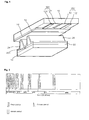
- FIG. 1 is a perspective view illustrating the construction of a discharge cell of a three-electrode AC surface discharge type PDP in a prior art.
- the discharge cell of the three-electrode AC surface discharge type PDP includes a scan electrode 30Y and a sustain electrode 30Z which are formed on the bottom surface of an upper substrate 10, and an address electrode 20X formed on a lower substrate 18.
- the scan electrode 30Y includes a transparent electrode 12Y, and a metal bus electrode 13Y which has a line width smaller than that of the transparent electrode 12Y and is disposed at one edge side of the transparent electrode.
- the sustain electrode 30Z includes a transparent electrode 12Z, and a metal bus electrode 13Z which has a line width smaller than that of the transparent electrode 12Z and is disposed at one side edge of the transparent electrode.
- the transparent electrodes 12Y, 12Z which are typically made of ITO (indium tin oxide), are formed on the bottom surface of the upper substrate 10.
- the metal bus electrodes 13Y, 13Z which are typically made of chrome (Cr), are formed on the transparent electrodes 12Y, 12Z, and serve to reduce a voltage drop caused by the transparent electrodes 12Y, 12Z having high resistance.
- On the bottom surface of the upper substrate 10 in which the scan electrodes 30Y and the sustain electrodes 30Z are placed in parallel with each other are laminated an upper dielectric layer 14 and a protective layer 16.
- the protective layer 16 serves to prevent the upper dielectric layer 14 from being damaged due to sputtering generated during the plasma discharge, and improve efficiency of secondary electron emission.
- Magnesium oxide (MgO) is typically used as the protective layer 16.
- a lower dielectric layer 22 and barrier ribs 24 are formed on the lower substrate 18 in which the address electrode 20X is formed.
- a phosphor layer 26 is coated on the surface of the lower dielectric layer 22 and barrier ribs 24.
- the address electrodes 20X are formed in the direction in which they intersect the scan electrodes 30Y and the sustain electrodes 30Z.
- the barrier ribs 24 are formed in parallel with the address electrodes 20X to prevent ultraviolet and a visible ray generated by the discharge from leaking toward neighboring discharge cells.
- the phosphor layer 26 is excited with an ultraviolet generated during the plasma discharging to generate a visible light of any one of red, green and blue lights.
- An inert mixed gas is injected into the discharge spaces defined between the upper substrate 10 and the barrier ribs 24 and between the lower substrate 18 and the barrier ribs 24.
- the PDP is time-driven with one frame being divided into several sub-fields having a different number of emission in order to implement the gray scale of an image.
- Each of the sub-fields is divided into a reset period for initializing the entire screen, an address period for selecting a scan line and selecting a cell from the selected scan line, and a sustain period for implementing the gray scale depending on the number of a discharge.
- the reset period is divided into a set-up period where a ramp-up pulse is supplied and a set-down period were a ramp-down pulse is supplied, in plural.
- a frame period (16.67ms) corresponding to 1/60 seconds is divided into eight sub-fields SF1 to SF8, as shown in FIG. 2.
- each of the eight sub-fields SF1 to SF8 is subdivided into a reset period, an address period and a sustain period.
- FIG. 3 shows a driving waveform of a PDP, which is supplied two sub-fields.
- Y indicates scan electrodes
- Z indicates sustain electrodes
- X indicates address electrodes
- the PDP is driven with it being divided into a reset period for initializing the entire screen, an address period for selecting a cell, and a sustain period for maintaining a discharge of the selected cell.
- a ramp-up pulse Ramp-up is applied to all scan electrodes Y at the same time.
- a weak discharge is generated within cells of the entire screen by means of the ramp-up pulse Ramp-up and wall charges are thus created within the cells.
- a ramp-down pulse Ramp-down which drops from a voltage of the positive polarity lower than the peak voltage of the ramp-up pulse Ramp-up, is applied to the scan electrodes Y at the same time.
- the ramp-down pulse Ramp-down generates a weak erase discharge within the cells, so that the wall charges generated by the set-up discharge and unnecessary charges among space charges are erased and wall charges necessary for an address discharge uniformly remain within the cells of the entire screen.
- a data pulse data of the positive polarity is applied to the address electrodes X.
- the address discharge is generated within cells to which the data pulse data is applied. Also, wall charges are generated within cells selected by the address discharge.
- a positive-polarity DC voltage of a sustain voltage level (Vs) is applied to the sustain electrodes Z.
- a sustain pulse sus is alternately applied to the scan electrodes Y and the sustain electrodes Z. Then, in cells selected by the address discharge, a sustain discharge is generated between the scan electrodes Y and the sustain electrodes Z in the surface discharge shape whenever the sustain pulse sus is applied as the wall voltage within the cells and the sustain pulse sus are added. Lastly, after the sustain discharge is completed, an erase ramp pulse erase having a narrow pulse width is applied to the sustain electrodes Z, thus erasing the wall charges within the cells.
- a discharge space is widened by increasing the height h of a barrier rib 24 so as to improve the emission efficiency of the PDP, as shown in FIG. 4. If the height of the barrier rib 24 is increased, however, a discharge firing voltage of an opposite discharge is increased. It is thus necessary to further lower the voltage of the ramp-down pulse Ramp-down. In this case, an excessive discharge is generated between the scan electrodes Y and the sustain electrodes Z. An erroneous discharge is thus generated in the address period or the sustain period.
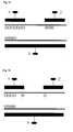
- the ramp-up pulse Ramp-up is applied to the scan electrodes Y in the set-up period, a discharge is generated between the scan electrodes Y and the sustain electrodes Z. Wall charges of the negative polarity are thus formed in the scan electrodes Y, as shown in FIG. 5a. It in turn means that a voltage of the negative polarity is applied to the sustain electrodes Z and the address electrodes X compared with the scan electrodes Y. Wall charges of the positive polarity are thus formed in the sustain electrodes Z and the address electrodes X.
- the ramp-down pulse Ramp-down be lower than the discharge firing voltage for generating the discharge between the scan electrodes Y and the address electrodes X. Accordingly, an excessive discharge is generated between the scan electrodes Y and the sustain electrodes Z, the wall charges in the scan electrodes Y and the sustain electrodes Z are excessively erased, as shown in FIG. 5c. Therefore, there is a problem in that the margin of the address discharge and the sustain discharge is lowered since the wall charges are severely inversed.
- the present invention has been made in view of the above problems, and it is an object of the present invention to provide a method of driving a plasma display panel in which a discharge can be generated stably.
- a method of driving a plasma display panel includes the step of alternately applying a first sustain pulse to scan electrode lines and sustain electrode lines during a sustain period with a first period intervened between the sustain periods. In this time, a last sustain pulse applied to the scan electrode lines during the sustain period is applied after a second period that is longer than the first period.
- a method of driving a plasma display panel in which one frame includes a plurality of selective write sub-fields and selective erase sub-fields includes the steps of alternately applying a first sustain pulse to scan electrode lines and sustain electrode lines during a sustain period of at least one of the plurality of the selective write sub-fields with a first period intervened between the sustain periods, and applying a last sustain pulse applied to the scan electrode lines after a second period that is longer than the first period.
- a method of driving a plasma display panel includes applying a last sustain pulse having a long pulse width, which is supplied to scan electrode lines in a last selective write sub-field, after sustain pulses that are provided previously. Accordingly, more particularly, in a low temperature environment, a stabilized sustain discharge can be generated by the last sustain pulse having the long pulse width. Thus, a stabilized address discharge can be generated in the address period of the selective erase sub-field.
- a method of driving a plasma display panel including the steps of applying a first ramp-down pulse having a first tilt to scan electrodes in the first half of a set-down period included in a reset period, applying a ground voltage to the scan electrodes in the meddle phase of the set-down period, and applying a second ramp-down pulse having a second tilt to the scan electrodes in the second half of the set-down period.
- a method of driving a plasma display panel in which a reset period is divided into a set-up period and a set-down period and is then driven, including a first step in which wall charges are formed in a discharge cell during the set-up period, a second step in which some of the wall charges is erased by a discharge between scan electrodes and sustain electrodes during the first half of the set-down period, and a third step in which some of the wall charges is erased by a discharge between the scan electrodes and address electrodes in the second half of the set-down period.
- an apparatus for driving a plasma display panel including a scan driving unit that supplies a first ramp-down pulse which drops from a sustain voltage to a ground voltage at a first tilt in the first half of a set-down period included in the reset period, supplies the ground voltage in the meddle phase of the set-down period, and supplies a second ramp-down pulse which drops from the ground voltage to a voltage of the negative polarity at a second tilt in the second half of the set-down period; and a sustain driving unit that supplies the sustain voltage in the first half of the set-down period and the ground voltage in the second half of the set-down period.
- the present invention has an effect in that it can generate a reset discharge and an address discharge stably.
- the present invention has been made in view of the above problems, and it is an object of the present invention to provide a method of driving a plasma display panel in which a discharge can be generated stably.
- a method of driving a plasma display panel includes the step of alternately applying a first sustain pulse to scan electrode lines and sustain electrode lines during a sustain period with a first period intervened between the sustain periods. In this time, a last sustain pulse applied to the scan electrode lines during the sustain period is applied after a second period that is longer than the first period.
- a method of driving a plasma display panel in which one frame includes a plurality of selective write sub-fields and selective erase sub-fields includes the steps of alternately applying a first sustain pulse to scan electrode lines and sustain electrode lines during a sustain period of at least one of the plurality of the selective write sub-fields with a first period intervened between the sustain periods, and applying a last sustain pulse applied to the scan electrode lines after a second period that is longer than the first period.
- a method of driving a plasma display panel includes applying a last sustain pulse having a long pulse width, which is supplied to scan electrode lines in a last selective write sub-field, after sustain pulses that are provided previously. Accordingly, more particularly, in a low temperature environment, a stabilized sustain discharge can be generated by the last sustain pulse having the long pulse width. Thus, a stabilized address discharge can be generated in the address period of the selective erase sub-field.
- a method of driving a plasma display panel including the steps of applying a first ramp-down pulse having a first tilt to scan electrodes in the first half of a set-down period included in a reset period, applying a ground voltage to the scan electrodes in the meddle phase of the set-down period, and applying a second ramp-down pulse having a second tilt to the scan electrodes in the second half of the set-down period.
- the first ramp-down pulse preferably drops from a sustain voltage level to the ground voltage.
- the second ramp-down pulse preferably drops from the ground voltage to a voltage level of the negative polarity.
- the voltage level of the negative polarity is preferably a voltage of -100V or less.
- the first tilt and the second tilt may be set to be the same.
- the first tilt and the second tilt may be set to be different.
- the first tilt may be set to be higher than the second tilt.
- the first tilt may be set to be lower than the second tilt.
- a first voltage of the positive polarity may be supplied to the sustain electrodes.
- the ground voltage may be supplied to the sustain electrodes.
- a second voltage of the positive polarity which is lower than the first voltage of the positive polarity, may be supplied to the sustain electrodes during an address period.
- a method of driving a plasma display panel in which a reset period is divided into a set-up period and a set-down period and is then driven, including a first step in which wall charges are formed in a discharge cell during the set-up period, a second step in which some of the wall charges is erased by a discharge between scan electrodes and sustain electrodes during the first half of the set-down period, and a third step in which some of the wall charges is erased by a discharge between the scan electrodes and address electrodes in the second half of the set-down period.
- the method of driving the plasma display panel according to an embodiment of the present invention preferably further includes the step of supplying a ground voltage to the scan electrodes between the second and third steps.
- an apparatus for driving a plasma display panel including a scan driving unit that supplies a first ramp-down pulse which drops from a sustain voltage to a ground voltage at a first tilt in the first half of a set-down period included in the reset period, supplies the ground voltage in the meddle phase of the set-down period, and supplies a second ramp-down pulse which drops from the ground voltage to a voltage of the negative polarity at a second tilt in the second half of the set-down period; and a sustain driving unit that supplies the sustain voltage in the first half of the set-down period and the ground voltage in the second half of the set-down period.
- the sustain driving unit preferably supplies a voltage of the positive polarity that is lower than the sustain voltage to sustain electrodes during the address period.
- the first tilt and the second tilt may be set to be the same.
- the first tilt and the second tilt may be set to be different.
- the first tilt may be set to be higher than the second tilt.
- the first tilt may be set to be lower than the second tilt.
- the scan driving unit may include a first ramp supply unit for supplying the first ramp-down pulse having the first tilt, and a second ramp supply unit for supplying the second ramp-down pulse having the second tilt.
- the first ramp supply unit may include a first switch connected between a sustain voltage source and a ground voltage source, and a first variable resistor connected to the gate terminal of the first switch, for controlling the first tilt of the first ramp-down pulse.
- the second ramp supply unit may include a second switch connected between a sustain voltage source and a negative-polarity voltage source, and a second variable resistor connected to the gate terminal of the second switch, for controlling the second tilt of the second ramp-down pulse.
- the negative-polarity voltage source preferably supplies a voltage of -100V or less.
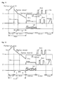
- FIG. 6 is a waveform for explaining a method of driving a PDP according to an embodiment of the present invention the plasma display panel.
- the PDP has a barrier rib the height of which is increased so as to improve the discharge efficiency.
- Y indicates scan electrodes
- Z indicates sustain electrodes
- X indicates address electrodes
- the PDP includes a reset period for initializing the entire screen, an address period for selecting a given cell, and a sustain period for maintaining a discharge of the selected cell.
- a ramp-up pulse Ramp-up is applied to all the scan electrodes Y at the same time.
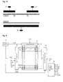
- a weak discharge is generated in cells of the entire screen by the ramp-up pulse Ramp-up, so that wall charges are formed in the cells as shown in FIG. 7a.
- the ramp-up pulse Ramp-up is raised up to a peak voltage (Vy), and the peak voltage (Vy) is then applied to the scan electrodes Y for a predetermined time. If the peak voltage (Vy) of the ramp-up pulse Ramp-up is maintained for a predetermined time, the wall charges formed in the discharge cell are enhanced.
- a first ramp-down pulse Ramp-down1 having a first tilt is applied to the scan electrodes Y.
- a second ramp-down pulse Ramp-down2 having a second tilt is applied to the scan electrodes Y.
- the first tilt is set to be lower than the second tilt.
- the first ramp-down pulse Ramp-down1 which is applied during the "a" period, drops to a ground voltage at a time point where the voltage drops from the peak voltage (Vy) to a sustain voltage (Vs).
- the sustain voltage (Vs) of a positive-polarity DC voltage is applied to the sustain electrodes Z. Accordingly, an erase discharge, i.e., a dark discharge is generated within the cells between the scan electrodes Y and the sustain electrodes Z, so the wall charges generated by the set-up discharge and unnecessary charges among space charges are erased. Therefore, the wall charges are formed, as shown in FIG. 7b. Meanwhile, if the second ramp-down pulse Ramp-donw2 is applied immediately after the first ramp-down pulse Ramp-donw1 is applied, an erroneous discharge can occur between the scan electrodes Y and the sustain electrodes Z. In order to prevent this erroneous discharge, the ground voltage is applied to the scan electrodes Y for a given time.
- the second ramp-down pulse Ramp-down2 having the second tilt which drops to a predetermined voltage of the negative polarity (e.g., -100V or less), is applied to the scan electrodes Y. That is, if the height of the barrier rib is increased so as to improve the discharge efficiency, a distance between the scan electrodes Y and the address electrodes X becomes far and the discharge firing voltage is thus increased. Accordingly, a dark discharge is generated between the scan electrodes Y and the address electrodes Z by dropping the second ramp-down pulse Ramp-down2 having the second tilt below the discharge firing voltage.
- a predetermined voltage of the negative polarity e.g., -100V or less
- the ground voltage is applied to the sustain electrodes Z. Accordingly, since a discharge is not generated between the scan electrodes Y and the sustain electrodes Z, the wall charges formed in the sustain electrodes Z are not affected.
- the first and second ramp-down pulses Ramp-down1, Ramp-down2, which have a different tilt, are applied to the scan electrodes Y.
- the dark discharge is generated between the scan electrodes Y and the sustain electrodes Z by the first ramp-down pulse Ramp-down1
- the dark discharge is generated between the scan electrodes Y and the address electrodes X by the second ramp-down pulse Ramp-donw2, so that wall charges are formed as shown in FIG. 7c.
- Distribution of the wall charges between the scan electrodes Y and the sustain electrodes Z and between the scan electrodes Y and the address electrodes X can be controlled individually by applying the first and second ramp-down pulses Ramp-down1, Ramp-down2 having a different tilt to the scan electrodes Y.
- the height of the barrier rib is increased so as to improve the discharge efficiency, it is prevented lots of wall charges of the positive polarity from being formed in the scan electrodes Y and lots wall charges of the negative polarity from being form in the sustain electrodes Z. Resultantly, an excessive erase is not generated between the scan electrode Y and the sustain electrodes Z, and a stabilized address discharge can be generated in the address period accordingly.
- a data pulse data of the positive polarity which has a data voltage (Vd) is applied to the address electrodes X.
- Vd data voltage
- an address discharge is generated within cells to which the data pulse data is applied. Wall charges are thus formed in cells selected by the address discharge.
- a DC voltage of the positive polarity which is lower than the sustain voltage level (Vs) is applied to the sustain electrodes Z so that the address discharge is generated between the scan electrode Y and the address electrodes X.
- a sustain pulse Sus is alternately applied to the scan electrodes Y and the sustain electrodes Z. Then, in cells selected by the address discharge, a sustain discharge is generated in a surface discharge shape between the scan electrode Y and the sustain electrodes Z whenever the sustain pulse Sus is applied as the wall voltage and the sustain pulse Sus within the cells are added. Finally, after the sustain discharge is completed, an erase ramp pulse erase having a small pulse width is applied to the sustain electrodes Z, thus erasing the wall charges within the cells.
- FIG. 8 is a block diagram illustrating the construction of an apparatus for driving the PDP for generating the waveform shown in FIG. 6.
- the apparatus includes a data driving unit 72 for supplying data to address electrodes X1 to Xm, a scan driving unit 73 for driving scan electrodes Y1 to Yn, a sustain driving unit 74 for driving a sustain electrode Z being a common electrode, a timing controller 71 for controlling the respective driving units 72, 73 and 74, and a driving voltage generator 75 for supplying driving voltages which are necessary for the respective driving units 72, 73 and 74 thereto.
- a data driving unit 72 for supplying data to address electrodes X1 to Xm
- a scan driving unit 73 for driving scan electrodes Y1 to Yn
- a sustain driving unit 74 for driving a sustain electrode Z being a common electrode
- a timing controller 71 for controlling the respective driving units 72, 73 and 74
- a driving voltage generator 75 for supplying driving voltages which are necessary for the respective driving units 72, 73 and 74 thereto.
- the data driving unit 72 is supplied with data which undergo inverse-gamma correction and error diffusion operations by an inverse-gamma correction circuit and an error diffusion circuit (not shown and are then mapped to respective sub-fields by a sub-field mapping circuit.
- the data driving unit 72 serves to sample and latch the data in response to a timing control signal CTRX from the timing controller 71 and to supply the data to the address electrodes X1 to Xm.
- the scan driving unit 73 supplies the ramp-up pulse Ramp-up to the scan electrodes Y1 to Yn during the set-up period of the reset period, the first ramp-down pulse Ramp-down1 having the first tilt to the scan electrodes Y1 to Yn during the "a" period of the set-down period, and the second ramp-down pulse Ramp-down2 having the second tilt to the scan electrodes Y1 to Yn during the "b" period, under the control of the timing controller 71.
- the first tilt is set to be lower than the second tilt.
- the scan driving unit 73 sequentially applies the scan pulse to the scan electrodes Y1 to Yn during the address period, and then applies the sustain pulse Sus to the scan electrodes Y1 to Yn during the sustain period, under the control of the timing controller 71.
- the sustain driving unit 74 provides the ground voltage or 0V to the sustain electrodes Z during the set-up period of the reset period, the positive-polarity DC voltage of the sustain voltage level (Vs) to the sustain electrodes Z during the "a" period of the set-down period, and then the ground voltage or 0V to the sustain electrodes Z during the "b" period of the set-down period, under the control of the timing controller 71. Furthermore, the sustain driving unit 74 constantly supplies a DC voltage (Vzdc), which is lower than the sustain voltage (Vs), to the sustain electrodes Z1 to Zn during the address period under the control the timing controller 71, and then supplies the sustain pulse Sus to the sustain electrodes Z during the sustain period, while operating alternately with the scan driving unit 73.
- Vzdc DC voltage
- the timing controller 71 receives vertical/horizontal synchronization signals, generates timing control signals CTRX, CTRY and CTRZ which are necessary for the driving units, respectively, and supplies the timing control signals CTRX, CTRY and CTRZ to corresponding driving units 72, 73 and 74, thereby controlling the driving units 72, 73 and 74.
- the data control signal CTRX includes a sampling clock for sampling a data, a latch control signal, and a switch control signal for controlling an on/off time of an energy recovery circuit and a driving switch element.
- the scan control signal CTRY includes a switch control signal for controlling an on/off time of an energy recovery circuit and a driving switch element within the scan driving unit 73.
- the sustain control signal CTRZ includes a switch control signal for controlling an on/off time of an energy recovery circuit and a driving switch element within the sustain driving unit 74.
- the driving voltage generator 75 serves to generate the voltage (Vry) of the ramp-up pulse Ramp-up, the voltage (-Vny) of the second ramp-down pulse Ramp-down2, the DC voltage (Vzdc) supplied to the sustain electrodes Z during the address period, a scan bias voltage (Vscb), a scan voltage (-Vscan), the sustain voltage (Vs), the data voltage (Vd) and the like. It is to be noted that these driving voltages may vary depending on the composition of a discharge gas or the construction of a discharge cell.
- FIG. 9 is a detailed circuit diagram showing some of the scan driving unit 73 and the sustain driving unit 74 for driving the pair of the scan electrodes Y and the sustain electrodes Z.
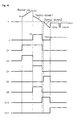
- FIG. 10 is a waveform showing the operational timing of switch elements included in the scan driving unit 73 and the sustain driving unit 74.
- the scan driving unit 73 includes an energy recovery circuit 81, a driving switch circuit 82, and first to sixth switch elements Q1 to Q6.
- the energy recovery circuit 81 recovers energy of invalid power, which does not contribute to a discharge in a PDP, from the scan electrodes Y, and charges the scan electrodes Y with the recovered energy.
- the energy recovery circuit 81 can be implemented using any known energy recovery circuit.
- the driving switch circuit 82 includes a scan bias voltage source (Vscb), and seventh and eighth switch elements Q7, Q8 which are connected between first nodes n1 in a push-pull shape.
- the output terminal between the seventh and eighth switch elements Q7, Q8 is connected to the scan electrodes Y.
- Each of the seventh and eighth switch elements Q7, Q8 supplies the scan bias voltage (Vscb) or the voltage on the first node n1 to the scan electrodes, Y under the control of the timing controller 71.
- the first switch element Q1 is connected between a sustain voltage source (Vs) and the first node n1, and provides the sustain voltage (Vs) to the first node n1 under the control of the timing controller 71.
- the second switch element Q2 is connected between a ground voltage source (GND) and the first node n1, and supplies the ground voltage (GND) to the first node n1 under the control of the timing controller 71.
- GND ground voltage source
- the third switch element Q3 is connected between a ramp-up voltage source (Vry) and the first node n1.
- the third switch element Q3 applies a ramp-up pulse Ramp-up to the first node n1 at a tilt, which is determined according to a preset RC time constant, under the control of the timing controller 71.
- To the control terminal of the third switch element Q3 is connected a variable resistor VR1 and a capacitor (not shown), for controlling the tilt of the ramp-up pulse Ramp-up.
- the fourth switch element Q4 is connected between the ground voltage source (GND) and the first node n1.
- the fourth switch element Q4 applies a first ramp-down pulse Ramp-down1 to the first node n1 at a tilt, which is determined according to a preset RC time constant, under the control of the timing controller 71.
- To the control terminal of the fourth switch element Q4 is connected a variable resistor VR2 and a capacitor (not shown), for controlling the tilt of the first ramp-down pulse Ramp-down1.
- the fifth switch element Q5 is connected between a ramp-down voltage source (-Vy) and the first node n1.
- the fifth switch element Q5 supplies a second ramp-down pulse Ramp-down2 to the first node n1 at a tilt, which is determined according to a preset RC time constant, under the control of the timing controller 71.
- To the control terminal of the fifth switch element Q5 is connected a variable resistor VR3 and a capacitor (not shown), for controlling the tilt of the second ramp-down pulse Ramp-down2.
- the sixth switch element Q6 is connected between the scan voltage source and the first node n1, and supplies the scan voltage (-Vscan) to the first node n1 under the control of the timing controller 71.
- the sustain driving unit 74 includes an energy recovery circuit 83, and ninth to eleventh switch elements Q9 to Q11.
- the energy recovery circuit 83 recovers energy of invalid power which does not contribute to a discharge in the PDP from the sustain electrodes Z, and charges the sustain electrodes Z with the recovered energy.
- the energy recovery circuit 83 can be implemented using any known energy recovery circuit.
- the ninth switch element Q9 is connected between the sustain voltage source (Vs) and the second node n2, and supplies a sustain voltage (Vs) to the second node n2, i.e., the sustain electrodes Z, under the control of the timing controller 71.
- the tenth switch element Q10 is connected between the ground voltage source (GND) and the second node n2, and supplies the ground voltage (GND) to the second node n2 under the control of the timing controller 71.
- the eleventh switch element Q11 is connected between a DC voltage source (Vzdc) the voltage of which is lower than the sustain voltage (Vs) and the second node n2, and supplies the DC voltage (Vzdc) to the second node n2 during the address period under the control of the timing controller 71.
- Vzdc DC voltage source
- the tilt of the first ramp-down pulse Ramp-down1 which is supplied during the "a" period of the set-down period of the reset period can be set to be higher than that of the second ramp-down pulse Ramp-down2 which is supplied in the "b" period.
- the tilt of the first ramp-down pulse Ramp-down1 that is supplied in the "a" period of the set-down period of the reset period can be set to be the same as that of the second ramp-down pulse Ramp-down2 that is supplied in the "b" period.
- the tilts of the first and second ramp-down pulses Ramp-down1, Ramp-down2 that are supplied in the set-down period is set to be the same or different, it is possible to effectively cope with conditions of various panels. That is, during the "a" period of the set-down period, the first ramp-down pulse Ramp-down1 is supplied to control wall charges between the scan electrodes Y and the sustain electrodes Z. During the "b" period of the set-down period, the second ramp-down pulse Ramp-down2 a tilt of which is the same as or different from that of the first ramp-down pulse Ramp-down1 is supplied to control wall charges between the scan electrodes Y and the address electrodes X. It is thus possible to effectively meet conditions of various panels.
- first and second ramp-down pulses having the same tilt or a different tilt are applied during a set-down period of a reset period.
- distribution of wall charges between scan electrodes and sustain electrodes and between the scan electrodes and address electrodes is individually controlled. This has an effect in that it can generate a reset discharge and an address discharge stably.
Landscapes
- Engineering & Computer Science (AREA)
- Physics & Mathematics (AREA)
- Power Engineering (AREA)
- Plasma & Fusion (AREA)
- Computer Hardware Design (AREA)
- General Physics & Mathematics (AREA)
- Theoretical Computer Science (AREA)
- Control Of Indicators Other Than Cathode Ray Tubes (AREA)
- Control Of Gas Discharge Display Tubes (AREA)
- Transforming Electric Information Into Light Information (AREA)
Abstract
Description
- The present invention relates to a method of driving a plasma display panel and apparatus thereof, and more particularly, to a method of driving a plasma display panel in which the margin of an address discharge and a sustain discharge are increased through a stabilized reset operation, and apparatus thereof.
- Plasma display panels (hereinafter, referred to as a 'PDPs') are adapted to display images by light-emitting phosphors stimulated with ultraviolet light generated during the discharge of an inert mixed gas such as He+Xe, Ne+Xe or He+Ne+Xe. Such PDPs can be easily made both thin and large, and can provide greatly increased image quality with recent developments of the relevant technology.
- FIG. 1 is a perspective view illustrating the construction of a discharge cell of a three-electrode AC surface discharge type PDP in a prior art.
- Referring to FIG. 1, the discharge cell of the three-electrode AC surface discharge type PDP includes a
scan electrode 30Y and a sustain electrode 30Z which are formed on the bottom surface of anupper substrate 10, and anaddress electrode 20X formed on alower substrate 18. Thescan electrode 30Y includes atransparent electrode 12Y, and ametal bus electrode 13Y which has a line width smaller than that of thetransparent electrode 12Y and is disposed at one edge side of the transparent electrode. The sustain electrode 30Z includes atransparent electrode 12Z, and ametal bus electrode 13Z which has a line width smaller than that of thetransparent electrode 12Z and is disposed at one side edge of the transparent electrode. - The
transparent electrodes upper substrate 10. Themetal bus electrodes transparent electrodes transparent electrodes upper substrate 10 in which thescan electrodes 30Y and the sustain electrodes 30Z are placed in parallel with each other are laminated an upperdielectric layer 14 and aprotective layer 16. On the upperdielectric layer 14 are accumulated wall charges generated during plasma discharge. Theprotective layer 16 serves to prevent the upperdielectric layer 14 from being damaged due to sputtering generated during the plasma discharge, and improve efficiency of secondary electron emission. Magnesium oxide (MgO) is typically used as theprotective layer 16. - A lower
dielectric layer 22 andbarrier ribs 24 are formed on thelower substrate 18 in which theaddress electrode 20X is formed. Aphosphor layer 26 is coated on the surface of the lowerdielectric layer 22 andbarrier ribs 24. Theaddress electrodes 20X are formed in the direction in which they intersect thescan electrodes 30Y and the sustain electrodes 30Z. Thebarrier ribs 24 are formed in parallel with theaddress electrodes 20X to prevent ultraviolet and a visible ray generated by the discharge from leaking toward neighboring discharge cells. Thephosphor layer 26 is excited with an ultraviolet generated during the plasma discharging to generate a visible light of any one of red, green and blue lights. An inert mixed gas is injected into the discharge spaces defined between theupper substrate 10 and thebarrier ribs 24 and between thelower substrate 18 and thebarrier ribs 24. - The PDP is time-driven with one frame being divided into several sub-fields having a different number of emission in order to implement the gray scale of an image. Each of the sub-fields is divided into a reset period for initializing the entire screen, an address period for selecting a scan line and selecting a cell from the selected scan line, and a sustain period for implementing the gray scale depending on the number of a discharge.
- In this time, the reset period is divided into a set-up period where a ramp-up pulse is supplied and a set-down period were a ramp-down pulse is supplied, in plural. For example, if it is desired to display an image with 256 gray scale, a frame period (16.67ms) corresponding to 1/60 seconds is divided into eight sub-fields SF1 to SF8, as shown in FIG. 2. Furthermore, each of the eight sub-fields SF1 to SF8 is subdivided into a reset period, an address period and a sustain period. In this time, the reset period and the address period of each of the sub-fields are the same every sub-field, whereas the sustain period and the number of a sustain pulse allocated thereto are increased in the ratio of 2n(n=0,1,2,3,4,5,6,7) in each sub-field.
- FIG. 3 shows a driving waveform of a PDP, which is supplied two sub-fields.
- In FIG. 3, Y indicates scan electrodes, Z indicates sustain electrodes and X indicates address electrodes.
- Referring to FIG. 3, the PDP is driven with it being divided into a reset period for initializing the entire screen, an address period for selecting a cell, and a sustain period for maintaining a discharge of the selected cell.
- In a set-up period of the reset period, a ramp-up pulse Ramp-up is applied to all scan electrodes Y at the same time. A weak discharge is generated within cells of the entire screen by means of the ramp-up pulse Ramp-up and wall charges are thus created within the cells. In a set-down period, a ramp-down pulse Ramp-down, which drops from a voltage of the positive polarity lower than the peak voltage of the ramp-up pulse Ramp-up, is applied to the scan electrodes Y at the same time. The ramp-down pulse Ramp-down generates a weak erase discharge within the cells, so that the wall charges generated by the set-up discharge and unnecessary charges among space charges are erased and wall charges necessary for an address discharge uniformly remain within the cells of the entire screen.
- In the address period, simultaneously when a scan pulse scan of the negative polarity is sequentially applied to the scan electrodes Y, a data pulse data of the positive polarity is applied to the address electrodes X. As a voltage difference between the scan pulse scan and the data pulse data and a wall voltage generated in the reset period are added, the address discharge is generated within cells to which the data pulse data is applied. Also, wall charges are generated within cells selected by the address discharge.
- Meanwhile, during the set-down period and the address period, a positive-polarity DC voltage of a sustain voltage level (Vs) is applied to the sustain electrodes Z.
- In the sustain period, a sustain pulse sus is alternately applied to the scan electrodes Y and the sustain electrodes Z. Then, in cells selected by the address discharge, a sustain discharge is generated between the scan electrodes Y and the sustain electrodes Z in the surface discharge shape whenever the sustain pulse sus is applied as the wall voltage within the cells and the sustain pulse sus are added. Lastly, after the sustain discharge is completed, an erase ramp pulse erase having a narrow pulse width is applied to the sustain electrodes Z, thus erasing the wall charges within the cells.
- Meanwhile, there has been proposed a structure in which a discharge space is widened by increasing the height h of a
barrier rib 24 so as to improve the emission efficiency of the PDP, as shown in FIG. 4. If the height of thebarrier rib 24 is increased, however, a discharge firing voltage of an opposite discharge is increased. It is thus necessary to further lower the voltage of the ramp-down pulse Ramp-down. In this case, an excessive discharge is generated between the scan electrodes Y and the sustain electrodes Z. An erroneous discharge is thus generated in the address period or the sustain period. - This will be below described in detail. If the ramp-up pulse Ramp-up is applied to the scan electrodes Y in the set-up period, a discharge is generated between the scan electrodes Y and the sustain electrodes Z. Wall charges of the negative polarity are thus formed in the scan electrodes Y, as shown in FIG. 5a. It in turn means that a voltage of the negative polarity is applied to the sustain electrodes Z and the address electrodes X compared with the scan electrodes Y. Wall charges of the positive polarity are thus formed in the sustain electrodes Z and the address electrodes X. Thereafter, if the ramp-down pulse Ramp-down is applied to the scan electrodes Y and the DC voltage of the positive polarity is applied to the sustain electrodes Z in a set-down period, a weak discharge is generated between the scan electrodes Y and the sustain electrodes Z, thus erasing the wall charges. Accordingly, wall charges are formed, as shown in FIG. 5b. If the height of the barrier rib is increased so as to improve the discharge efficiency, however, the distance between the scan electrodes Y and the address electrodes Z becomes greater. Therefore, in order to generate a discharge between the scan electrodes Y and the address electrodes X, it is required that the ramp-down pulse Ramp-down be lower than the discharge firing voltage for generating the discharge between the scan electrodes Y and the address electrodes X. Accordingly, an excessive discharge is generated between the scan electrodes Y and the sustain electrodes Z, the wall charges in the scan electrodes Y and the sustain electrodes Z are excessively erased, as shown in FIG. 5c. Therefore, there is a problem in that the margin of the address discharge and the sustain discharge is lowered since the wall charges are severely inversed.
- Accordingly, the present invention has been made in view of the above problems, and it is an object of the present invention to provide a method of driving a plasma display panel in which a discharge can be generated stably.
- According to an aspect of the present invention, a method of driving a plasma display panel includes the step of alternately applying a first sustain pulse to scan electrode lines and sustain electrode lines during a sustain period with a first period intervened between the sustain periods. In this time, a last sustain pulse applied to the scan electrode lines during the sustain period is applied after a second period that is longer than the first period.
- According to another aspect of the present invention, a method of driving a plasma display panel in which one frame includes a plurality of selective write sub-fields and selective erase sub-fields includes the steps of alternately applying a first sustain pulse to scan electrode lines and sustain electrode lines during a sustain period of at least one of the plurality of the selective write sub-fields with a first period intervened between the sustain periods, and applying a last sustain pulse applied to the scan electrode lines after a second period that is longer than the first period.
- According to still another aspect of the present invention, a method of driving a plasma display panel includes applying a last sustain pulse having a long pulse width, which is supplied to scan electrode lines in a last selective write sub-field, after sustain pulses that are provided previously. Accordingly, more particularly, in a low temperature environment, a stabilized sustain discharge can be generated by the last sustain pulse having the long pulse width. Thus, a stabilized address discharge can be generated in the address period of the selective erase sub-field.
- According to another aspect of the present invention, there is provided a method of driving a plasma display panel, including the steps of applying a first ramp-down pulse having a first tilt to scan electrodes in the first half of a set-down period included in a reset period, applying a ground voltage to the scan electrodes in the meddle phase of the set-down period, and applying a second ramp-down pulse having a second tilt to the scan electrodes in the second half of the set-down period.
- According to another aspect of the present invention, there is provided a method of driving a plasma display panel in which a reset period is divided into a set-up period and a set-down period and is then driven, including a first step in which wall charges are formed in a discharge cell during the set-up period, a second step in which some of the wall charges is erased by a discharge between scan electrodes and sustain electrodes during the first half of the set-down period, and a third step in which some of the wall charges is erased by a discharge between the scan electrodes and address electrodes in the second half of the set-down period.
- According to another aspect of the present invention, there is provided an apparatus for driving a plasma display panel, including a scan driving unit that supplies a first ramp-down pulse which drops from a sustain voltage to a ground voltage at a first tilt in the first half of a set-down period included in the reset period, supplies the ground voltage in the meddle phase of the set-down period, and supplies a second ramp-down pulse which drops from the ground voltage to a voltage of the negative polarity at a second tilt in the second half of the set-down period; and a sustain driving unit that supplies the sustain voltage in the first half of the set-down period and the ground voltage in the second half of the set-down period.
- The present invention has an effect in that it can generate a reset discharge and an address discharge stably.
- Embodiments of the invention will be described in detail with reference to the following drawings in which like numerals refer to like elements.
- FIG. 1 is a perspective view illustrating the construction of a three-electrode AC surface discharge type PDP in a prior art;
- FIG. 2 shows one frame of the AC surface discharge type PDP in the prior art;
- FIG. 3 shows a driving waveform which is provided to the electrodes during the sub-field shown in FIG. 2;
- FIG. 4 is a cross-sectional view showing a plasma display panel having a barrier rib of a height h;
- FIG. 5a shows wall charges formed in the set-up period of the reset period in the driving waveform shown in FIG. 3;
- FIG. 5b shows wall charges that must be formed in the set-down period of the reset period in the driving waveform shown in FIG. 3;
- FIG. 5c shows wall charges formed in the set-down period of the reset period when the driving waveform shown in FIG. 3 is supplied to the PDP shown in FIG. 4;
- FIG. 6 shows a driving waveform for explaining a method of driving a PDP according to an embodiment of the present invention;
- FIG. 7a shows wall charges formed in the set-up period of the reset period in the driving waveform shown in FIG. 6;
- FIG. 7b shows wall charges formed by a first ramp-down pulse during the set-down period of the reset period in the driving waveform shown in FIG. 6;
- FIG. 7c shows wall charges formed by a second ramp-down pulse during the set-down period of the reset period in the driving waveform shown in FIG. 6;
- FIG. 8 is a block diagram illustrating the construction of an apparatus for driving the PDP for generating the driving waveform shown in FIG. 6;
- FIG. 9 is a detailed circuit diagram of the scan driving unit and the sustain driving unit shown in FIG. 8;
- FIG. 10 shows a waveform for explaining the operation of the switch element shown in FIG. 9; and
- FIGS. 11 and 12 show waveforms for explaining a method of driving a PDP, which is different from that shown in FIG. 6.
-
- Preferred embodiments of the present invention will be described in a more detailed manner with reference to the drawings.
- Accordingly, the present invention has been made in view of the above problems, and it is an object of the present invention to provide a method of driving a plasma display panel in which a discharge can be generated stably.
- According to an embodiment of the present invention, a method of driving a plasma display panel includes the step of alternately applying a first sustain pulse to scan electrode lines and sustain electrode lines during a sustain period with a first period intervened between the sustain periods. In this time, a last sustain pulse applied to the scan electrode lines during the sustain period is applied after a second period that is longer than the first period.
- According to another embodiment of the present invention, a method of driving a plasma display panel in which one frame includes a plurality of selective write sub-fields and selective erase sub-fields includes the steps of alternately applying a first sustain pulse to scan electrode lines and sustain electrode lines during a sustain period of at least one of the plurality of the selective write sub-fields with a first period intervened between the sustain periods, and applying a last sustain pulse applied to the scan electrode lines after a second period that is longer than the first period.
- According to still embodiment of the present invention, a method of driving a plasma display panel includes applying a last sustain pulse having a long pulse width, which is supplied to scan electrode lines in a last selective write sub-field, after sustain pulses that are provided previously. Accordingly, more particularly, in a low temperature environment, a stabilized sustain discharge can be generated by the last sustain pulse having the long pulse width. Thus, a stabilized address discharge can be generated in the address period of the selective erase sub-field.
- According to an embodiment of the present invention, there is provided a method of driving a plasma display panel, including the steps of applying a first ramp-down pulse having a first tilt to scan electrodes in the first half of a set-down period included in a reset period, applying a ground voltage to the scan electrodes in the meddle phase of the set-down period, and applying a second ramp-down pulse having a second tilt to the scan electrodes in the second half of the set-down period.
- In the method of driving the plasma display panel according to an embodiment of the present invention, the first ramp-down pulse preferably drops from a sustain voltage level to the ground voltage.
- In the method of driving the plasma display panel according to an embodiment of the present invention, the second ramp-down pulse preferably drops from the ground voltage to a voltage level of the negative polarity.
- In the method of driving the plasma display panel according to an embodiment of the present invention, the voltage level of the negative polarity is preferably a voltage of -100V or less.
- In the method of driving the plasma display panel according to an embodiment of the present invention, the first tilt and the second tilt may be set to be the same.
- In the method of driving the plasma display panel according to an embodiment of the present invention, the first tilt and the second tilt may be set to be different.
- In the method of driving the plasma display panel according to an embodiment of the present invention, the first tilt may be set to be higher than the second tilt.
- In the method of driving the plasma display panel according to an embodiment of the present invention, the first tilt may be set to be lower than the second tilt.
- In the method of driving the plasma display panel according to an embodiment of the present invention, in the first half of the set-down period, a first voltage of the positive polarity may be supplied to the sustain electrodes.
- In the method of driving the plasma display panel according to an embodiment of the present invention, in the second half of the set-down period, the ground voltage may be supplied to the sustain electrodes.
- In the method of driving the plasma display panel according to an embodiment of the present invention, a second voltage of the positive polarity, which is lower than the first voltage of the positive polarity, may be supplied to the sustain electrodes during an address period.
- According to an embodiment of the present invention, there is provided a method of driving a plasma display panel in which a reset period is divided into a set-up period and a set-down period and is then driven, including a first step in which wall charges are formed in a discharge cell during the set-up period, a second step in which some of the wall charges is erased by a discharge between scan electrodes and sustain electrodes during the first half of the set-down period, and a third step in which some of the wall charges is erased by a discharge between the scan electrodes and address electrodes in the second half of the set-down period.
- The method of driving the plasma display panel according to an embodiment of the present invention preferably further includes the step of supplying a ground voltage to the scan electrodes between the second and third steps.
- According to an embodiment of the present invention, there is provided an apparatus for driving a plasma display panel, including a scan driving unit that supplies a first ramp-down pulse which drops from a sustain voltage to a ground voltage at a first tilt in the first half of a set-down period included in the reset period, supplies the ground voltage in the meddle phase of the set-down period, and supplies a second ramp-down pulse which drops from the ground voltage to a voltage of the negative polarity at a second tilt in the second half of the set-down period; and a sustain driving unit that supplies the sustain voltage in the first half of the set-down period and the ground voltage in the second half of the set-down period.
- In the apparatus of driving the plasma display panel according to an embodiment of the present invention, the sustain driving unit preferably supplies a voltage of the positive polarity that is lower than the sustain voltage to sustain electrodes during the address period.
- In the apparatus of driving the plasma display panel according to an embodiment of the present invention, the first tilt and the second tilt may be set to be the same.
- In the apparatus of driving the plasma display panel according to an embodiment of the present invention, the first tilt and the second tilt may be set to be different.
- In the apparatus of driving the plasma display panel according to an embodiment of the present invention, the first tilt may be set to be higher than the second tilt.
- In the apparatus of driving the plasma display panel according to an embodiment of the present invention, the first tilt may be set to be lower than the second tilt.
- In the apparatus of driving the plasma display panel according to an embodiment of the present invention, the scan driving unit may include a first ramp supply unit for supplying the first ramp-down pulse having the first tilt, and a second ramp supply unit for supplying the second ramp-down pulse having the second tilt.
- In the apparatus of driving the plasma display panel according to an embodiment of the present invention, the first ramp supply unit may include a first switch connected between a sustain voltage source and a ground voltage source, and a first variable resistor connected to the gate terminal of the first switch, for controlling the first tilt of the first ramp-down pulse.
- In the apparatus of driving the plasma display panel according to an embodiment of the present invention, the second ramp supply unit may include a second switch connected between a sustain voltage source and a negative-polarity voltage source, and a second variable resistor connected to the gate terminal of the second switch, for controlling the second tilt of the second ramp-down pulse.
- In the apparatus of driving the plasma display panel according to an embodiment of the present invention, the negative-polarity voltage source preferably supplies a voltage of -100V or less.
- FIG. 6 is a waveform for explaining a method of driving a PDP according to an embodiment of the present invention the plasma display panel.
- The PDP has a barrier rib the height of which is increased so as to improve the discharge efficiency.
- In FIG. 6, Y indicates scan electrodes, Z indicates sustain electrodes and X indicates address electrodes.
- Referring to FIG. 6, the PDP includes a reset period for initializing the entire screen, an address period for selecting a given cell, and a sustain period for maintaining a discharge of the selected cell.
- In a set-up period of the reset period, a ramp-up pulse Ramp-up is applied to all the scan electrodes Y at the same time. A weak discharge is generated in cells of the entire screen by the ramp-up pulse Ramp-up, so that wall charges are formed in the cells as shown in FIG. 7a. Furthermore, during the set-up period, the ramp-up pulse Ramp-up is raised up to a peak voltage (Vy), and the peak voltage (Vy) is then applied to the scan electrodes Y for a predetermined time. If the peak voltage (Vy) of the ramp-up pulse Ramp-up is maintained for a predetermined time, the wall charges formed in the discharge cell are enhanced.
- In an "a" period of a set-down period, a first ramp-down pulse Ramp-down1 having a first tilt is applied to the scan electrodes Y. In a "b" period, a second ramp-down pulse Ramp-down2 having a second tilt is applied to the scan electrodes Y. In this time, the first tilt is set to be lower than the second tilt. In the set-down period, the first ramp-down pulse Ramp-down1, which is applied during the "a" period, drops to a ground voltage at a time point where the voltage drops from the peak voltage (Vy) to a sustain voltage (Vs). In this time, during the "a" period where the first ramp-down pulse Ramp-down1 is applied, the sustain voltage (Vs) of a positive-polarity DC voltage is applied to the sustain electrodes Z. Accordingly, an erase discharge, i.e., a dark discharge is generated within the cells between the scan electrodes Y and the sustain electrodes Z, so the wall charges generated by the set-up discharge and unnecessary charges among space charges are erased. Therefore, the wall charges are formed, as shown in FIG. 7b. Meanwhile, if the second ramp-down pulse Ramp-donw2 is applied immediately after the first ramp-down pulse Ramp-donw1 is applied, an erroneous discharge can occur between the scan electrodes Y and the sustain electrodes Z. In order to prevent this erroneous discharge, the ground voltage is applied to the scan electrodes Y for a given time.
- Thereafter, in the "b" period of the set-down period, the second ramp-down pulse Ramp-down2 having the second tilt, which drops to a predetermined voltage of the negative polarity (e.g., -100V or less), is applied to the scan electrodes Y. That is, if the height of the barrier rib is increased so as to improve the discharge efficiency, a distance between the scan electrodes Y and the address electrodes X becomes far and the discharge firing voltage is thus increased. Accordingly, a dark discharge is generated between the scan electrodes Y and the address electrodes Z by dropping the second ramp-down pulse Ramp-down2 having the second tilt below the discharge firing voltage. In this time, during the "b" period where the second ramp-down pulse Ramp-down2 is applied, the ground voltage is applied to the sustain electrodes Z. Accordingly, since a discharge is not generated between the scan electrodes Y and the sustain electrodes Z, the wall charges formed in the sustain electrodes Z are not affected. In other words, in the set-down period of the reset period, the first and second ramp-down pulses Ramp-down1, Ramp-down2, which have a different tilt, are applied to the scan electrodes Y. Therefore, the dark discharge is generated between the scan electrodes Y and the sustain electrodes Z by the first ramp-down pulse Ramp-down1, and the dark discharge is generated between the scan electrodes Y and the address electrodes X by the second ramp-down pulse Ramp-donw2, so that wall charges are formed as shown in FIG. 7c. Distribution of the wall charges between the scan electrodes Y and the sustain electrodes Z and between the scan electrodes Y and the address electrodes X can be controlled individually by applying the first and second ramp-down pulses Ramp-down1, Ramp-down2 having a different tilt to the scan electrodes Y. As such, if the height of the barrier rib is increased so as to improve the discharge efficiency, it is prevented lots of wall charges of the positive polarity from being formed in the scan electrodes Y and lots wall charges of the negative polarity from being form in the sustain electrodes Z. Resultantly, an excessive erase is not generated between the scan electrode Y and the sustain electrodes Z, and a stabilized address discharge can be generated in the address period accordingly.
- In the address period, simultaneously when a scan pulse scan of the negative polarity is sequentially applied to the scan electrodes Y, a data pulse data of the positive polarity, which has a data voltage (Vd), is applied to the address electrodes X. As a voltage difference between the scan pulse scan and the data pulse data and the wall voltage generated in the reset period are added, an address discharge is generated within cells to which the data pulse data is applied. Wall charges are thus formed in cells selected by the address discharge. In this time, a DC voltage of the positive polarity, which is lower than the sustain voltage level (Vs), is applied to the sustain electrodes Z so that the address discharge is generated between the scan electrode Y and the address electrodes X.
- In the sustain period, a sustain pulse Sus is alternately applied to the scan electrodes Y and the sustain electrodes Z. Then, in cells selected by the address discharge, a sustain discharge is generated in a surface discharge shape between the scan electrode Y and the sustain electrodes Z whenever the sustain pulse Sus is applied as the wall voltage and the sustain pulse Sus within the cells are added. Finally, after the sustain discharge is completed, an erase ramp pulse erase having a small pulse width is applied to the sustain electrodes Z, thus erasing the wall charges within the cells.
- FIG. 8 is a block diagram illustrating the construction of an apparatus for driving the PDP for generating the waveform shown in FIG. 6.
- Referring to FIG. 8, the apparatus includes a
data driving unit 72 for supplying data to address electrodes X1 to Xm, ascan driving unit 73 for driving scan electrodes Y1 to Yn, a sustain drivingunit 74 for driving a sustain electrode Z being a common electrode, atiming controller 71 for controlling therespective driving units voltage generator 75 for supplying driving voltages which are necessary for therespective driving units - The
data driving unit 72 is supplied with data which undergo inverse-gamma correction and error diffusion operations by an inverse-gamma correction circuit and an error diffusion circuit (not shown and are then mapped to respective sub-fields by a sub-field mapping circuit. Thedata driving unit 72 serves to sample and latch the data in response to a timing control signal CTRX from thetiming controller 71 and to supply the data to the address electrodes X1 to Xm. - The
scan driving unit 73 supplies the ramp-up pulse Ramp-up to the scan electrodes Y1 to Yn during the set-up period of the reset period, the first ramp-down pulse Ramp-down1 having the first tilt to the scan electrodes Y1 to Yn during the "a" period of the set-down period, and the second ramp-down pulse Ramp-down2 having the second tilt to the scan electrodes Y1 to Yn during the "b" period, under the control of thetiming controller 71. In this time, the first tilt is set to be lower than the second tilt. Furthermore, thescan driving unit 73 sequentially applies the scan pulse to the scan electrodes Y1 to Yn during the address period, and then applies the sustain pulse Sus to the scan electrodes Y1 to Yn during the sustain period, under the control of thetiming controller 71. - The sustain driving
unit 74 provides the ground voltage or 0V to the sustain electrodes Z during the set-up period of the reset period, the positive-polarity DC voltage of the sustain voltage level (Vs) to the sustain electrodes Z during the "a" period of the set-down period, and then the ground voltage or 0V to the sustain electrodes Z during the "b" period of the set-down period, under the control of thetiming controller 71. Furthermore, the sustain drivingunit 74 constantly supplies a DC voltage (Vzdc), which is lower than the sustain voltage (Vs), to the sustain electrodes Z1 to Zn during the address period under the control thetiming controller 71, and then supplies the sustain pulse Sus to the sustain electrodes Z during the sustain period, while operating alternately with thescan driving unit 73. - The
timing controller 71 receives vertical/horizontal synchronization signals, generates timing control signals CTRX, CTRY and CTRZ which are necessary for the driving units, respectively, and supplies the timing control signals CTRX, CTRY and CTRZ to corresponding drivingunits units scan driving unit 73. Also, the sustain control signal CTRZ includes a switch control signal for controlling an on/off time of an energy recovery circuit and a driving switch element within the sustain drivingunit 74. - The driving
voltage generator 75 serves to generate the voltage (Vry) of the ramp-up pulse Ramp-up, the voltage (-Vny) of the second ramp-down pulse Ramp-down2, the DC voltage (Vzdc) supplied to the sustain electrodes Z during the address period, a scan bias voltage (Vscb), a scan voltage (-Vscan), the sustain voltage (Vs), the data voltage (Vd) and the like. It is to be noted that these driving voltages may vary depending on the composition of a discharge gas or the construction of a discharge cell. - FIG. 9 is a detailed circuit diagram showing some of the
scan driving unit 73 and the sustain drivingunit 74 for driving the pair of the scan electrodes Y and the sustain electrodes Z. FIG. 10 is a waveform showing the operational timing of switch elements included in thescan driving unit 73 and the sustain drivingunit 74. - Referring to FIGS. 9 and 10, the
scan driving unit 73 includes anenergy recovery circuit 81, a drivingswitch circuit 82, and first to sixth switch elements Q1 to Q6. - The
energy recovery circuit 81 recovers energy of invalid power, which does not contribute to a discharge in a PDP, from the scan electrodes Y, and charges the scan electrodes Y with the recovered energy. Theenergy recovery circuit 81 can be implemented using any known energy recovery circuit. - The driving
switch circuit 82 includes a scan bias voltage source (Vscb), and seventh and eighth switch elements Q7, Q8 which are connected between first nodes n1 in a push-pull shape. - The output terminal between the seventh and eighth switch elements Q7, Q8 is connected to the scan electrodes Y. Each of the seventh and eighth switch elements Q7, Q8 supplies the scan bias voltage (Vscb) or the voltage on the first node n1 to the scan electrodes, Y under the control of the
timing controller 71. The first switch element Q1 is connected between a sustain voltage source (Vs) and the first node n1, and provides the sustain voltage (Vs) to the first node n1 under the control of thetiming controller 71. - The second switch element Q2 is connected between a ground voltage source (GND) and the first node n1, and supplies the ground voltage (GND) to the first node n1 under the control of the
timing controller 71. - The third switch element Q3 is connected between a ramp-up voltage source (Vry) and the first node n1. The third switch element Q3 applies a ramp-up pulse Ramp-up to the first node n1 at a tilt, which is determined according to a preset RC time constant, under the control of the
timing controller 71. To the control terminal of the third switch element Q3 is connected a variable resistor VR1 and a capacitor (not shown), for controlling the tilt of the ramp-up pulse Ramp-up. - The fourth switch element Q4 is connected between the ground voltage source (GND) and the first node n1. The fourth switch element Q4 applies a first ramp-down pulse Ramp-down1 to the first node n1 at a tilt, which is determined according to a preset RC time constant, under the control of the
timing controller 71. To the control terminal of the fourth switch element Q4 is connected a variable resistor VR2 and a capacitor (not shown), for controlling the tilt of the first ramp-down pulse Ramp-down1. - The fifth switch element Q5 is connected between a ramp-down voltage source (-Vy) and the first node n1. The fifth switch element Q5 supplies a second ramp-down pulse Ramp-down2 to the first node n1 at a tilt, which is determined according to a preset RC time constant, under the control of the
timing controller 71. To the control terminal of the fifth switch element Q5 is connected a variable resistor VR3 and a capacitor (not shown), for controlling the tilt of the second ramp-down pulse Ramp-down2. - The sixth switch element Q6 is connected between the scan voltage source and the first node n1, and supplies the scan voltage (-Vscan) to the first node n1 under the control of the
timing controller 71. - The sustain driving
unit 74 includes anenergy recovery circuit 83, and ninth to eleventh switch elements Q9 to Q11. - The
energy recovery circuit 83 recovers energy of invalid power which does not contribute to a discharge in the PDP from the sustain electrodes Z, and charges the sustain electrodes Z with the recovered energy. Theenergy recovery circuit 83 can be implemented using any known energy recovery circuit. - The ninth switch element Q9 is connected between the sustain voltage source (Vs) and the second node n2, and supplies a sustain voltage (Vs) to the second node n2, i.e., the sustain electrodes Z, under the control of the
timing controller 71. - The tenth switch element Q10 is connected between the ground voltage source (GND) and the second node n2, and supplies the ground voltage (GND) to the second node n2 under the control of the
timing controller 71. - The eleventh switch element Q11 is connected between a DC voltage source (Vzdc) the voltage of which is lower than the sustain voltage (Vs) and the second node n2, and supplies the DC voltage (Vzdc) to the second node n2 during the address period under the control of the
timing controller 71. - In the method of driving the PDP according to the present invention, as shown in FIG. 11, the tilt of the first ramp-down pulse Ramp-down1 which is supplied during the "a" period of the set-down period of the reset period can be set to be higher than that of the second ramp-down pulse Ramp-down2 which is supplied in the "b" period. Furthermore, as shown in FIG. 12, the tilt of the first ramp-down pulse Ramp-down1 that is supplied in the "a" period of the set-down period of the reset period can be set to be the same as that of the second ramp-down pulse Ramp-down2 that is supplied in the "b" period.
- As such, by setting the tilts of the first and second ramp-down pulses Ramp-down1, Ramp-down2 that are supplied in the set-down period to be the same or different, it is possible to effectively cope with conditions of various panels. That is, during the "a" period of the set-down period, the first ramp-down pulse Ramp-down1 is supplied to control wall charges between the scan electrodes Y and the sustain electrodes Z. During the "b" period of the set-down period, the second ramp-down pulse Ramp-down2 a tilt of which is the same as or different from that of the first ramp-down pulse Ramp-down1 is supplied to control wall charges between the scan electrodes Y and the address electrodes X. It is thus possible to effectively meet conditions of various panels.
- As described above, in a panel in which a barrier rib is heightened so as to improve discharge efficiency, first and second ramp-down pulses having the same tilt or a different tilt are applied during a set-down period of a reset period. Thus, distribution of wall charges between scan electrodes and sustain electrodes and between the scan electrodes and address electrodes is individually controlled. This has an effect in that it can generate a reset discharge and an address discharge stably.
- Embodiments of the invention being thus described, it will be obvious that the same may be varied in many ways. Such variations are not to be regarded as a departure from the scope of the invention, and all such modifications as would be obvious to one skilled in the art are intended to be included within the scope of the following claims.
Claims (24)
- A method of driving a plasma display panel, comprising the steps of:applying a first ramp-down pulse having a first tilt to scan electrodes in the first half of a set-down period included in a reset period;applying a ground voltage to the scan electrodes in the meddle phase of the set-down period; andapplying a second ramp-down pulse having a second tilt to the scan electrodes in the second half of the set-down period.
- The method as claimed in claim 1, wherein the first ramp-down pulse drops from a sustain voltage level to the ground voltage.
- The method as claimed in claim 1 or 2, wherein the second ramp-down pulse drops from the ground voltage to a voltage level of the negative polarity.
- The method as claimed in claim 3, wherein the voltage level of the negative polarity is a voltage of -100V or less.
- The method as claimed in any of claims 1 to 4, wherein the first tilt and the second tilt are set to be the same.
- The method as claimed in any of claims 1 to 4, wherein the first tilt and the second tilt are set to be different.
- The method as claimed in claim 6, wherein the first tilt is set to be higher than the second tilt.
- The method as claimed in claim 6, wherein the first tilt is set to be lower than the second tilt.
- The method as claimed in any preceding claim, wherein in the first half of the set-down period, a first voltage of the positive polarity is supplied to the sustain electrodes.
- The method as claimed in claim 9, wherein in the second half of the set-down period, the ground voltage is supplied to the sustain electrodes.
- The method as claimed in claim 10, wherein a second voltage of the positive polarity, which is lower than the first voltage of the positive polarity, is supplied to the sustain electrodes during an address period.
- A method of driving a plasma display panel in which a reset period is divided into a set-up period and a set-down period and is then driven, comprising:a first step in which wall charges are formed in a discharge cell during the set-up period;a second step in which some of the wall charges is erased by a discharge between scan electrodes and sustain electrodes during the first half of the set-down period; anda third step in which some of the wall charges is erased by a discharge between the scan electrodes and address electrodes in the second half of the set-down period.
- The method as claimed in claim 12, further comprising the step of supplying a ground voltage to the scan electrodes between the second and third steps.
- An apparatus for driving a plasma display panel in which a plurality of sub-fields are divided into a reset period, an address period and a sustain period and are then driven, comprising:a scan driving unit that supplies a first ramp-down pulse which drops from a sustain voltage to a ground voltage at a first tilt in the first half of a set-down period included in the reset period, supplies the ground voltage in the meddle phase of the set-down period, and supplies a second ramp-down pulse which drops from the ground voltage to a voltage of the negative polarity at a second tilt in the second half of the set-down period; anda sustain driving unit that supplies the sustain voltage in the first half of the set-down period and the ground voltage in the second half of the set-down period.
- The apparatus as claimed in claim 14, wherein the sustain driving unit supplies a voltage of the positive polarity that is lower than the sustain voltage to sustain electrodes during the address period.
- The apparatus as claimed in claim 14, wherein the first tilt and the second tilt are set to be the same.
- The apparatus as claimed in claim 14, wherein the first tilt and the second tilt are set to be different.
- The apparatus as claimed in claim 17, wherein the first tilt is set to be higher than the second tilt.
- The apparatus as claimed in claim 17, wherein the first tilt is set to be lower than the second tilt.
- The apparatus as claimed in any of claims 14 to 19, wherein the scan driving unit comprises:a first ramp supply unit for supplying the first ramp-down pulse having the first tilt; anda second ramp supply unit for supplying the second ramp-down pulse having the second tilt.
- The apparatus as claimed in claim 20, wherein the first ramp supply unit comprises:a first switch connected between a sustain voltage source and a ground voltage source; anda first variable resistor connected to the gate terminal of the first switch, for controlling the first tilt of the first ramp-down pulse.
- The apparatus as claimed in claim 20 or 21, wherein the second ramp supply unit comprises:a second switch connected between a sustain voltage source and a negative-polarity voltage source; anda second variable resistor connected to the gate terminal of the second switch, for controlling the second tilt of the second ramp-down pulse.
- The apparatus as claimed in claim 22, wherein the negative-polarity voltage source supplies a voltage of -100V or less.
- A visual display unit comprising a plasma display panel operably driven by the apparatus of any of claims 14 to 23.
Applications Claiming Priority (2)
| Application Number | Priority Date | Filing Date | Title |
|---|---|---|---|
| KR1020030082947A KR100570967B1 (en) | 2003-11-21 | 2003-11-21 | Driving method and driving apparatus of plasma display panel |
| KR2003082947 | 2003-11-21 |
Publications (2)
| Publication Number | Publication Date |
|---|---|
| EP1533781A2 true EP1533781A2 (en) | 2005-05-25 |
| EP1533781A3 EP1533781A3 (en) | 2007-12-05 |
Family
ID=34431805
Family Applications (1)
| Application Number | Title | Priority Date | Filing Date |
|---|---|---|---|
| EP04257241A Withdrawn EP1533781A3 (en) | 2003-11-21 | 2004-11-22 | Method and apparatus of driving plasma display panel |
Country Status (6)
| Country | Link |
|---|---|
| US (1) | US7561120B2 (en) |
| EP (1) | EP1533781A3 (en) |
| JP (1) | JP2005157372A (en) |
| KR (1) | KR100570967B1 (en) |
| CN (1) | CN100483493C (en) |
| TW (1) | TWI291680B (en) |
Cited By (3)
| Publication number | Priority date | Publication date | Assignee | Title |
|---|---|---|---|---|
| EP1760682A3 (en) * | 2005-08-30 | 2007-05-09 | LG Electronics Inc. | Plasma display apparatus |
| EP2073189A1 (en) * | 2007-12-14 | 2009-06-24 | Samsung SDI Co., Ltd. | Plasma device and method of driving the same |
| EP1966785A4 (en) * | 2006-11-29 | 2009-11-18 | Lg Electronics Inc | Plasma display apparatus and method of driving the same |
Families Citing this family (25)
| Publication number | Priority date | Publication date | Assignee | Title |
|---|---|---|---|---|
| US7365710B2 (en) * | 2003-09-09 | 2008-04-29 | Samsung Sdi Co. Ltd. | Plasma display panel driving method and plasma display device |
| KR100625539B1 (en) * | 2004-09-07 | 2006-09-20 | 엘지전자 주식회사 | Driving Method of Plasma Display Panel |
| KR100646184B1 (en) * | 2004-09-07 | 2006-11-15 | 엘지전자 주식회사 | Driving Method of Plasma Display Panel |
| KR100625537B1 (en) * | 2004-09-07 | 2006-09-20 | 엘지전자 주식회사 | Driving Method of Plasma Display Panel |
| KR100644833B1 (en) * | 2004-12-31 | 2006-11-14 | 엘지전자 주식회사 | Plasma Display and Driving Method |
| KR100627118B1 (en) * | 2005-03-22 | 2006-09-25 | 엘지전자 주식회사 | Method and apparatus for driving plasma display panel |
| KR100692041B1 (en) * | 2005-07-15 | 2007-03-09 | 엘지전자 주식회사 | Plasma display device and driving method thereof |
| US7642992B2 (en) | 2005-07-05 | 2010-01-05 | Lg Electronics Inc. | Plasma display apparatus and driving method thereof |
| US20070008248A1 (en) * | 2005-07-05 | 2007-01-11 | Lg Electronics Inc. | Plasma display apparatus and driving method thereof |
| KR100774874B1 (en) * | 2005-07-30 | 2007-11-08 | 엘지전자 주식회사 | Plasma Display and Driving Method |
| KR100724367B1 (en) * | 2005-09-08 | 2007-06-04 | 엘지전자 주식회사 | Plasma Display Panel Driving Method |
| JP4652936B2 (en) * | 2005-09-09 | 2011-03-16 | 日立プラズマディスプレイ株式会社 | Plasma display device and driving method thereof |
| KR100667360B1 (en) * | 2005-09-20 | 2007-01-12 | 엘지전자 주식회사 | Plasma display device and driving method thereof |
| KR100747206B1 (en) * | 2005-09-30 | 2007-08-07 | 엘지전자 주식회사 | Plasma Display and Driving Method |
| KR100738586B1 (en) * | 2005-10-28 | 2007-07-11 | 엘지전자 주식회사 | Plasma display device and driving method thereof |
| KR100793087B1 (en) * | 2006-01-04 | 2008-01-10 | 엘지전자 주식회사 | Plasma display device |
| KR100787446B1 (en) * | 2006-03-14 | 2007-12-26 | 삼성에스디아이 주식회사 | Driving device for display panel and driving method thereof |
| JP4874001B2 (en) * | 2006-06-05 | 2012-02-08 | パナソニック株式会社 | Driving method of plasma display panel |
| KR100755327B1 (en) * | 2006-06-13 | 2007-09-05 | 엘지전자 주식회사 | Plasma display device |
| KR100811482B1 (en) * | 2006-07-20 | 2008-03-07 | 엘지전자 주식회사 | Plasma display device and driving method thereof |
| KR100844819B1 (en) * | 2006-08-16 | 2008-07-09 | 엘지전자 주식회사 | Plasma display device |
| KR20090045632A (en) * | 2007-11-02 | 2009-05-08 | 삼성에스디아이 주식회사 | Plasma display device and driving method thereof |
| CN101971238B (en) * | 2008-04-01 | 2013-05-08 | 松下电器产业株式会社 | Plasma display device and plasma display panel drive method |
| KR100943958B1 (en) * | 2008-08-21 | 2010-02-26 | 삼성에스디아이 주식회사 | Plasma display and driving method thereof |
| US20100277464A1 (en) * | 2009-04-30 | 2010-11-04 | Sang-Gu Lee | Plasma display device and driving method thereof |
Citations (2)
| Publication number | Priority date | Publication date | Assignee | Title |
|---|---|---|---|---|
| US20020080097A1 (en) | 2000-12-06 | 2002-06-27 | Pioneer Corporation | Method for driving a plasma display panel and a plasma display apparatus therefor |
| US6483250B1 (en) | 2000-02-28 | 2002-11-19 | Mitsubishi Denki Kabushiki Kaisha | Method of driving plasma display panel, plasma display device and driving device for plasma display panel |
Family Cites Families (13)
| Publication number | Priority date | Publication date | Assignee | Title |
|---|---|---|---|---|
| JP3455141B2 (en) * | 1999-06-29 | 2003-10-14 | 富士通株式会社 | Driving method of plasma display panel |
| JP2001184023A (en) * | 1999-10-13 | 2001-07-06 | Matsushita Electric Ind Co Ltd | Display device and driving method thereof |
| US6653795B2 (en) * | 2000-03-14 | 2003-11-25 | Lg Electronics Inc. | Method and apparatus for driving plasma display panel using selective writing and selective erasure |
| JP2001265281A (en) * | 2000-03-17 | 2001-09-28 | Matsushita Electric Ind Co Ltd | Display device and driving method thereof |
| JP2001272946A (en) * | 2000-03-23 | 2001-10-05 | Nec Corp | Ac type plasma display panel and its driving method |
| JP4576028B2 (en) * | 2000-06-30 | 2010-11-04 | パナソニック株式会社 | Driving method of display panel |
| JP2002072957A (en) | 2000-08-24 | 2002-03-12 | Matsushita Electric Ind Co Ltd | Driving method of plasma display panel |
| JP2002196720A (en) | 2000-12-27 | 2002-07-12 | Mitsubishi Electric Corp | Plasma display device |
| JP4754079B2 (en) * | 2001-02-28 | 2011-08-24 | パナソニック株式会社 | Plasma display panel driving method, driving circuit, and plasma display device |
| JP2002328648A (en) * | 2001-04-26 | 2002-11-15 | Nec Corp | Method and device for driving ac type plasma display panel |
| KR100493615B1 (en) * | 2002-04-04 | 2005-06-10 | 엘지전자 주식회사 | Method Of Driving Plasma Display Panel |
| JP2003330411A (en) * | 2002-05-03 | 2003-11-19 | Lg Electronics Inc | Method and device for driving plasma display panel |
| JP2004110693A (en) | 2002-09-20 | 2004-04-08 | Toshiba Solutions Corp | Electronic document management system, electronic document management method, and program |
-
2003
- 2003-11-21 KR KR1020030082947A patent/KR100570967B1/en not_active Expired - Fee Related
-
2004
- 2004-11-19 TW TW093135624A patent/TWI291680B/en not_active IP Right Cessation
- 2004-11-22 JP JP2004337970A patent/JP2005157372A/en active Pending
- 2004-11-22 CN CNB2004100952612A patent/CN100483493C/en not_active Expired - Fee Related
- 2004-11-22 US US10/993,145 patent/US7561120B2/en not_active Expired - Fee Related
- 2004-11-22 EP EP04257241A patent/EP1533781A3/en not_active Withdrawn
Patent Citations (2)
| Publication number | Priority date | Publication date | Assignee | Title |
|---|---|---|---|---|
| US6483250B1 (en) | 2000-02-28 | 2002-11-19 | Mitsubishi Denki Kabushiki Kaisha | Method of driving plasma display panel, plasma display device and driving device for plasma display panel |
| US20020080097A1 (en) | 2000-12-06 | 2002-06-27 | Pioneer Corporation | Method for driving a plasma display panel and a plasma display apparatus therefor |
Cited By (5)
| Publication number | Priority date | Publication date | Assignee | Title |
|---|---|---|---|---|
| EP1760682A3 (en) * | 2005-08-30 | 2007-05-09 | LG Electronics Inc. | Plasma display apparatus |
| US7737916B2 (en) | 2005-08-30 | 2010-06-15 | Lg Electronics Inc. | Plasma display apparatus and driving method thereof to yield a stable address discharge |
| EP1966785A4 (en) * | 2006-11-29 | 2009-11-18 | Lg Electronics Inc | Plasma display apparatus and method of driving the same |
| US8125412B2 (en) | 2006-11-29 | 2012-02-28 | Lg Electronics Inc. | Plasma display apparatus and method of driving the same |
| EP2073189A1 (en) * | 2007-12-14 | 2009-06-24 | Samsung SDI Co., Ltd. | Plasma device and method of driving the same |
Also Published As
| Publication number | Publication date |
|---|---|
| US20050116895A1 (en) | 2005-06-02 |
| KR20050049076A (en) | 2005-05-25 |
| US7561120B2 (en) | 2009-07-14 |
| CN1619622A (en) | 2005-05-25 |
| JP2005157372A (en) | 2005-06-16 |
| KR100570967B1 (en) | 2006-04-14 |
| TW200521925A (en) | 2005-07-01 |
| CN100483493C (en) | 2009-04-29 |
| TWI291680B (en) | 2007-12-21 |
| EP1533781A3 (en) | 2007-12-05 |
Similar Documents
| Publication | Publication Date | Title |
|---|---|---|
| EP1533781A2 (en) | Method and apparatus of driving plasma display panel | |
| KR100556735B1 (en) | Method and apparatus for driving plasma display panel | |
| EP1553550B1 (en) | Method and apparatus of driving a plasma display panel | |
| EP1388841A2 (en) | Method and apparatus for driving a plasma display panel at low temperature | |
| KR100525732B1 (en) | Method and Apparatus for Driving Plasma Display Panel | |
| US20060145955A1 (en) | Plasma display apparatus and driving method thereof | |
| KR100499099B1 (en) | Method And Apparatus For Driving Plasma Display Panel | |
| KR100508251B1 (en) | Method and apparatus for driving plasma display panel | |
| US7479935B2 (en) | Plasma display apparatus and method of driving the same | |
| KR100645783B1 (en) | Plasma Display and Driving Method | |
| KR100508252B1 (en) | Method and Apparatus for Driving Plasma Display Panel Using Selective Erasure | |
| KR100508256B1 (en) | Method and Apparatus for Driving Plasma Display Panel | |
| US20060001609A1 (en) | Plasma display apparatus and driving method thereof | |
| KR100525734B1 (en) | Method for Driving Plasma Display Panel | |
| US7619586B2 (en) | Plasma display apparatus and method for driving the same | |
| KR100489283B1 (en) | Method and Apparatus for Driving Plasma Display Panel | |
| KR100705821B1 (en) | Driving device and driving method of plasma display panel | |
| KR100667361B1 (en) | Plasma display | |
| KR20070008076A (en) | Method and apparatus for driving plasma display panel | |
| KR20090061233A (en) | Driving apparatus for plasma display panel and driving method thereof |
Legal Events
| Date | Code | Title | Description |
|---|---|---|---|
| PUAI | Public reference made under article 153(3) epc to a published international application that has entered the european phase |
Free format text: ORIGINAL CODE: 0009012 |
|
| AK | Designated contracting states |
Kind code of ref document: A2 Designated state(s): AT BE BG CH CY CZ DE DK EE ES FI FR GB GR HU IE IS IT LI LU MC NL PL PT RO SE SI SK TR |
|
| AX | Request for extension of the european patent |
Extension state: AL HR LT LV MK YU |
|
| PUAL | Search report despatched |
Free format text: ORIGINAL CODE: 0009013 |
|
| AK | Designated contracting states |
Kind code of ref document: A3 Designated state(s): AT BE BG CH CY CZ DE DK EE ES FI FR GB GR HU IE IS IT LI LU MC NL PL PT RO SE SI SK TR |
|
| AX | Request for extension of the european patent |
Extension state: AL HR LT LV MK YU |
|
| 17P | Request for examination filed |
Effective date: 20080519 |
|
| AKX | Designation fees paid |
Designated state(s): DE FR GB NL |
|
| 17Q | First examination report despatched |
Effective date: 20090320 |
|
| STAA | Information on the status of an ep patent application or granted ep patent |
Free format text: STATUS: THE APPLICATION IS DEEMED TO BE WITHDRAWN |
|
| 18D | Application deemed to be withdrawn |
Effective date: 20140603 |