EP1531499A2 - Nitride-based semiconductor light-emitting device and method of manufacturing the same - Google Patents

Nitride-based semiconductor light-emitting device and method of manufacturing the same Download PDF

Info

Publication number
EP1531499A2
EP1531499A2 EP04256922A EP04256922A EP1531499A2 EP 1531499 A2 EP1531499 A2 EP 1531499A2 EP 04256922 A EP04256922 A EP 04256922A EP 04256922 A EP04256922 A EP 04256922A EP 1531499 A2 EP1531499 A2 EP 1531499A2
Authority
EP
European Patent Office
Prior art keywords
layer
transparent conductive
ohmic contact
conductive oxide
emitting device
Prior art date
Legal status (The legal status is an assumption and is not a legal conclusion. Google has not performed a legal analysis and makes no representation as to the accuracy of the status listed.)
Granted
Application number
EP04256922A
Other languages
German (de)
French (fr)
Other versions
EP1531499A3 (en
EP1531499B1 (en
Inventor
June-o c/o Dept Materials Science and Eng. Song
Tae-yeon c/o Dept Mat. Science and Eng. Seong
Current Assignee (The listed assignees may be inaccurate. Google has not performed a legal analysis and makes no representation or warranty as to the accuracy of the list.)
Samsung Electronics Co Ltd
Gwangju Institute of Science and Technology
Original Assignee
Samsung Electronics Co Ltd
Gwangju Institute of Science and Technology
Priority date (The priority date is an assumption and is not a legal conclusion. Google has not performed a legal analysis and makes no representation as to the accuracy of the date listed.)
Filing date
Publication date
Application filed by Samsung Electronics Co Ltd, Gwangju Institute of Science and Technology filed Critical Samsung Electronics Co Ltd
Publication of EP1531499A2 publication Critical patent/EP1531499A2/en
Publication of EP1531499A3 publication Critical patent/EP1531499A3/en
Application granted granted Critical
Publication of EP1531499B1 publication Critical patent/EP1531499B1/en
Anticipated expiration legal-status Critical
Expired - Lifetime legal-status Critical Current

Links

Images

Classifications

    • HELECTRICITY
    • H10SEMICONDUCTOR DEVICES; ELECTRIC SOLID-STATE DEVICES NOT OTHERWISE PROVIDED FOR
    • H10HINORGANIC LIGHT-EMITTING SEMICONDUCTOR DEVICES HAVING POTENTIAL BARRIERS
    • H10H20/00Individual inorganic light-emitting semiconductor devices having potential barriers, e.g. light-emitting diodes [LED]
    • H10H20/80Constructional details
    • H10H20/83Electrodes
    • H10H20/832Electrodes characterised by their material
    • H10H20/833Transparent materials
    • HELECTRICITY
    • H10SEMICONDUCTOR DEVICES; ELECTRIC SOLID-STATE DEVICES NOT OTHERWISE PROVIDED FOR
    • H10HINORGANIC LIGHT-EMITTING SEMICONDUCTOR DEVICES HAVING POTENTIAL BARRIERS
    • H10H20/00Individual inorganic light-emitting semiconductor devices having potential barriers, e.g. light-emitting diodes [LED]
    • H10H20/80Constructional details
    • H10H20/81Bodies
    • H10H20/822Materials of the light-emitting regions
    • H10H20/824Materials of the light-emitting regions comprising only Group III-V materials, e.g. GaP
    • H10H20/825Materials of the light-emitting regions comprising only Group III-V materials, e.g. GaP containing nitrogen, e.g. GaN

Definitions

  • the dopant may be used in an amount of 0.001 to 20 wt%, based on the transparent conductive oxide.

Landscapes

  • Led Devices (AREA)

Abstract

Provided are a nitride-based light-emitting device including a transparent electrode made of a transparent conductive oxide having a higher work function than indium tin oxide and a method of manufacturing the same. The nitride-based light-emitting device has a sequentially stacked structure of a substrate, an n-type clad layer, an active layer, a p-type clad layer, and an ohmic contact layer. The ohmic contact layer is formed as a film made of a transparent conductive oxide having a higher work function than indium tin oxide or as a film made of the transparent conductive oxide doped with a metal dopant. Therefore, ohmic contact characteristics with the p-type clad layer are enhanced, thereby ensuring excellent current-voltage characteristics. Furthermore, the high light transmittance of the transparent electrode can increase the emission efficiency of the device.

Description

The present invention relates to a nitride-based light-emitting device and a method of manufacturing the same. More particularly, the present invention relates to a nitride-based light-emitting device including a transparent electrode made of a transparent conductive oxide having a higher work function than indium tin oxide (ITO) and a method of manufacturing the same.
Transparent conductive oxide films have been currently widely applied in the fields of optoelectronics, displays, and energy industries. In particular, in the light-emitting device field, studies about transparent conductive film electrodes that serve to facilitate hole injection and light emission have been actively made by numerous domestic or foreign academic, industrial, and governmental research institutes.
Among transparent conductive oxides, indium oxide (In2O3), tin oxide (SnO2), and indium tin oxide (ITO) have been the most actively studied and developed. However, these materials have a relatively low work function, and thus, their application as transparent electrodes of gallium nitride-based light-emitting diodes may cause the following problems.
First, since the above-described transparent conductive oxides have a low work function, relative to p-type gallium nitride, a high current flow barrier is formed, which renders a smooth hole injection difficult. Therefore, realization of devices with high emission efficiency may be difficult.
Second, since the above-described transparent conductive oxides have a low transmittance for a blue light beam among light beams emitted from gallium nitride-based light-emitting diodes, it is difficult to apply them to devices emitting a short wavelength light such as blue light.
Meanwhile, to realize light-emitting devices such as light-emitting diodes or laser diodes using a nitride (e.g., gallium nitride)-based semiconductor, an ohmic contact between the semiconductor and an electrode is very important.
Such gallium nitride-based light-emitting devices are classified into top-emitting light-emitting diodes (TLEDs) and flip-chip light-emitting diodes (FCLEDs).
In currently widely used TLEDs, light is emitted from an ohmic contact layer that contacts with a p-type clad layer. Such TLEDs require a high quality ohmic contact layer due to low hole density of the p-type clad layer. In this respect, it is required that the ohmic contact layer is formed as a low resistance and high transmittance layer to compensate for low electroconductivity, thereby facilitating hole injection and light emission.
Generally, such TLEDs have a sequentially stacked structure of a nickel (Ni) layer and a gold (Au) layer on the p-type clad layer.
The Ni/Au layer has a good specific-contact resistance of 10-3 to 10-4 Ω cm2 and is used as a semi-transparent ohmic contact layer.
When the Ni/Au layer is annealed at a temperature of 500 to 600°C and under an oxygen atmosphere, nickel oxide (NiO) which is a p-type semiconductor oxide is generated at the interface between the p-type clad layer made of gallium nitride and the Ni/Au layer used as the ohmic contact layer. Therefore, a Schottky barrier height (SBH) is decreased and supply of holes, which are the majority carriers, to a surface of the p-type clad layer is facilitated.
According to a general understanding, when the Ni/Au layer is formed on the p-type clad layer and annealed, the concentration of effective carriers on a surface of the p-type clad layer reaches 1018 or more by reactivation that increases the concentration of a magnesium dopant on the p-type clad layer by removal of an Mg-H intermetallic compound. Therefore, tunneling conduction occurs between the p-type clad layer and the ohmic contact layer, which shows ohmic conduction characteristics of low specific-contact resistance.
However, TLEDs using a semi-transparent film electrode made of Ni/Au have low emission efficiency due to presence of Au with poor light transmittance, which limits realization of next generation, large capacity and high brightness light-emitting devices.
With respect to FCLEDs that emit light from a transparent sapphire substrate using a reflective layer that serves to increase emission efficiency of heat generated during driving and light emission efficiency, there also arise many problems such as high resistance due to oxidation and poor adhesion of the reflective layer.
In view of the above-described limitations of such TLEDs and FCLEDs, there was suggested a p-type ohmic contact layer made of a transparent conductive oxide, for example ITO, which has an excellent light transmittance relative to semi-transparent Ni/Au used for a conventional p-type ohmic contact layer. The ITO ohmic contact layer can increase the output of light-emitting devices but exhibits a relatively high driving voltage. Therefore, the ITO ohmic contact layer has many limitations on its application to large area and capacity, high brightness light-emitting devices.
According to an aspect of the present invention, there is provided a nitride-based light-emitting device including an active layer between an n-type clad layer and a p-type clad layer, wherein an ohmic contact layer made of a transparent conductive oxide is formed on the p-type clad layer, and the transparent conductive oxide is one selected from the group consisting of a first transparent conductive oxide including gallium, indium, and oxygen as main components, a second transparent conductive oxide including zinc, indium, and oxygen as main components, a third transparent conductive oxide including gallium, indium, tin, and oxygen as main components, and a fourth transparent conductive oxide including zinc, indium, tin, and oxygen as main components.
The present invention provides a nitride-based light-emitting device including a transparent electrode that has a relatively high work function and can provide a low specific-contact resistance and a high light transmittance, and a method of manufacturing the same.
The ohmic contact layer may include at least one metal as a dopant for the transparent conductive oxide to adjust electrical properties of the ohmic contact layer. The metal used as the dopant is that falling in metal elements of the periodic table of elements.
The dopant may be used in an amount of 0.001 to 20 wt%, based on the transparent conductive oxide.
The nitride-based light-emitting device may further include a reflective layer made of at least one selected from the group consisting of Ag, Al, Zn, Mg, Ru, Ti, Rh, Cr, and Pt, on the ohmic contact layer.
The nitride-based light-emitting device may further include a protective layer made of one selected from the group consisting of at least one element selected from the group consisting of Ni, Pt, Pd, Cu, and Zn; a compound including the at least one element selected from the group consisting of Ni, Pt, Pd, Cu, and Zn; and TiN.
The nitride-based light-emitting device may further include a metal capping layer made of at least one selected from the group consisting of Ni, NixOy, Au, Pt, Pd, Mg, Cu, CuxOy, Zn, Ag, Sc, Co, CoxOy, Rh, Li, Be, Ca, Ru, Re, Ti, Ta, Na, and La, on the ohmic contact layer.
The reflective layer may be formed on the metal capping layer.
The nitride-based light-emitting device may further include a metal interlayer made of at least one selected from the group consisting of Ni, NixOy, Au, Pt, Pd, Mg, Cu, CuxOy, Zn, Ag, Sc, Co, CoxOy, Rh, Li, Be, Ca, Ru, Re, Ti, Ta, Na, and La, between the p-type clad layer and the ohmic contact layer.
According to another aspect of the present invention, there is provided a method of manufacturing a nitride-based light-emitting device having a light-emitting structure including an n-type clad layer, an active layer, and a p-type clad layer sequentially stacked on a substrate, the method including: (a) forming an ohmic contact layer on the p-type clad layer of the light-emitting structure using a transparent conductive oxide and (b) annealing the resultant structure of operation (a), wherein in operation (a), the transparent conductive oxide is one selected from the group consisting of a first transparent conductive oxide including gallium, indium, and oxygen as main components, a second transparent conductive oxide including zinc, indium, and oxygen as main components, a third transparent conductive oxide including gallium, indium, tin, and oxygen as main components, and a fourth transparent conductive oxide including zinc, indium, tin, and oxygen as main components.
The ohmic contact layer may include at least one metal as a dopant for the transparent conductive oxide to adjust electrical properties of the ohmic contact layer.
The method may further include forming a metal capping layer on the ohmic contact layer using at least one selected from the group consisting of Ni, NixOy, Au, Pt, Pd, Mg, Cu, CuxOy, Zn, Ag, Sc, Co, CoxOy, Rh, Li, Be, Ca, Ru, Re, Ti, Ta, Na, and La.
The method may further include forming a reflective layer on the ohmic contact layer using at least one selected from the group consisting of Ag, Al, Zn, Mg, Ru, Ti, Rh, Cr, and Pt.
The method may further include forming a protective layer on the reflective layer using one selected from the group consisting of at least one element selected from the group consisting of Ni, Pt, Pd, Cu, and Zn; a compound including the at least one element selected from the group consisting of Ni, Pt, Pd, Cu, and Zn; and TiN.
The method may further include forming a metal interlayer between the p-type clad layer and the ohmic contact layer using at least one selected from the group consisting of Ni, NixOy, Au, Pt, Pd, Mg, Cu, CuxOy, Zn, Ag, Sc, Co, CoxOy, Rh, Li, Be, Ca, Ru, Re, Ti, Ta, Na, and La.
The annealing of operation (b) may be performed at 100 to 800°C for 10 seconds to 3 hours.
The annealing of operation (b) may be performed in a reactor including the resultant structure of operation (a) under a gas atmosphere including at least one selected from nitrogen, argon, helium, oxygen, hydrogen, and air.
The above and other features and advantages of the present invention will become more apparent by describing in detail exemplary embodiments thereof with reference to the attached drawings in which:
  • FIG. 1 is a sectional view that illustrates a light-emitting device including a p-type electrode structure according to a first embodiment of the present invention;
  • FIG. 2 is a sectional view that illustrates a light-emitting device including a p-type electrode structure according to a second embodiment of the present invention;
  • FIG. 3 is a sectional view that illustrates a light-emitting device including a p-type electrode structure according to a third embodiment of the present invention;
  • FIG. 4 is a sectional view that illustrates a light-emitting device including a p-type electrode structure according to a fourth embodiment of the present invention;
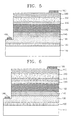
  • FIG. 5 is a sectional view that illustrates a light-emitting device including a p-type electrode structure according to a fifth embodiment of the present invention;
  • FIG. 6 is a sectional view that illustrates a light-emitting device including a p-type electrode structure according to a sixth embodiment of the present invention; and
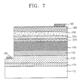
  • FIG. 7 is a sectional view that illustrates a light-emitting device including a p-type electrode structure according to a seventh embodiment of the present invention.
  • Hereinafter, nitride-based light-emitting devices and methods of manufacturing the same according to exemplary embodiments of the present invention will be described in detail with reference to the accompanying drawings.
    The same reference numerals refer to the same constitutional elements throughout the specification.
    FIG. 1 is a sectional view that illustrates a light-emitting device including a p-type electrode structure according to a first embodiment of the present invention.
    Referring to FIG. 1, the light-emitting device of the first embodiment of the present invention has a sequentially stacked structure of a substrate 110, a buffer layer 120, an n-type clad layer 130, an active layer 140, a p-type clad layer 150, and an ohmic contact layer 230. A reference numeral 180 is a p-type electrode pad and a reference numeral 190 is an n-type electrode pad.
    A structure ranging from the substrate 110 to the p-type clad layer 150 corresponds to a light-emitting structure and a structure formed on the p-type clad layer 150 corresponds to a p-type electrode structure.
    Preferably, the substrate 110 is made of one selected from sapphire (Al2O3), silicon carbide (SiC), silicon (Si), and gallium arsenic (GaAs).
    The buffer layer 120 may be omitted.
    The buffer layer 120 through the p-type clad layer 150 are essentially made of a Group III nitride-based compound represented by the formula AlxInyGazN (0≤ x≤ 1, 0≤ y≤ 1, 0≤ z≤ 1, 0≤ x+y+z≤ 1). The n-type clad layer 130 and the p-type clad layer 150 may include an appropriate dopant.
    The active layer 140 may be formed as one of known various structures such as a monolayer or a multiple quantum well (MQW) layer.
    For example, in the case of using a GaN compound, the buffer layer 120 is made of GaN, the n-type clad layer 130 is made of GaN doped with an n-type dopant such as Si, Ge, Se, and Te, the active layer 140 is made of InGaN/GaN MQW or AlGaN/GaN MQW, and the p-type clad layer 150 is made of GaN doped with a p-type dopant such as Mg, Zn, Ca, Sr, and Ba.
    An n-type ohmic contact layer (not shown) may be interposed between the n-type clad layer 130 and the n-type electrode pad 190. The n-type ohmic contact layer may be formed as one of known various structures such as a sequentially stacked structure of titanium (Ti) and aluminum (Al).
    The p-type electrode pad 180 may have a sequentially stacked structure of nickel (Ni)/gold (Au) or silver (Ag)/Au.
    The above-described layers may be formed by e-beam evaporation, PVD (physical vapor deposition), CVD (chemical vapor deposition), PLD (plasma laser deposition), dual-type thermal evaporation, sputtering, or the like.
    The ohmic contact layer 230 is used as a p-type electrode structure and is made of a transparent conductive oxide having a higher work function than 4.7 eV which is the work function of ITO.
    Preferably, the transparent conductive oxide satisfying this requirement is one of first through fourth transparent conductive oxides as will be described later.
    The first transparent conductive oxide has a work function of 5.1 eV and includes gallium (Ga)-indium (In)-oxygen (O) as main components.
    The second transparent conductive oxide has a work function of 5.1 eV and includes zinc (Zn)-indium (In)-oxygen (O) as main components.
    The third transparent conductive oxide has a work function of 5.4 eV and includes gallium (Ga)-indium (In)-tin (Sn)-oxygen (O) as main components.
    The fourth transparent conductive oxide has a work function of 6.1 eV and includes zinc (Zn)-indium (In)-tin (Sn)-oxygen (O) as main components.
    There are no particular limitations on ratios of the main components constituting the first through fourth transparent conductive oxides.
    Preferably, the ohmic contact layer 230 may include at least one metal of the periodic table of elements as a dopant for the transparent conductive oxide to easily form a good ohmic contact with p-type gallium nitride.
    The dopant is used in an amount of 0.01 to 20 wt%, based on the transparent conductive oxide, to allows the ohmic contact layer 230 to have an appropriate electrical property. Here, the term "wt%" indicates a weight ratio of added components.
    Preferably, the ohmic contact layer 230 has a thickness of 1 to 1,000 nm.
    Preferably, the ohmic contact layer 230 is formed by depositing the above-described materials as starting materials using e-beam evaporation, thermal evaporation, sputtering deposition, or pulsed laser deposition.
    The ohmic contact layer 230 is formed at a deposition temperature of 20 to 1,500°C under a deposition pressure of atmospheric pressure to 10-12 torr.
    After forming the ohmic contact layer 230, annealing is performed.
    The annealing is performed in a reactor of 100 to 800°C under vacuum or gas atmosphere for 10 seconds to 3 hours.
    A gas to be supplied to the reactor during the annealing may be at least one selected from nitrogen, argon, helium, oxygen, hydrogen, and air.
    FIG. 2 is a sectional view that illustrates a light-emitting device including a p-type electrode structure according to a second embodiment of the present invention.
    Referring to FIG. 2, the light-emitting device of the second embodiment of the present invention further includes a metal capping layer 240 on the ohmic contact layer 230, as compared to the light-emitting device of the first embodiment of the present invention.
    Here, a p-type electrode structure includes the ohmic contact layer 230 and the metal capping layer 240.
    The metal capping layer 240 is made of a material that can adjust electrical properties (e.g., sheet resistance) of the transparent conductive oxide constituting the ohmic contact layer 230.
    That is, the metal capping layer 240 is made of a material that can form another transparent conductive oxide and facilitate formation of gallide, which is a gallium-based compound, by annealing after deposition, to thereby increase an effective carrier (hole) concentration of a top gallium nitride layer.
    A material for the metal capping layer 240 satisfying the above-described requirements is at least one selected from the group consisting of Ni, NixOy, Au, Pt, Pd, Mg, Cu, CuxOy, Zn, Ag, Sc, Co, CoxOy, Rh, Li, Be, Ca, Ru, Re, Ti, Ta, Na, and La.
    The metal capping layer 240 has a thickness of 1 to 1,000 nm.
    FIG. 3 is a sectional view that illustrates a light-emitting device including a p-type electrode structure according to a third embodiment of the present invention.
    Referring to FIG. 3, the light-emitting device of the third embodiment of the present invention further includes a metal interlayer 220 between the ohmic contact layer 230 and the p-type clad layer 150, as compared to the light-emitting device of the first embodiment of the present invention.
    Here, a p-type electrode structure includes the metal interlayer 220 and the ohmic contact layer 230.
    Preferably, like the above-described metal capping layer 240, the metal interlayer 220 is made of a material that can form another transparent conductive oxide and facilitate formation of gallide which is a gallium-based compound by annealing after deposition to thereby increase an effective carrier (hole) concentration of a top gallium nitride layer.
    A material for the metal interlayer 220 satisfying the above-described requirements is one selected from the group consisting of Ni, NixOy, Au, Pt, Pd, Mg, Cu, CuxOy, Zn, Ag, Sc, Co, CoxOy, Rh, Li, Be, Ca, Ru, Re, Ti, Ta, Na, and La; an alloy or a solid solution of two or more of the forgoing elements; or an oxide of one or more of the forgoing elements.
    The metal interlayer 220 can adjust a carrier concentration of the ohmic contact layer 230 and the p-type clad layer 150, and at the same time, can form another transparent conductive oxide and gallide which is a gallium-based compound by annealing. Therefore, a better ohmic contact with the p-type clad layer 150 can be accomplished.
    Preferably, the metal interlayer 220 has a thickness of 1 to 1,000 nm.
    FIG. 4 is a sectional view that illustrates a light-emitting device including a p-type electrode structure according to a fourth embodiment of the present invention.
    Referring to FIG. 4, the light-emitting device of the fourth embodiment of the present invention includes a reflective layer 250 on the ohmic contact layer 230.
    Here, a p-type electrode structure includes the ohmic contact layer 230 and the reflective layer 250.
    The reflective layer 250 is used to embody a flip-chip light-emitting device and may be made of at least one selected from the group consisting of Ag, Al, Zn, Mg, Ru, Ti, Rh, Cr, and Pt.
    The reflective layer 250 has a thickness of 10 to 2,000 nm.
    The reflective layer 250 may also be added to the light-emitting devices as shown in FIGS. 2 and 3. That is, in the light-emitting device of FIG. 2, the reflective layer 250 may be formed on the metal capping layer 240 using the above-described material. In the light-emitting device of FIG. 3, the reflective layer 250 may be formed on the ohmic contact layer 230 using the above-described material.
    FIG. 5 is a sectional view that illustrates a light-emitting device including a p-type electrode structure according to a fifth embodiment of the present invention.
    Referring to FIG. 5, the light-emitting device of the fifth embodiment of the present invention has a sequentially stacked structure of the reflective layer 250 and a protective layer 260 on the ohmic contact layer 230.
    The protective layer 260 serves to increase adhesion with the p-type electrode pad 180 and increase durability by oxidation prevention of the reflective layer 250 in a flip-chip light-emitting device structure.
    The protective layer 260 is made of one selected from the group consisting of at least one element selected from the group consisting of Au, Ni, Pt, Pd, Cu, and Zn; a compound including the at least one selected from the group consisting of Au, Ni, Pt, Pd, Cu, and Zn; and TiN.
    FIG. 6 is a sectional view that illustrates a light-emitting device including a p-type electrode structure according to a sixth embodiment of the present invention.
    Referring to FIG. 6, the light-emitting device of the sixth embodiment of the present invention has a sequentially stacked structure of the metal capping layer 240, the reflective layer 250, and the protective layer 260, on the ohmic contact layer 230.
    Here, a p-type electrode structure includes the ohmic contact layer 230, the metal capping layer 240, the reflective layer 250, and the protective layer 260.
    The layers as shown in FIG. 6 are made of the above-described materials.
    FIG. 7 is a sectional view that illustrates a light-emitting device including a p-type electrode structure according to a seventh embodiment of the present invention.
    Referring to FIG. 7, the light-emitting device of the seventh embodiment of the present invention further includes the reflective layer 250 and the protective layer 260, as compared with the light-emitting device of FIG. 3.
    The layers as shown in FIG. 7 are made of the above-described materials.
    Meanwhile, the light-emitting devices described with reference to FIGS. 1 through 7 are manufactured by sequentially depositing corresponding layers of a p-type structure on a light-emitting structure ranging from the substrate 110 through the p-type clad layer 150 using a deposition method as described above with reference to FIG. 1 followed by annealing.
    By the annealing, the light-emitting devices can have enhanced current-voltage characteristics.
    As apparent from the above description, according to a nitride-based light-emitting device and a method of manufacturing the same according to the present invention, use of a transparent conductive film electrode layer with a relatively high work function enhances ohmic contact characteristics with a p-type clad layer, thereby ensuring excellent current-voltage characteristics. Furthermore, the high light transmittance of the transparent conductive film electrode layer can increase the emission efficiency of the device.

    Claims (14)

    1. An nitride-based light-emitting device comprising an active layer between an n-type clad layer and a p-type clad layer,
         wherein an ohmic contact layer made of a transparent conductive oxide is formed on the p-type clad layer, and
         the transparent conductive oxide is one selected from the group consisting of a first transparent conductive oxide comprising gallium, indium, and oxygen as main components, a second transparent conductive oxide comprising zinc, indium, and oxygen as main components, a third transparent conductive oxide comprising gallium, indium, tin, and oxygen as main components, and a fourth transparent conductive oxide comprising zinc, indium, tin, and oxygen as main components.
    2. The nitride-based light-emitting device of claim 1, wherein the ohmic contact layer comprises at least one metal as a dopant for the transparent conductive oxide to adjust electrical properties of the ohmic contact layer.
    3. The nitride-based light-emitting device of claim 2, wherein the dopant is used in an amount of 0.001 to 20 wt%, based on the transparent conductive oxide.
    4. The nitride-based light-emitting device of any preceding claim, further comprising a reflective layer made of at least one selected from the group consisting of Ag, Al, Zn, Mg, Ru, Ti, Rh, Cr, and Pt, on the ohmic contact layer.
    5. The nitride-based light-emitting device of claim 4, further comprising a protective layer made of one selected from the group consisting of at least one element selected from the group consisting of Ni, Pt, Pd, Cu, and Zn; a compound comprising the at least one element selected from the group consisting of Ni, Pt, Pd, Cu, and Zn; and TiN.
    6. The nitride-based light-emitting device of any preceding claim, further comprising a metal capping layer made of at least one selected from the group consisting of Ni, NixOy, Au, Pt, Pd, Mg, Cu, CuxOy, Zn, Ag, Sc, Co, CoxOy, Rh, Li, Be, Ca, Ru, Re, Ti, Ta, Na, and La on the ohmic contact layer.
    7. The nitride-based light-emitting device of any preceding claim, further comprising a metal interlayer made of at least one selected from the group consisting of Ni, NixOy, Au, Pt, Pd, Mg, Cu, CuxOy, Zn, Ag, Sc, Co, CoxOy, Rh, Li, Be, Ca, Ru, Re, Ti, Ta, Na, and La, between the p-type clad layer and the ohmic contact layer.
    8. A method of manufacturing a nitride-based light-emitting device having a light-emitting structure comprising an n-type clad layer, an active layer, and a p-type clad layer sequentially stacked on a substrate, the method comprising:
      (a) forming an ohmic contact layer on the p-type clad layer of the light-emitting structure using a transparent conductive oxide; and
      (b) annealing the resultant structure of operation (a),
         wherein in operation (a), the transparent conductive oxide is one selected from the group consisting of a first transparent conductive oxide comprising gallium, indium, and oxygen as main components, a second transparent conductive oxide comprising zinc, indium, and oxygen as main components, a third transparent conductive oxide comprising gallium, indium, tin, and oxygen as main components, and a fourth transparent conductive oxide comprising zinc, indium, tin, and oxygen as main components.
    9. The method of claim 8, wherein the ohmic contact layer comprises at least one metal as a dopant for the transparent conductive oxide to adjust electrical properties of the ohmic contact layer.
    10. The method of claim 9, wherein in operation (a), the dopant is used in an amount of 0.001 to 20 wt%, based on the transparent conductive oxide.
    11. The method of claim 8, 9 or 10, further comprising forming a metal capping layer on the ohmic contact layer using at least one selected from the group consisting of Ni, NixOy, Au, Pt, Pd, Mg, Cu, CuxOy, Zn, Ag, Sc, Co, CoxOy, Rh, Li, Be, Ca, Ru, Re, Ti, Ta, Na, and La.
    12. The method of any of claims 8 to 11, further comprising forming a reflective layer on the ohmic contact layer using at least one selected from the group consisting of Ag, Al, Zn, Mg, Ru, Ti, Rh, Cr, and Pt.
    13. The method of any of claims 8 to 12, further comprising forming a protective layer on the reflective layer using one selected from the group consisting of at least one element selected from the group consisting of Ni, Pt, Pd, Cu, and Zn; a compound comprising the at least one element selected from the group consisting of Ni, Pt, Pd, Cu, and Zn; and TiN.
    14. The method of any of claims 8 to 13, further comprising forming a metal interlayer between the p-type clad layer and the ohmic contact layer using at least one selected from the group consisting of Ni, NixOy, Au, Pt, Pd, Mg, Cu, CuxOy, Zn, Ag, Sc, Co, CoxOy, Rh, Li, Be, Ca, Ru, Re, Ti, Ta, Na, and La.
    EP04256922.8A 2003-11-14 2004-11-09 Nitride-based semiconductor light-emitting device and method of manufacturing the same Expired - Lifetime EP1531499B1 (en)

    Applications Claiming Priority (2)

    Application Number Priority Date Filing Date Title
    KR1020030080719A KR100647279B1 (en) 2003-11-14 2003-11-14 Nitride-based light emitting device and its manufacturing method
    KR2003080719 2003-11-14

    Publications (3)

    Publication Number Publication Date
    EP1531499A2 true EP1531499A2 (en) 2005-05-18
    EP1531499A3 EP1531499A3 (en) 2006-12-20
    EP1531499B1 EP1531499B1 (en) 2014-03-05

    Family

    ID=34431772

    Family Applications (1)

    Application Number Title Priority Date Filing Date
    EP04256922.8A Expired - Lifetime EP1531499B1 (en) 2003-11-14 2004-11-09 Nitride-based semiconductor light-emitting device and method of manufacturing the same

    Country Status (5)

    Country Link
    US (2) US7482639B2 (en)
    EP (1) EP1531499B1 (en)
    JP (1) JP5322367B2 (en)
    KR (1) KR100647279B1 (en)
    CN (1) CN100401539C (en)

    Cited By (3)

    * Cited by examiner, † Cited by third party
    Publication number Priority date Publication date Assignee Title
    DE102005008056A1 (en) * 2004-12-30 2006-07-13 Osram Opto Semiconductors Gmbh Electromagnetic emitting chip has a control layer that allows the level of the emission brightness to be regulated
    US8710486B2 (en) 2007-01-31 2014-04-29 Osram Opto Semiconductors Gmbh Optoelectronic semiconductor chip and method for manufacturing a contact structure for such a chip
    CN113410353A (en) * 2021-04-29 2021-09-17 华灿光电(浙江)有限公司 Light emitting diode epitaxial wafer for improving luminous efficiency and preparation method thereof

    Families Citing this family (26)

    * Cited by examiner, † Cited by third party
    Publication number Priority date Publication date Assignee Title
    KR100638862B1 (en) * 2004-07-12 2006-10-25 광주과학기술원 Flip chip type nitride light emitting device and its manufacturing method
    JP5138873B2 (en) * 2005-05-19 2013-02-06 日亜化学工業株式会社 Nitride semiconductor device
    KR100661711B1 (en) * 2005-08-30 2006-12-26 엘지이노텍 주식회사 A nitride semiconductor light emitting device having a reflective electrode and a method of manufacturing the same
    EP2005488B1 (en) 2005-12-16 2013-07-31 Samsung Display Co., Ltd. Optical device and method of fabricating the same
    KR100784382B1 (en) * 2005-12-16 2007-12-11 삼성전자주식회사 Optical element and its manufacturing method
    US7852610B2 (en) * 2006-01-24 2010-12-14 Fisher Controls International Llc Flameproof apparatus using non-grounded energy-limiting barrier
    DE102006015788A1 (en) * 2006-01-27 2007-09-13 Osram Opto Semiconductors Gmbh Optoelectronic semiconductor chip
    JP5196224B2 (en) * 2006-08-04 2013-05-15 株式会社ナノテコ Method for manufacturing light emitting device
    KR100836494B1 (en) 2006-12-26 2008-06-09 엘지이노텍 주식회사 Semiconductor light emitting device
    CN101308887B (en) * 2007-05-18 2010-09-29 富士迈半导体精密工业(上海)有限公司 High-brightness light-emitting diode and its manufacturing method
    EP2201613A1 (en) * 2007-08-31 2010-06-30 Lattice Power (Jiangxi) Corporation Method for fabricating a low-resistivity ohmic contact to a p-type iii-v nitride semiconductor material at low temperature
    WO2009072365A1 (en) * 2007-12-07 2009-06-11 Idemitsu Kosan Co., Ltd. Amorphous transparent conductive film for gallium nitride compound semiconductor light-emitting device
    CN101960625B (en) * 2008-03-06 2013-01-23 住友金属矿山株式会社 Semiconductor light emitting element, method for manufacturing the semiconductor light emitting element and lamp using the semiconductor light emitting element
    KR101004868B1 (en) 2008-12-17 2010-12-28 고려대학교 산학협력단 Nitride semiconductor light emitting device and manufacturing method
    KR101039946B1 (en) * 2009-12-21 2011-06-09 엘지이노텍 주식회사 Light emitting device, light emitting device package and manufacturing method
    JP5604147B2 (en) * 2010-03-25 2014-10-08 パナソニック株式会社 Transistor and manufacturing method thereof
    TW201349569A (en) * 2012-05-28 2013-12-01 Genesis Photonics Inc Light-emitting element and manufacturing method thereof
    TW201322489A (en) 2011-11-29 2013-06-01 新世紀光電股份有限公司 Light-emitting diode element and flip-chip light-emitting diode package component
    JP6152848B2 (en) * 2012-07-06 2017-06-28 パナソニックIpマネジメント株式会社 Semiconductor light emitting device
    JP2015173229A (en) * 2014-03-12 2015-10-01 沖電気工業株式会社 Transparent electrode structure, nitride semiconductor light emitting diode, and transparent electrode deposition method
    KR102212666B1 (en) * 2014-06-27 2021-02-05 엘지이노텍 주식회사 Light emitting device
    CN108807634A (en) * 2018-07-26 2018-11-13 广东省半导体产业技术研究院 A kind of deep ultraviolet LED structure and preparation method thereof
    CN109037455A (en) * 2018-08-03 2018-12-18 江苏环奥金属材料科技有限公司 A kind of perovskite solar battery and its processing technology
    CN109346562A (en) * 2018-08-30 2019-02-15 华灿光电(浙江)有限公司 A kind of preparation method of light-emitting diode epitaxial wafer and light-emitting diode epitaxial wafer
    CN111864027B (en) * 2019-10-11 2022-09-16 中国科学院宁波材料技术与工程研究所 Ultraviolet LED high-counter electrode, ultraviolet LED and preparation method thereof
    KR20230120175A (en) 2022-02-07 2023-08-17 삼성디스플레이 주식회사 Display device and method of manufacturing the same

    Family Cites Families (25)

    * Cited by examiner, † Cited by third party
    Publication number Priority date Publication date Assignee Title
    JPS5473818A (en) 1977-11-24 1979-06-13 Tokyo Denshi Kagaku Kk Coating solution for forming transparent electric conductive layer and method of coating same
    DE3324647A1 (en) * 1983-07-08 1985-01-17 Schott Glaswerke, 6500 Mainz DIVING METHOD FOR THE PRODUCTION OF TRANSPARENT, ELECTRICALLY CONDUCTIVE, DOPED INDIUMOXIDE LAYERS
    JPH04272612A (en) * 1991-02-26 1992-09-29 Kojundo Chem Lab Co Ltd Transparent electrode
    JPH10341039A (en) 1997-04-10 1998-12-22 Toshiba Corp Semiconductor light emitting device and method of manufacturing the same
    JPH11134112A (en) * 1997-10-28 1999-05-21 Teijin Ltd Input / display integrated device
    JP2000058911A (en) 1998-08-13 2000-02-25 Toshiba Corp Semiconductor light emitting device
    JP3806521B2 (en) * 1998-08-27 2006-08-09 旭硝子セラミックス株式会社 Transparent conductive film, sputtering target, and substrate with transparent conductive film
    JP4559554B2 (en) * 1999-03-05 2010-10-06 出光興産株式会社 Sintered body for sputtering, electron beam and ion plating, and sputtering target
    JP3739951B2 (en) * 1998-11-25 2006-01-25 東芝電子エンジニアリング株式会社 Semiconductor light emitting device and manufacturing method thereof
    US6614059B1 (en) * 1999-01-07 2003-09-02 Matsushita Electric Industrial Co., Ltd. Semiconductor light-emitting device with quantum well
    JP4560149B2 (en) * 1999-03-05 2010-10-13 出光興産株式会社 Transparent conductive material, transparent conductive glass and transparent conductive film
    JP3068914U (en) * 1999-11-11 2000-05-26 洲磊科技股▲ふん▼有限公司 Flip-chip light emitting device
    TW465123B (en) * 2000-02-02 2001-11-21 Ind Tech Res Inst High power white light LED
    US6528340B2 (en) * 2001-01-03 2003-03-04 Honeywell International Inc. Pressure transducer with composite diaphragm
    US6791119B2 (en) * 2001-02-01 2004-09-14 Cree, Inc. Light emitting diodes including modifications for light extraction
    JP2002237215A (en) * 2001-02-08 2002-08-23 Canon Inc Surface-modified transparent conductive film, surface treatment method thereof, and charge injection type light emitting device using the same
    JP4925512B2 (en) * 2001-02-16 2012-04-25 スタンレー電気株式会社 Wavelength conversion type semiconductor device
    JP4302901B2 (en) * 2001-02-27 2009-07-29 三星モバイルディスプレイ株式會社 Luminescent body and light emitting system
    TW492202B (en) * 2001-06-05 2002-06-21 South Epitaxy Corp Structure of III-V light emitting diode (LED) arranged in flip chip configuration having structure for preventing electrostatic discharge
    US20030118865A1 (en) * 2001-08-27 2003-06-26 Marks Tobin J. High work function transparent conducting oxides as anodes for organic light-emitting diodes
    US7148520B2 (en) * 2001-10-26 2006-12-12 Lg Electronics Inc. Diode having vertical structure and method of manufacturing the same
    TW523939B (en) 2001-11-07 2003-03-11 Nat Univ Chung Hsing High-efficient light emitting diode and its manufacturing method
    KR100491968B1 (en) * 2002-03-25 2005-05-27 학교법인 포항공과대학교 Fabrication method of P-type ohmic electrode in gallium nitride based optical device
    JP4233268B2 (en) 2002-04-23 2009-03-04 シャープ株式会社 Nitride-based semiconductor light-emitting device and manufacturing method thereof
    TWI236160B (en) * 2003-11-25 2005-07-11 Super Nova Optoelectronics Cor GaN light emitted diode with high luminescent efficiency and the manufacture method

    Cited By (3)

    * Cited by examiner, † Cited by third party
    Publication number Priority date Publication date Assignee Title
    DE102005008056A1 (en) * 2004-12-30 2006-07-13 Osram Opto Semiconductors Gmbh Electromagnetic emitting chip has a control layer that allows the level of the emission brightness to be regulated
    US8710486B2 (en) 2007-01-31 2014-04-29 Osram Opto Semiconductors Gmbh Optoelectronic semiconductor chip and method for manufacturing a contact structure for such a chip
    CN113410353A (en) * 2021-04-29 2021-09-17 华灿光电(浙江)有限公司 Light emitting diode epitaxial wafer for improving luminous efficiency and preparation method thereof

    Also Published As

    Publication number Publication date
    US20050104077A1 (en) 2005-05-19
    CN1617365A (en) 2005-05-18
    US7964889B2 (en) 2011-06-21
    JP2005150741A (en) 2005-06-09
    US20090095976A1 (en) 2009-04-16
    JP5322367B2 (en) 2013-10-23
    EP1531499A3 (en) 2006-12-20
    KR20050046455A (en) 2005-05-18
    CN100401539C (en) 2008-07-09
    US7482639B2 (en) 2009-01-27
    EP1531499B1 (en) 2014-03-05
    KR100647279B1 (en) 2006-11-17

    Similar Documents

    Publication Publication Date Title
    US7964889B2 (en) Nitride-based light-emitting device and method of manufacturing the same
    US7372081B2 (en) Nitride light emitting device and manufacturing method thereof
    US8395176B2 (en) Top-emitting nitride-based light-emitting device with ohmic characteristics and luminous efficiency
    US7485897B2 (en) Nitride-based light-emitting device having grid cell layer
    US7666693B2 (en) Top-emitting nitride-based light emitting device and method of manufacturing the same
    JP2013065889A (en) Top emit type nitride-based light emitting element
    KR20060007948A (en) Top-Emitt type nitride light emitting device and its manufacturing method
    KR100611642B1 (en) Top-Emitt type nitride light emitting device and its manufacturing method
    KR100611639B1 (en) Top-Emitt type nitride light emitting device and its manufacturing method
    KR100601971B1 (en) Top emitting light emitting device and method of manufacturing thereof
    KR100574105B1 (en) Top-Emitt type nitride light emitting device and its manufacturing method
    KR100574104B1 (en) Flip chip type nitride light emitting device and its manufacturing method
    KR100574103B1 (en) Flip chip type nitride light emitting device and its manufacturing method

    Legal Events

    Date Code Title Description
    PUAI Public reference made under article 153(3) epc to a published international application that has entered the european phase

    Free format text: ORIGINAL CODE: 0009012

    AK Designated contracting states

    Kind code of ref document: A2

    Designated state(s): AT BE BG CH CY CZ DE DK EE ES FI FR GB GR HU IE IS IT LI LU MC NL PL PT RO SE SI SK TR

    AX Request for extension of the european patent

    Extension state: AL HR LT LV MK YU

    PUAL Search report despatched

    Free format text: ORIGINAL CODE: 0009013

    AK Designated contracting states

    Kind code of ref document: A3

    Designated state(s): AT BE BG CH CY CZ DE DK EE ES FI FR GB GR HU IE IS IT LI LU MC NL PL PT RO SE SI SK TR

    AX Request for extension of the european patent

    Extension state: AL HR LT LV MK YU

    17P Request for examination filed

    Effective date: 20070328

    AKX Designation fees paid

    Designated state(s): DE FR GB

    17Q First examination report despatched

    Effective date: 20071106

    RAP1 Party data changed (applicant data changed or rights of an application transferred)

    Owner name: SAMSUNG ELECTRONICS CO., LTD.

    Owner name: GWANGJU INSTITUTE OF SCIENCE AND TECHNOLOGY

    REG Reference to a national code

    Ref country code: DE

    Ref legal event code: R079

    Ref document number: 602004044506

    Country of ref document: DE

    Free format text: PREVIOUS MAIN CLASS: H01L0033000000

    Ipc: H01L0033420000

    GRAP Despatch of communication of intention to grant a patent

    Free format text: ORIGINAL CODE: EPIDOSNIGR1

    RIC1 Information provided on ipc code assigned before grant

    Ipc: H01L 33/42 20100101AFI20131113BHEP

    Ipc: H01L 33/32 20100101ALI20131113BHEP

    INTG Intention to grant announced

    Effective date: 20131205

    GRAS Grant fee paid

    Free format text: ORIGINAL CODE: EPIDOSNIGR3

    GRAA (expected) grant

    Free format text: ORIGINAL CODE: 0009210

    AK Designated contracting states

    Kind code of ref document: B1

    Designated state(s): DE FR GB

    REG Reference to a national code

    Ref country code: GB

    Ref legal event code: FG4D

    REG Reference to a national code

    Ref country code: DE

    Ref legal event code: R096

    Ref document number: 602004044506

    Country of ref document: DE

    Effective date: 20140417

    REG Reference to a national code

    Ref country code: DE

    Ref legal event code: R097

    Ref document number: 602004044506

    Country of ref document: DE

    PLBE No opposition filed within time limit

    Free format text: ORIGINAL CODE: 0009261

    STAA Information on the status of an ep patent application or granted ep patent

    Free format text: STATUS: NO OPPOSITION FILED WITHIN TIME LIMIT

    26N No opposition filed

    Effective date: 20141208

    REG Reference to a national code

    Ref country code: DE

    Ref legal event code: R097

    Ref document number: 602004044506

    Country of ref document: DE

    Effective date: 20141208

    REG Reference to a national code

    Ref country code: FR

    Ref legal event code: PLFP

    Year of fee payment: 12

    REG Reference to a national code

    Ref country code: FR

    Ref legal event code: PLFP

    Year of fee payment: 13

    REG Reference to a national code

    Ref country code: FR

    Ref legal event code: PLFP

    Year of fee payment: 14

    REG Reference to a national code

    Ref country code: FR

    Ref legal event code: PLFP

    Year of fee payment: 15

    PGFP Annual fee paid to national office [announced via postgrant information from national office to epo]

    Ref country code: GB

    Payment date: 20230921

    Year of fee payment: 20

    PGFP Annual fee paid to national office [announced via postgrant information from national office to epo]

    Ref country code: FR

    Payment date: 20230921

    Year of fee payment: 20

    PGFP Annual fee paid to national office [announced via postgrant information from national office to epo]

    Ref country code: DE

    Payment date: 20230926

    Year of fee payment: 20

    REG Reference to a national code

    Ref country code: DE

    Ref legal event code: R071

    Ref document number: 602004044506

    Country of ref document: DE

    REG Reference to a national code

    Ref country code: GB

    Ref legal event code: PE20

    Expiry date: 20241108

    PG25 Lapsed in a contracting state [announced via postgrant information from national office to epo]

    Ref country code: GB

    Free format text: LAPSE BECAUSE OF EXPIRATION OF PROTECTION

    Effective date: 20241108

    PG25 Lapsed in a contracting state [announced via postgrant information from national office to epo]

    Ref country code: GB

    Free format text: LAPSE BECAUSE OF EXPIRATION OF PROTECTION

    Effective date: 20241108