EP1530291A2 - Piezoelektrischer Resonator, piezoelektrisches Filter, Duplexer, Kommunikationsgerät und Herstellungsverfahren des piezoelektrischen Resonators - Google Patents
Piezoelektrischer Resonator, piezoelektrisches Filter, Duplexer, Kommunikationsgerät und Herstellungsverfahren des piezoelektrischen Resonators Download PDFInfo
- Publication number
- EP1530291A2 EP1530291A2 EP04026193A EP04026193A EP1530291A2 EP 1530291 A2 EP1530291 A2 EP 1530291A2 EP 04026193 A EP04026193 A EP 04026193A EP 04026193 A EP04026193 A EP 04026193A EP 1530291 A2 EP1530291 A2 EP 1530291A2
- Authority
- EP
- European Patent Office
- Prior art keywords
- cavity
- piezoelectric
- piezoelectric resonator
- resonance frequency
- substrate
- Prior art date
- Legal status (The legal status is an assumption and is not a legal conclusion. Google has not performed a legal analysis and makes no representation as to the accuracy of the status listed.)
- Withdrawn
Links
Images


Classifications
-
- H—ELECTRICITY
- H03—ELECTRONIC CIRCUITRY
- H03H—IMPEDANCE NETWORKS, e.g. RESONANT CIRCUITS; RESONATORS
- H03H9/00—Networks comprising electromechanical or electro-acoustic elements; Electromechanical resonators
- H03H9/15—Constructional features of resonators consisting of piezoelectric or electrostrictive material
- H03H9/17—Constructional features of resonators consisting of piezoelectric or electrostrictive material having a single resonator
- H03H9/171—Constructional features of resonators consisting of piezoelectric or electrostrictive material having a single resonator implemented with thin-film techniques, i.e. of the film bulk acoustic resonator [FBAR] type
- H03H9/172—Means for mounting on a substrate, i.e. means constituting the material interface confining the waves to a volume
- H03H9/173—Air-gaps
-
- H—ELECTRICITY
- H03—ELECTRONIC CIRCUITRY
- H03H—IMPEDANCE NETWORKS, e.g. RESONANT CIRCUITS; RESONATORS
- H03H3/00—Apparatus or processes specially adapted for the manufacture of impedance networks, resonating circuits, resonators
- H03H3/007—Apparatus or processes specially adapted for the manufacture of impedance networks, resonating circuits, resonators for the manufacture of electromechanical resonators or networks
- H03H3/02—Apparatus or processes specially adapted for the manufacture of impedance networks, resonating circuits, resonators for the manufacture of electromechanical resonators or networks for the manufacture of piezoelectric or electrostrictive resonators or networks
- H03H3/04—Apparatus or processes specially adapted for the manufacture of impedance networks, resonating circuits, resonators for the manufacture of electromechanical resonators or networks for the manufacture of piezoelectric or electrostrictive resonators or networks for obtaining desired frequency or temperature coefficient
-
- H—ELECTRICITY
- H03—ELECTRONIC CIRCUITRY
- H03H—IMPEDANCE NETWORKS, e.g. RESONANT CIRCUITS; RESONATORS
- H03H3/00—Apparatus or processes specially adapted for the manufacture of impedance networks, resonating circuits, resonators
- H03H3/007—Apparatus or processes specially adapted for the manufacture of impedance networks, resonating circuits, resonators for the manufacture of electromechanical resonators or networks
- H03H3/02—Apparatus or processes specially adapted for the manufacture of impedance networks, resonating circuits, resonators for the manufacture of electromechanical resonators or networks for the manufacture of piezoelectric or electrostrictive resonators or networks
- H03H2003/021—Apparatus or processes specially adapted for the manufacture of impedance networks, resonating circuits, resonators for the manufacture of electromechanical resonators or networks for the manufacture of piezoelectric or electrostrictive resonators or networks the resonators or networks being of the air-gap type
Definitions
- the present invention relates to electronic components for use in electronic apparatuses such as mobile telephones, and more particularlyto a piezoelectric resonator,a production method thereof, and a filter, a duplexer, and a communication device, which include the piezoelectric resonator.
- Components included in electronic apparatuses such as mobile devices are required to become more compact and lighter.
- filters for use in mobile devices are required to be compact and accurately adjustable for frequency response.
- a known filter which satisfies the above requirements, includes a piezoelectric resonator (see, for example, pp. 2-4, and FIGS. 3 and 4 of Japanese Laid-Open Patent Publication No. 60-68711).
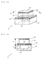
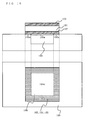
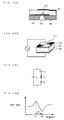
- FIG. 18A is a cross-sectional view showing the basic structure of a conventional piezoelectric resonator.
- the conventional piezoelectric resonator includes a vibration member 710 provided on a substrate 705.
- a cavity 704 is formed by partially etching the substrate 705 from its bottom surface using a micromachining method.
- the vibration member 710 includes a piezoelectric member 701, which is a primary component of the vibration member, and upper and lower electrodes 702 and 703 provided on opposite surfaces of the piezoelectric member 701.
- the reason that the hollow cavity 704 is provided in the substrate 705 is to allow the vibration member 710 to vibrate.
- FIG. 18B is a schematic perspective view used for explaining the operation of the conventional piezoelectric resonator.
- FIG. 18B if an electric field is applied between the upper and lower electrodes 702 and 703, electric energy is converted intomechanicalenergywithinthepiezoelectricmember701, thereby inducing mechanical vibration.
- the induced mechanical vibration expands in the thickness direction, so that the piezoelectric member 701 expands and contracts in the same direction as the electric field is applied.
- v is an average of ultrasonic velocity in materials composing the vibration member 710.
- the piezoelectric member 701 is allowed to vertically vibrate in the thickness direction because the cavity 704 is provided in the substrate 705.
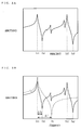
- FIG. 18C is an equivalent circuit diagram of the vibration member 710.
- the equivalent circuit of the vibration member 710 includes a parallel resonance circuit and a series resonance circuit.
- the series resonance circuit includes a capacitor (C1), an inductor (L1), and a resistor (R1)
- the parallel resonance circuit includes a capacitor (C0) connected to the series resonance circuit.
- the vibration member 710 has a resonance frequency and an anti-resonance frequency.
- FIG. 18D is a graph showing frequency characteristics of admittance of the equivalent circuit shown in FIG. 18C.
- the admittance is maximized at a resonance frequency fr1, and minimized at an anti-resonance frequency fa1.
- the resonance frequency fr1 and the anti-resonance frequency fa1 satisfy the following relationships.
- the cavity 704 i.e., a through hole
- the vibration member 710 is partially fixed on the substrate, so that the vibration member 710 is allowed to vertically vibrate in the thickness direction above the cavity.
- the vibration member 710 is partially fixed on the substrate 705, and therefore the vibration member 710 does not entirely generate free vertical vibration in the thickness direction.
- This can be said not onlyof the piezoelectric resonator as shown in FIG. 18A, where the cavity is formed to pass through the bottom surface of the substrate, but also of a piezoelectric resonator in which a cavity is formed by etching a substrate.
- the vibration member 710 is partially fixed on the substrate, therefore the vibration member 710 is inhibited from freely vibrating, or vibration energy is caused to partially leak into the substrate. Accordingly, the conventional piezoelectric resonator has a difficulty in achieving a high Q-factor and a wide frequency range ( ⁇ f) which corresponds to a difference between the resonant frequency and the anti-resonant frequency.
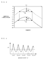
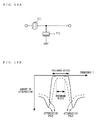
- FIG. 19A is an equivalent circuit diagram of a filter including a piezoelectric resonator.
- the filter shown in FIG. 19A includes a piezoelectric resonator 711 connected in series between input and output terminals, and a piezoelectric resonator 712 connected in parallel between the input and output terminals.
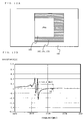
- FIG. 19B is a graph showing band-pass characteristics of the filter shown in FIG. 19A. In FIG. 19B, the horizontal axis indicates frequency, and the vertical axis indicates the amount of attenuation.
- the piezoelectric resonators 711 and 712 each have a narrow frequency range ⁇ f and a low Q-factor.
- the band-pass characteristic of the filter is as indicated by the dotted curve in FIG. 19B. From the dotted curve in FIG. 19B, it is found that in the case of using the piezoelectric resonators 711 and 712 each having a narrow frequency range ⁇ f and a low Q-factor, the passband width of the filter is narrowed, while the loss of the filter is increased. Also, the amount of attenuation at attenuation poles is reduced, resulting in a reduction in steepness of slopes. As such, in the case of using the piezoelectric resonators 711 and 712 each having a narrow frequency range ⁇ f and a low Q-factor, satisfactory filter characteristics cannot be achieved.
- the pass-band characteristic of the filter is as indicated by the solid curve in FIG. 19B. From the solid curve in FIG. 19B, it is found that in the case of using the piezoelectric resonators having a wide frequency range ⁇ f and a high Q-factor, it is possible to increase the passband width of the filter compared to the case of using the piezoelectric resonators having a narrow frequency range ⁇ f and a low Q factor. Also, the loss of the filter is reduced, andthe amount of attenuation at attenuation poles is increased, resulting in an increase in steepness of slopes.
- the present invention has the following features to attain the objects mentioned above.
- the depth t2 of the cavity may be set as shown below, (2 n - 1) ⁇ ⁇ c 4 - ⁇ c 16 ⁇ t 2 ⁇ (2 n - 1) ⁇ ⁇ c 4 + ⁇ c 16 .
- the cavity may be rectangular in cross section.
- a value obtained by dividing an area of a region where an opening of the cavity overlaps the vibration member by an area of a region where the vibration member overlaps the substrate may be equal to or more than 0.5.
- the substrate is etched, and a supporting member is stacked on the substrate, so as to form a cavity having the depth determined by the preliminary step.
- a surface of the substrate may be etched to a depth more than the depth determined by the preliminary step, and an adjustment layer may be provided on the etched surface so as to form a cavity having the depth determined by the preliminary step.
- the present invention provides a filter including a plurality of piezoelectric resonators, at least one of which includes the above features.
- the present invention also provides a duplexer which comprises a filter including a plurality of piezoelectric resonators, at least one of which includes the above features.
- the present invention provides a communication device comprising a piezoelectric resonator including the above features.
- the present invention provides a method for producing a piezoelectric resonator which includes: a substrate; a lower electrode provided on or above the substrate; a piezoelectric member provided on or above the lower electrode; an upper electrode provided on or above the piezoelectric member; and a cavity provided below a vibration member composed of the lowerelectrode, thepiezoelectricmember, andtheupperelectrode, the method comprising a step of determining a depth of the cavity such that a resonance frequency determined by a thickness of the vibration member agrees with a resonance frequency determined by a depth of the cavity.
- the piezoelectric resonator of the present invention it is possible to realize a wide frequency range ⁇ f (a difference between the resonance frequency and the anti-resonance frequency) , and also possible to obtain a high Q-factor.
- the depth t2 of the cavity so as to be equal to (2n-1) ⁇ ⁇ c/4, the width of the frequency range ⁇ f and the Q-factor can be maximized.
- the resonance due to the presence of the cavity is uniquely determined by forming the cavity so as to be rectangular in cross section, therefore it is possible to prevent the occurrence of a spurious resonance frequency, therebyproviding a satisfactory frequency response.
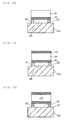
- FIG. 1A is a perspective view of a piezoelectric resonator 1 according to a first embodiment of the present invention.
- FIG. 1B is a cross-sectional view taken along line B-B of FIG. 1A.
- the piezoelectric resonator 1 includes a piezoelectric member 101, an upper electrode 102, a lower electrode 103, a cavity 104, and a substrate 105.
- the lower electrode 103 is formed on the substrate 105, and composed of, for example, molybdenum (Mo), tungsten (W), aluminum (A1) , titanium (Ti), copper (Cu), platinum (Pt), or gold (Au).
- Mo molybdenum
- W tungsten
- Al aluminum
- Ti titanium
- Cu copper
- Pt platinum
- Au gold
- the piezoelectric member 101 is formed on the lower electrode 103, and composed of, for example, a suitable piezoelectric material, such as zinc oxide (ZnO), lead zirconate titanate (PZT), or aluminum nitride (A1N).
- a suitable piezoelectric material such as zinc oxide (ZnO), lead zirconate titanate (PZT), or aluminum nitride (A1N).
- the upper electrode 102 is formed on the piezoelectric member 101, and composed of, for example, molybdenum (Mo) , tungsten (W), aluminum (A1) , titanium (Ti), copper (Cu) , platinum (Pt), or gold (Au).
- Mo molybdenum
- W tungsten
- Al aluminum
- Ti titanium
- Cu copper
- Pt platinum
- Au gold
- the cavity 104 is formed in an upper portion of the substrate 105 underlying the lower electrode 103.
- the cavity 104 has a rectangular shape in cross section.
- the piezoelectric member 101, and the upper and lower electrodes 102 and 103 constitute a vibration member 110 having a thickness t1.
- the cavity 104 has a depth t2.
- FIG. 2A is a graph showing a frequency-admittance characteristic of the piezoelectric resonator 1 in which a resonance frequency caused by vertical vibration (1/2 wavelength mode) of the vibration member 110 in the thickness direction is set so as to be away from a resonance frequency caused by lateral vibration (1/4 wavelength mode) of the cavity 104, thereby causing no interference between the resonance frequencies.
- Resonance and anti-resonance frequencies caused by the vertical vibration (1/2 wavelength mode) of the vibration member 110 in the thickness direction are denoted by fr1 and fa1, respectively.
- Resonance and anti-resonance frequency caused by the lateral vibration (1/4 wavelength mode) of the cavity 104 are denoted by fr2 and fa2, respectively.
- the resonance frequency fr1 caused by the vertical vibration of the vibration member 110 in the thickness direction depends on the thickness of the vibrationmember 110 .
- the resonance frequency fr2 caused by the lateral vibration of the cavity 104 depends on the depth of the cavity 104.
- the resonance frequency fr1 is not affected by the resonance frequency fr2 if it is sufficiently away from the resonance frequency fr2.
- the resonance frequency fr2 is not affected by the resonance frequency fr1 if it is sufficiently away from the resonance frequency fr1.
- FIG. 2B is a graph in which the dotted curve indicates a frequency-admittance characteristic of the piezoelectric resonator 1 in the case where the resonance frequency fr2 is equal to the resonance frequency fr1, and the solid curve indicates the same frequency-admittance characteristic as that shown in FIG. 2A.
- the depth t2 of the cavity is adjusted such that the resonance frequency fr2 approximates the resonance frequency fr1, a frequency range ⁇ f is widened and the Q-factor is increased. Accordingly, if the resonance frequency fr1 and the resonance frequency fr2 are equal to each other, it is possible to achieve the widest frequency range ⁇ f and the highest Q-factor.
- the vertical vibration mode of the vibration member 110 in the thickness direction is coupled with the lateral vibration of the cavity 14, so that a new anti-resonance frequency fb occurs as indicated by the dotted curve shown in FIG. 2B.
- the frequency range ⁇ f which corresponds to a difference between the resonance frequency fr1 and the anti-resonance frequency fb, is widened. It is appreciated that the frequency range ⁇ f is wide compared to a frequency range ⁇ fa corresponding to a difference between the resonance frequency fr1 and the anti-resonance frequency fa1.
- FIG. 3 is a graph showing relationships between frequencies and the amount of attenuation in the vicinity of the resonance frequency fr1 shown in FIG. 2B.
- the dotted curve shows a characteristic in the case where the resonance frequencies fr1 and fr2 are equal to each other (the dotted curve of FIG. 2B)
- the solid curve shows a characteristic in the case where the resonance frequencies fr1 and fr2 are set so as to be away from each other, thereby causing no interference between the resonance frequencies (the solid curve of FIG. 2B).
- a frequency width H1 which corresponds to a 3-dB loss from the vertex of the characteristic shown by the dotted curve
- a frequency width H2 which corresponds to a 3-dB loss from the vertex of the characteristic shown by the solid curve. Accordingly, it can be said that the Q-factor of the characteristic shown by the dotted curve is higher than the Q-factor of the characteristic shown by the solid curve.
- the reason for this is that in the case of calculating the Q-factor, a frequency width corresponding to a 3-dB loss from the vertex of a resonance point is used as a denominator, and therefore the Q-factor becomes higher as the frequency width corresponding to a 3-dB loss becomes narrower.
- a high Q-value is achieved when the resonance frequencies fr1 and fr2 are equal to each other.
- the wavelength ⁇ c of vibration caused in the cavity 104 due to vibration of the vibration member 110 is determined based on the resonance frequency fr1 and the average of ultrasonic velocity Vs2 in the material of the substrate 105 having the cavity 104 formed therein, and therefore can be given by the following expression (4).
- ⁇ c V s 2 f r 1
- the depth t2 of the cavity 104 can be expressed by the following expression (5).
- t 2 ⁇ c 4
- the bottom surface of the cavity 104 is fixed if the resonance frequencies fr1 and fr2 are equal to each other.
- the vertical vibration of the vibration member 110 in the thickness direction and the lateral vibration of the cavity 104 are confined in the vibration member 110 and the cavity 104. Consequently, the vertical vibration of the vibration member 110 in the thickness direction is less affected by a support member for supporting the vibration member 110 on the substrate 105, and therefore the vibration member 110 vertically vibrates in the thickness direction almost freely, making it possible to achieve a wide frequency range ⁇ f. Also, the loss is reduced, resulting in an increase of the Q-factor.
- FIG. 4 is a graph showing variations of a frequency range ⁇ f with respect to the depth t2 of the cavity 104.
- the frequency range ⁇ f is maximized when the depth t2 of the cavity 104 is an odd multiple of ⁇ c/4. This is because in the case where the depth t2 of the cavity 104 is an odd multiple of ⁇ c/4, the bottom surface of the cavity 104 is fixed. Accordingly, the expression (5) can be generalized to the following expression (6).
- t 2 (2n - 1) ⁇ ⁇ c 4 ; (where n is an integer)
- the depth t2 of the cavity 104 satisfies the expression (6), it is possible to achieve a wide frequency range ⁇ f and a high Q-factor.
- Table 1 below shows frequency ranges ⁇ f in association with changes of the depth of the cavity 104 from ⁇ c/4 in the case where the center frequency (the resonance frequency of the vibration member 20) is either at 1 GHz or at 10 GHz.
- Table 1 also shows, for comparison purposes, frequency ranges ⁇ f for a conventional structure where the cavity 104 of the piezoelectric resonator 1 shown in FIG. 1 passes through the bottom surface of the substrate 15.
- Table 2 below shows frequency ranges ⁇ f in association with changes of the depth of the cavity 104 from 3 ⁇ c/4 in the case where the center frequency (the resonance frequency of the vibration member 20) is either at 1 GHz or at 10 GHz.
- Table 2 also shows, for comparison purposes, frequency ranges ⁇ f for a conventional structure where the cavity 104 of the piezoelectric resonator 1 shown in FIG. 1 passes through the bottom surface of the substrate 15.
- Tables 1 and 2 have a "Grades" field which shows whether achieved frequency ranges ⁇ f are wider than those achieved in the conventional structure.
- Grades A to C indicate that achieved frequency ranges ⁇ f are wider than those achieved in the conventional structure.
- Grade D indicates that achieved frequency ranges ⁇ f are narrower than those achieved in the conventional structure.
- Grade A indicates the widest frequency ranges ⁇ f
- Grade B indicates frequency ranges ⁇ f narrower than those in Grade A but wider than those in Grade C
- Grade C indicates frequency ranges ⁇ f narrower than those in Grade B but wider than those in Grade D.
- the depth t2 of the cavity 104 is set within a range of ⁇ c/16 with respect to an oddmultiple of ⁇ c/4 as expressed by expression (8) below, whereby it is possible to achieve a further wider frequency range ⁇ f. (2 n - 1) ⁇ ⁇ c 4 - ⁇ c 16 ⁇ t 2 ⁇ (2 n - 1) ⁇ ⁇ c 4 + ⁇ c 16
- FIGS. 5A through 5G are views used for explaining the method for producing a piezoelectric resonator.
- the area of a top surface of a lower electrode is the same as a base area of a piezoelectric member.
- elements having functions similar to those of elements shown in FIGs. 1A and 1B are denoted by the same reference numerals.
- a substrate 105a is prepared.
- a preliminary step is carried out to determine the depth t2 of the cavity 104 so as to satisfy the condition of the expression (6), (7), or (8).
- the resonance frequency fr is calculated based on the thickness of the vibration member 110
- the average of ultrasonic velocity Vc2 in the material of the substrate 105 having the cavity 104 formed therein is calculated, and then the wavelength ⁇ c is calculated by expression (4).
- the depth t2 of the cavity 104 is determined so as to satisfy the condition of the expression (6), (7) , or (8).
- the substrate 105a is etched to the determined depth t2, thereby forming the substrate 105 having the cavity 104 formed therein.
- the cavity 104 is filled with a sacrificial layer 106 to be removed later.
- the sacrificial layer 106 is composed of, for example, a readily soluble material such as phosphosilicate glass (PSG).
- the lower electrode 103 is formed on the substrate 105 so as to cover the top of the cavity 104.
- the piezoelectric member 101 is deposited on the lower electrode 103.
- the deposition is carried out by, for example, a sputtering method or a CVD method.
- the upper electrode 102 is formed on the piezoelectric member 101, thereby completing the vibration member 110.
- the sacrificial layer 106 is removed from the cavity 104.
- the removal of the sacrificial layer 106 is carried out by dissolution with an aqueous solution of hydrogen fluoride or by another method.
- the structure of a piezoelectric resonator of the present invention is not limited to that described in the first embodiment. Variations of the structure will be described in a second embodiment of the present invention.
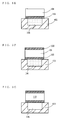
- FIG. 6A is a cross-sectional view showing the structure of a piezoelectric resonator in which a cavity is formed byproviding a supporting member.
- a support member 207 is formed on the substrate 105a so as to form a cavity 204.
- the lower electrode 103 is formed on the supporting member 207 above the substrate 105a.
- a wide frequency range ⁇ f and a high Q-factor can also be achieved by determining the depth of the cavity so as to satisfy the expression (6), (7), or (8) .
- the cavity 204 is formedbydepositing the supporting member 207, the depth of the cavity 204 can be accuratelyadjusted, achievinghighproductionefficiency.
- the supporting member 207 is composed of a material with high acoustic impedance, it is possible to increase the freedom in selecting the material of the substrate 105, while achieving an effect of reducing a spurious resonance frequency.
- FIG. 6B is a cross-sectional view showing the structure of a piezoelectric resonator in which a cavity is formed by etching a substrate surface and providing a supporting member.
- a surface of a substrate 105b is etched to form a recess portion 214b, and then a supporting member 217 is formed, thereby forming a cavity portion 214a.
- the recess portion 214b and the cavity portion 214a constitute a cavity 214.
- a wide frequency range ⁇ f and a high Q-factor can also be achieved by determining the depth of the cavity so as to satisfy the expression (6), (7), or (8).
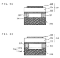
- FIG. 6C is a cross-sectional view showing the structure of a piezoelectric resonator obtained by replacing the vibration member 110 of the piezoelectric resonator shown in FIGs. 1A and 1B with a vibration member 210 in which a top surface of a piezoelectric member 231 and a bottom surface of an upper electrode 232 are different in size from each other.
- FIG. 6D is a cross-sectional view showing the structure of a piezoelectric resonator obtained by replacing the vibration member 110 of the piezoelectric resonator shown in FIG. 6A with the vibration member 210 in which the top surface of the piezoelectric member 231 and the bottom surface of the upper electrode 232 are different in size from each other.
- FIG. 6C is a cross-sectional view showing the structure of a piezoelectric resonator obtained by replacing the vibration member 110 of the piezoelectric resonator shown in FIG. 6A with the vibration member 210 in which the top surface of the piezoelectric member 2
- FIG. 6E is a cross-sectional view showing the structure of a piezoelectric resonator obtained by replacing the vibration member 110 of the piezoelectric resonator shown in FIG. 6B with the vibration member 210 in which the top surface of the piezoelectric member 231 and the bottom surface of the upper electrode 232 are different in size from each other.
- a wide frequency range ⁇ f and a high Q-factor can also be achieved by determining the depth of the cavity 234, 204, or 214 so as to satisfy the expression (6), (7), or (8), and by forming the vibration member 210, as shown in FIGs. 6C, 6D, and 6E, such that the top surface of the piezoelectric member 231 differs in size from the bottom surface of the upper electrode 232 and the bottom surface of the piezoelectric member 231 is equal in size to the top surface of the lower electrode 233.
- the wavelength ⁇ c is determined based on the average of ultrasonic velocity in the material of the substrate having the cavity formed therein and the resonance frequency of the vibration member.
- FIGS. 6A through 6E elements having similar functions are denoted by the same reference numerals (this is also true of other figures). Also, elements having functions similar to those of elements shown in FIGs. 1A and 1B are denoted by the same reference numerals (this is also true of other figures).
- FIGS. 7A through 7G are views used for explaining a method for producing the piezoelectric resonator shown in FIG. 6A in accordance with a third embodiment of the present invention.
- the method for producing the piezoelectric resonator shown in FIG. 6A is described with reference to FIGs. 7A through 7G.
- the substrate 105a is prepared.
- a preliminary step is carried out to determine the depth t2 of the cavity 204 so as to satisfy the condition of the expression (6), (7), or (8).
- the resonance frequency fr is calculated based on the thickness of the vibration member 110
- the average of ultrasonic velocity Vc2 in the material of the substrate 105a having the cavity 204 formed therein is calculated, and then the wavelength ⁇ c is calculated by expression (4).
- the depth t2 of the cavity 204 is determined so as to satisfy the condition of the expression (6), (7), or (8) .
- the height of the supporting member 207 is determined so as to be equal to the determined cavity depth.
- the supporting member 207 is formed on the top surface of the substrate 105a so as to have a height as determined.
- the supporting member 207 is filled with a sacrificial layer 306 to be removed later.
- the sacrificial layer 306 is composed of, for example, a readily soluble material such as phosphosilicate glass (PSG).
- the lower electrode 103 is formed on the substrate 105a so as to cover the top of the supporting member 207.
- the piezoelectric member 101 is deposited on the lower electrode 103 above the supporting member 207 and the sacrificial layer 306.
- the deposition is carried out by, for example, a sputtering method or a CVD method.
- the upper electrode 102 is formed on the piezoelectric member 101.
- the sacrificial layer 306 is removed, thereby exposing the cavity 204.
- the removal of the sacrificial layer 306 is carried out by dissolution with an aqueous solution of hydrogen fluoride or by another method.
- the third embodiment it is possible to provide a piezoelectric resonator, which achieves a wide frequency range ⁇ f and a high Q-factor, by simply carrying out steps of determining the depth t2 of the cavity so as to satisfy the condition of the expression (6) , (7) , or (8) , and forming the supporting member having a height equal to the determined cavity depth. Accordingly, no additional process is required for widening the frequency range ⁇ f and increasing the Q-value, therefore it is possible to simplify the production process.
- FIGs. 8A through 8G are views used for explaining a method for producing the piezoelectric resonator shown in FIG. 6B in accordance with a fourth embodiment of the present invention.
- the method for producing the piezoelectric resonator shown in FIG. 6B is described with reference to FIGS. 8A through 8G.
- the substrate 105 is prepared.
- a preliminary step is carried out to determine the depth t2 of the cavity 214 so as to satisfy the condition of the expression (6), (7), or (8).
- the resonance frequency fr is calculated based on the thickness of the vibration member 110
- the average of ultrasonic velocity Vc2 in the material of the substrate 105 having the cavity 214 formed therein is calculated, and then the wavelength ⁇ c is calculated by expression (4).
- the depth t2 of the cavity 214 is determined so as to satisfy the condition of the expression (6), (7), or (8) .
- the determined cavity depth is referred to as a "set value".
- the top surface of a substrate 115 is etched to form the substrate 105b and the recess portion 214b.
- the supporting member 217 is formed around the etched region.
- the height of the supporting member 217 is adjusted such that the depth of the cavity 214 composed of the recess portion 214b and the cavity portion 214a becomes equal to the set value.
- the sacrificial layer 406a is composed of, for example, a readily soluble material such as phosphosilicate glass (PSG).
- the lower electrode 103 is formed so as to cover the top of the supporting member 217 and the top of the sacrificial layer 406a in the cavity 214.
- the piezoelectric member 101 is deposited on the lower electrode 103, and the upper electrode 102 is deposited on the piezoelectric member 101.
- the deposition is carried out by, for example, a sputtering method or a CVD method.
- the sacrificial layer 406a is removed, thereby exposing the cavity 214.
- the removal of the sacrificial layer 406a is carried out by dissolution with an aqueous solution of hydrogen fluoride or by another method.
- the fourth embodiment it is possible to provide a piezoelectric resonator, which achieves a wide frequency range ⁇ f and a high Q-factor, by simply carrying out steps of determining the depth t2 of the cavity 214 so as to satisfytheconditionoftheexpression (6), (7), or (8), andforming the supporting member 217 having a height equal to the determined cavity depth. Accordingly, no additional process is required for widening the frequency range ⁇ f and increasing the Q-value, therefore it is possible to simplify the production process.
- piezoelectric resonators shown in FIGs. 6C, 6D, and 6E can be produced by the production methods described in conjunction with FIGS. 6A through 8G if the lower electrode and the piezoelectric member are changed in size.
- a piezoelectric resonator according to a fifth embodiment of the present invention differs from the piezoelectric resonator according to the first embodiment in that an adjustment layer for adjusting a cavity depth is provided on the bottom of a cavity formed by etching a substrate.
- FIGs. 9A through 9H are views used for explaining a method for producing the piezoelectric resonator according to the fifth embodiment.
- the method for producing the piezoelectric resonator according to the fifth embodiment is described with reference to FIGs. 9A through 9H.
- the substrate 115 is prepared.
- a preliminary step is carried out to determine the depth t2 of a cavity 504b so as to satisfy the condition of the expression (6), (7), or (8).
- the resonance frequency fr is calculated based on the thickness of the vibration member 110
- the average of ultrasonic velocity Vc2 in the material of the substrate 115 having the cavity 504b formed therein is calculated, and then the wavelength ⁇ c is calculated by expression (4).
- the depth t2 of the cavity 504b is determined so as to satisfy the condition of the expression (6), (7), or (8) .
- the determined cavity depth is referred to as a "set value".
- the substrate 115 is partially etched to form a recess portion 504.
- the depth of the recess portion 504 is greater than the set value.
- a cavity depth adjustment layer 504a is formed on the bottom of the recess portion 504.
- the thickness of the cavity depth adjustment layer 504a is adjusted such that the depth of the cavity 504b becomes equal to the set value.
- the sacrificial layer 506 is composed of, for example, a readily soluble material such as phosphosilicate glass (PSG).
- the lower electrode 103 is deposited so as to cover the top of the sacrificial layer 506 in the cavity 504b.
- the piezoelectric member 101 is deposited on the lower electrode 103.
- the upper electrode 102 is deposited on the piezoelectric member 101.
- the deposition is carried out by, for example, a sputtering method or a CVD method.
- the sacrificial layer 506 is removed, thereby exposing the cavity 504b.
- the removal of the sacrificial layer 506 is carried out by dissolution with an aqueous solution of hydrogen fluoride or by another method.
- the fifth embodiment it is possible to provide a piezoelectric resonator, which achieves a wide frequency range ⁇ f and a high Q-factor, by simply carrying out steps of determining the depth t2 of the cavity 504b so as to satisfy the condition of the expression (6), (7), or (8), and forming the adjustment layer 504a, thereby forming the cavity 504b having a predetermined depth. Accordingly, no additional process is required for widening the frequency range ⁇ f and increasing the Q-value, therefore it is possible to simplify the production process.
- examples of designing a cavity depth are described with illustration of materials of a substrate having a cavity formed therein.
- Table 3 below shows ranges of the depth of the cavity in the case where Si, SiO2, or SiN is used as the material of the substrate and the resonance frequency is at 2 GHz.
- the density of the material and Young's modulus are used to derive the average of ultrasonic velocity in the material, and thereby to readily determine the depth of a cavity.
- the depth of a cavity for the desired resonance frequency can be obtained by multiplying the cavity depth shown in Table 3 by 2/f GHz.
- the desired resonance frequency f is 4 GHz
- the depth of a cavity therefor can be obtained by multiplying the cavity depth shown in Table 3 by 2/4 GHz.
- the cavity depth is in the following ranges: 0.21-0.63, 1.06-1.47, 1.91-2.31, ... .
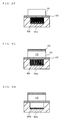
- FIG. 10 shows cross-sectional and top views of a piezoelectric resonator.
- degree ⁇ of overlap between the cavity and the vibration member is described with reference to FIG. 10.
- the lower electrode 103 is provided in a size corresponding to the bottom surface of the piezoelectric member 101.
- the seventh embodiment is applicable to the case as shown in FIG. 1A, where the lower electrode is provided on the entire top surface of the substrate 105.
- an opening 104a of the cavity which overlaps the vibration member, has an area of A.
- a region corresponding to the area of A is indicated by a dotted square.
- a region 103a, where the lower electrode 103 overlaps the substrate 105 has an area of B. More specifically, in the region 103a, the vibration member consisting of the piezoelectric member 101, the upper electrode 102, and the lower electrode 103 overlap the substrate 105.
- the area of B of the region 103a, where the vibration member overlaps the substrate 105 corresponds to the size of an area remaining after the area of A of the opening 104a of the cavity is subtracted from the base area of the vibration member, i.e., the base area of the lower electrode 105.
- the region corresponding to the area of B is hatched by horizontal wavy lines.
- FIG. 11 is a graph showing a frequency-susceptance characteristic of the piezoelectric resonator shown in FIG. 10.
- FIG. 12B is a graph showing a frequency-susceptance characteristic of the piezoelectric resonator shown in FIG. 12A.
- FIG. 13B is a graph showing a frequency-susceptance characteristic of the piezoelectric resonator shown in FIG. 13A.
- FIG. 14B is a graph showing a frequency-susceptance characteristic of the piezoelectric resonator shown in FIG. 14A.
- the spurious resonance frequency slightly exists between the resonance frequency fr and the anti-resonance frequency fa.
- the frequency range ⁇ f has a width of 42.9 [MHz].
- the value ⁇ which is obtained by dividing the area of A of the region where the opening of the cavity overlaps the vibration member by the area of B of the region where the vibration member overlaps the substrate, is equal to or more than 0.5, it is possible to provide a piezoelectric resonator in which no spurious resonance frequency occurs between the resonance frequency and the anti-resonance frequency
- the cavity is rectangular in cross section, i.e., the cavity has perpendicular walls. This is because in the case of the rectangular cross-sectional shape (perpendicular walls), it is possible to readily cause the resonance frequency of the vibration member and the resonance frequency of the cavity to agree with each other.
- the cavity does not have to be rectangular in cross section so long as the expression (7) is satisfied.
- the cavity may be trapezoidal in cross section, and the cavity walls may be inclined.
- the piezoelectric member is provided on the lower electrode so as to be in close contact therewith.
- a dielectric member may be provided between the lower electrode and the piezoelectric member. That is, the piezoelectric member may be formed on or above the lower electrode.
- the dielectric member may be provided between the piezoelectric member and the upper electrode. That is, the upper electrode may be formed on or above the piezoelectric member.
- the resonance frequency fr is determined by the thickness of the vibration member including the dielectric member.
- the piezoelectric member may be composed of a single-crystal bulk, rather than a film bulk material.
- the cavity walls and/or the supporting member are each composed of a plurality of materials, an average of ultrasonic velocity in the materials are used for calculating the vibration wavelength ⁇ c.
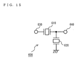
- FIG. 15 is a diagram showing a structure of a ladder filter 600 according to an eighth embodiment of the present invention.
- the ladder filter 600 includes a first piezoelectric resonator 610, a second piezoelectric resonator 620, and input/output terminals 630 and 640.
- the first and second piezoelectric resonators 610 and 620 have a cavity which satisfies requirements as described in the first through third embodiment.
- the first piezoelectric resonator 610 is connected in series between the input/output terminals 630 and 640. Accordingly, the first piezoelectric resonator 610 operates as a series resonator.
- the second piezoelectric resonator 620 is connected in parallel between the input/output terminals 630 and 640, and is grounded at one end. Accordingly, the second piezoelectric resonator 620 operates as a parallel resonator.
- a ladder filter of an L-shaped configuration is provided by connecting piezoelectric resonators in a manner as described above.
- a resonance frequency of the first piezoelectric resonator 610 and a resonance frequency of the second piezoelectric resonator 620 are set so as to differ from each other. Specifically, the resonance frequency of the first piezoelectric resonator 610 is set so as to be higher than the resonance frequency of the second piezoelectric resonator 620. This realizes a ladder filter having a bandpass characteristic. Preferably, the resonance frequency of the first piezoelectric resonator 610 is set so as to be equal or close to an anti-resonance frequency of the second piezoelectric resonator 620, thereby realizing a ladder filter having a satisfactorily flatter bandpass.
- the thickness of the vibration member may be adjusted in order to configure a piezoelectric resonator having a desired resonance frequency.
- the piezoelectric resonator of the present invention may be applied to a multistage ladder filter.
- an effect similar to that achieved by the filter of an L-shaped configuration can be achieved by a ladder filter of, for example, a T- or n-shaped configuration. It goes without saying that the similar effect can be achieved by a multistage filter of a T- or n-shaped configuration.
- a lattice filter can also achieve an effect similar to that achieved by a ladder filter.
- the present invention is not limited to the above configuration, and any configuration can be used so long as the filter includes at least one piezoelectric resonator of the present invention.
- a ninth embodiment of the present invention is described with respect to structures of an antenna duplexer which includes piezoelectric resonators of the present invention.
- FIG. 16 is a diagram showing an exemplary structure of an antenna duplexer 400 according to the ninth embodiment of the present invention.
- the antenna duplexer 400 includes a Tx filter (transmission filter) 401, an Rx filter (reception filter) 402, and a phase-shift circuit 403.
- the Tx filter 401 and the Rx filter 402 include piezoelectric resonators of the present invention.
- the phase-shift circuit 403 consists of two transmission lines.
- the Tx filter 401 passes signals in a transmission frequency band, and attenuates signals in a reception frequency band.
- the Rx filter 402 passes signals in the reception frequency band, and attenuates signals in the transmission frequency band.
- the antenna duplexer is not limited by FIG. 11 in terms of the number of filters and the number of stages of the piezoelectric resonators included in the filters, and can be freely designed.
- at least one of the piezoelectric resonators included in the Tx filter 401 and/or the Rx filter 402 may be a piezoelectric resonator of the present invention.
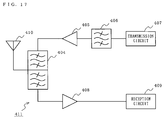
- FIG. 17 is a diagram showing an exemplary structure of a communication device 411 according to a tenth embodiment of the present invention.
- the communication device 411 includes an antenna duplexer 404, which is the same as that shown in FIG. 16, a transmission amplifier 405, a filter 406, a transmission circuit 407, a reception amplifier 408, a reception circuit 409, and an antenna 410.
- a transmission signal outputted by the transmission circuit 407 is inputted to the antenna duplexer 404 via the filter 406 and the transmission amplifier 405.
- the transmission signal inputted to the antenna duplexer 404 is transmitted via the antenna 410.
- a reception signal received by the antenna 410 is inputted to the reception circuit 409 via the antenna duplexer 404 and the reception amplifier 408.
- the piezoelectric resonator of the present invention may be used in the filter 406.
- the communication device is not limited to that shown in FIG. 17, and can be freely designed.
- the piezoelectric resonator of the present invention can be used not only in the duplexer or a filter at a transmission end and may be used in a filter at a reception end.
- piezoelectric resonators of the present invention are used in an antenna duplexer or a communication device, thereby realizing an antenna duplexer or communication device having satisfactory characteristics.
- a piezoelectric resonator of the present invention achieves a wide frequency range ⁇ f and a high Q-factor, and therefore is advantageous if used in, for example, a mobile telephone, wireless communication, or wireless internet connection.
Landscapes
- Physics & Mathematics (AREA)
- Acoustics & Sound (AREA)
- Engineering & Computer Science (AREA)
- Manufacturing & Machinery (AREA)
- Piezo-Electric Or Mechanical Vibrators, Or Delay Or Filter Circuits (AREA)
Applications Claiming Priority (2)
| Application Number | Priority Date | Filing Date | Title |
|---|---|---|---|
| JP2003378257 | 2003-11-07 | ||
| JP2003378257 | 2003-11-07 |
Publications (1)
| Publication Number | Publication Date |
|---|---|
| EP1530291A2 true EP1530291A2 (de) | 2005-05-11 |
Family
ID=34431340
Family Applications (1)
| Application Number | Title | Priority Date | Filing Date |
|---|---|---|---|
| EP04026193A Withdrawn EP1530291A2 (de) | 2003-11-07 | 2004-11-04 | Piezoelektrischer Resonator, piezoelektrisches Filter, Duplexer, Kommunikationsgerät und Herstellungsverfahren des piezoelektrischen Resonators |
Country Status (4)
| Country | Link |
|---|---|
| US (1) | US7230367B2 (de) |
| EP (1) | EP1530291A2 (de) |
| KR (1) | KR20050044291A (de) |
| CN (1) | CN1614876A (de) |
Families Citing this family (11)
| Publication number | Priority date | Publication date | Assignee | Title |
|---|---|---|---|---|
| US7113055B2 (en) * | 2003-11-07 | 2006-09-26 | Matsushita Electric Industrial Co., Ltd. | Piezoelectric resonator, method of manufacturing piezoelectric resonator, and filter, duplexer, and communication device using piezoelectric resonator |
| JP5089860B2 (ja) * | 2004-12-03 | 2012-12-05 | 富士フイルム株式会社 | 圧電アクチュエータ及び液体吐出ヘッド |
| JP2006217281A (ja) * | 2005-02-03 | 2006-08-17 | Toshiba Corp | 薄膜バルク音響装置の製造方法 |
| US20060274476A1 (en) * | 2005-04-13 | 2006-12-07 | Andrew Cervin-Lawry | Low loss thin film capacitor and methods of manufacturing the same |
| EP1887688A4 (de) * | 2005-06-02 | 2009-08-05 | Murata Manufacturing Co | Piezoelektrischer resonator und piezoelektrischer dünnschichtfilter |
| US20070063777A1 (en) * | 2005-08-26 | 2007-03-22 | Mircea Capanu | Electrostrictive devices |
| JP4252584B2 (ja) | 2006-04-28 | 2009-04-08 | 富士通メディアデバイス株式会社 | 圧電薄膜共振器およびフィルタ |
| EP2815638B1 (de) * | 2012-04-03 | 2016-08-24 | Siemens Aktiengesellschaft | Kühlvorrichtung |
| US12155362B2 (en) * | 2019-09-05 | 2024-11-26 | Changzhou Chemsemi Co., Ltd. | Method for forming bulk acoustic wave resonance device |
| CN111294010B (zh) * | 2020-02-15 | 2023-08-25 | 见闻录(浙江)半导体有限公司 | 一种薄膜体声波谐振器的腔体结构及制造工艺 |
| CN115051679A (zh) * | 2021-03-08 | 2022-09-13 | 诺思(天津)微系统有限责任公司 | 谐振器及其制造方法、滤波器及电子设备 |
Family Cites Families (5)
| Publication number | Priority date | Publication date | Assignee | Title |
|---|---|---|---|---|
| JPS6068711A (ja) | 1983-09-26 | 1985-04-19 | Toshiba Corp | 圧電薄膜共振子 |
| JPS6068710A (ja) | 1983-09-26 | 1985-04-19 | Toshiba Corp | 圧電薄膜共振子 |
| US6349454B1 (en) * | 1999-07-29 | 2002-02-26 | Agere Systems Guardian Corp. | Method of making thin film resonator apparatus |
| KR100398363B1 (ko) | 2000-12-05 | 2003-09-19 | 삼성전기주식회사 | Fbar 소자 및 그 제조방법 |
| JP3939939B2 (ja) | 2001-07-17 | 2007-07-04 | 富士通株式会社 | 圧電薄膜共振素子の製造方法 |
-
2004
- 2004-11-03 US US10/979,277 patent/US7230367B2/en not_active Expired - Fee Related
- 2004-11-04 EP EP04026193A patent/EP1530291A2/de not_active Withdrawn
- 2004-11-05 KR KR1020040089844A patent/KR20050044291A/ko not_active Withdrawn
- 2004-11-08 CN CNA2004100905575A patent/CN1614876A/zh active Pending
Also Published As
| Publication number | Publication date |
|---|---|
| US7230367B2 (en) | 2007-06-12 |
| US20050099093A1 (en) | 2005-05-12 |
| KR20050044291A (ko) | 2005-05-12 |
| CN1614876A (zh) | 2005-05-11 |
Similar Documents
| Publication | Publication Date | Title |
|---|---|---|
| US11699988B2 (en) | Resonator and method for manufacturing the same | |
| US10700660B2 (en) | Bulk acoustic wave resonator | |
| US7388318B2 (en) | Thin film piezoelectric resonator, thin film piezoelectric device, and manufacturing method thereof | |
| KR100799391B1 (ko) | 박막 음향공진기 및 그 제조방법 | |
| US6448695B2 (en) | Bulk acoustic wave device | |
| KR100488617B1 (ko) | 압전 공진기, 필터 및 전자 통신 장치 | |
| US6812619B1 (en) | Resonator structure and a filter comprising such a resonator structure | |
| US7508286B2 (en) | HBAR oscillator and method of manufacture | |
| US20050168102A1 (en) | Film bulk acoustic wave resonator, film bulk acoustic wave resonator filter and method of manufacturing film bulk acoustic wave resonator | |
| US10158340B1 (en) | Micromechanical devices based on piezoelectric resonators | |
| US20050231305A1 (en) | Tapered electrode in an acoustic resonator | |
| CN108173528A (zh) | 滤波器 | |
| US7230367B2 (en) | Piezoelectric resonator, production method thereof, filter, duplexer, and communication device | |
| US11784628B2 (en) | Bi-polar border region in piezoelectric device | |
| JPWO1998048464A1 (ja) | 薄膜圧電素子及び薄膜圧電素子の製造方法及び回路素子 | |
| JP2008507869A (ja) | 体積音波によって作動する共振器 | |
| US7113055B2 (en) | Piezoelectric resonator, method of manufacturing piezoelectric resonator, and filter, duplexer, and communication device using piezoelectric resonator | |
| US7242130B2 (en) | Piezoelectric device, antenna duplexer, and method of manufacturing piezoelectric resonators used therefor | |
| US6903496B2 (en) | Piezoelectric filter and electronic component including the same | |
| TW202316794A (zh) | 體聲波共振器濾波器、體聲波共振器封裝及體聲波共振器 | |
| JP2005210681A (ja) | 圧電共振器、その製造方法、それを用いたフィルタ、共用器、および通信機器 | |
| CN115085689A (zh) | 气隙式fbar | |
| JP2005160057A (ja) | 圧電共振器、その製造方法、それを用いたフィルタ、共用器、および通信機器 | |
| JP2007202138A (ja) | 薄膜バルク音響波共振子、それを備えるフィルタ装置ならびに通信装置 | |
| CN117792335A (zh) | 一种纵向耦合谐振器型滤波器、制作方法和电子设备 |
Legal Events
| Date | Code | Title | Description |
|---|---|---|---|
| PUAI | Public reference made under article 153(3) epc to a published international application that has entered the european phase |
Free format text: ORIGINAL CODE: 0009012 |
|
| AK | Designated contracting states |
Kind code of ref document: A2 Designated state(s): AT BE BG CH CY CZ DE DK EE ES FI FR GB GR HU IE IS IT LI LU MC NL PL PT RO SE SI SK TR |
|
| AX | Request for extension of the european patent |
Extension state: AL HR LT LV MK YU |
|
| STAA | Information on the status of an ep patent application or granted ep patent |
Free format text: STATUS: THE APPLICATION HAS BEEN WITHDRAWN |
|
| 18W | Application withdrawn |
Effective date: 20060531 |