EP1529364B2 - Analog-digital chip-grösse rekonfigurierbares wdm netzwerk - Google Patents
Analog-digital chip-grösse rekonfigurierbares wdm netzwerk Download PDFInfo
- Publication number
- EP1529364B2 EP1529364B2 EP03788605.8A EP03788605A EP1529364B2 EP 1529364 B2 EP1529364 B2 EP 1529364B2 EP 03788605 A EP03788605 A EP 03788605A EP 1529364 B2 EP1529364 B2 EP 1529364B2
- Authority
- EP
- European Patent Office
- Prior art keywords
- optical
- channels
- wavelengths
- router
- configuring
- Prior art date
- Legal status (The legal status is an assumption and is not a legal conclusion. Google has not performed a legal analysis and makes no representation as to the accuracy of the status listed.)
- Expired - Lifetime
Links
- 230000003287 optical effect Effects 0.000 claims description 80
- 239000004038 photonic crystal Substances 0.000 claims description 26
- 239000000835 fiber Substances 0.000 claims description 18
- 238000000034 method Methods 0.000 claims description 14
- 229920000642 polymer Polymers 0.000 claims description 12
- 238000004891 communication Methods 0.000 claims description 7
- 238000005086 pumping Methods 0.000 claims description 4
- 238000010438 heat treatment Methods 0.000 claims description 2
- 230000007547 defect Effects 0.000 description 9
- 230000000694 effects Effects 0.000 description 8
- 238000013459 approach Methods 0.000 description 6
- 238000005516 engineering process Methods 0.000 description 6
- 239000000463 material Substances 0.000 description 6
- 239000013078 crystal Substances 0.000 description 5
- 238000013461 design Methods 0.000 description 4
- 238000010586 diagram Methods 0.000 description 4
- XUIMIQQOPSSXEZ-UHFFFAOYSA-N Silicon Chemical compound [Si] XUIMIQQOPSSXEZ-UHFFFAOYSA-N 0.000 description 3
- 150000001875 compounds Chemical class 0.000 description 3
- 238000002955 isolation Methods 0.000 description 3
- 230000008569 process Effects 0.000 description 3
- 239000004065 semiconductor Substances 0.000 description 3
- 229910052710 silicon Inorganic materials 0.000 description 3
- 239000010703 silicon Substances 0.000 description 3
- 229910000980 Aluminium gallium arsenide Inorganic materials 0.000 description 2
- RYGMFSIKBFXOCR-UHFFFAOYSA-N Copper Chemical compound [Cu] RYGMFSIKBFXOCR-UHFFFAOYSA-N 0.000 description 2
- 238000010521 absorption reaction Methods 0.000 description 2
- 230000005540 biological transmission Effects 0.000 description 2
- 239000000470 constituent Substances 0.000 description 2
- 238000010276 construction Methods 0.000 description 2
- 230000008878 coupling Effects 0.000 description 2
- 238000010168 coupling process Methods 0.000 description 2
- 238000005859 coupling reaction Methods 0.000 description 2
- 239000006185 dispersion Substances 0.000 description 2
- 230000036541 health Effects 0.000 description 2
- 238000002347 injection Methods 0.000 description 2
- 239000007924 injection Substances 0.000 description 2
- 239000012212 insulator Substances 0.000 description 2
- 230000003993 interaction Effects 0.000 description 2
- 239000013307 optical fiber Substances 0.000 description 2
- 230000000737 periodic effect Effects 0.000 description 2
- 238000000926 separation method Methods 0.000 description 2
- 230000035939 shock Effects 0.000 description 2
- 229910001218 Gallium arsenide Inorganic materials 0.000 description 1
- BPQQTUXANYXVAA-UHFFFAOYSA-N Orthosilicate Chemical compound [O-][Si]([O-])([O-])[O-] BPQQTUXANYXVAA-UHFFFAOYSA-N 0.000 description 1
- 230000003466 anti-cipated effect Effects 0.000 description 1
- 230000015572 biosynthetic process Effects 0.000 description 1
- 230000008859 change Effects 0.000 description 1
- 238000006243 chemical reaction Methods 0.000 description 1
- 238000001816 cooling Methods 0.000 description 1
- 229910052802 copper Inorganic materials 0.000 description 1
- 239000010949 copper Substances 0.000 description 1
- 230000005684 electric field Effects 0.000 description 1
- 238000005530 etching Methods 0.000 description 1
- 238000002839 fiber optic waveguide Methods 0.000 description 1
- 238000011049 filling Methods 0.000 description 1
- 238000001914 filtration Methods 0.000 description 1
- 238000009472 formulation Methods 0.000 description 1
- 239000000446 fuel Substances 0.000 description 1
- 239000010437 gem Substances 0.000 description 1
- 239000011521 glass Substances 0.000 description 1
- 238000001459 lithography Methods 0.000 description 1
- 238000002156 mixing Methods 0.000 description 1
- 239000000203 mixture Substances 0.000 description 1
- 230000004048 modification Effects 0.000 description 1
- 238000012986 modification Methods 0.000 description 1
- 239000011022 opal Substances 0.000 description 1
- 239000005304 optical glass Substances 0.000 description 1
- 230000003071 parasitic effect Effects 0.000 description 1
- 238000000059 patterning Methods 0.000 description 1
- 238000012545 processing Methods 0.000 description 1
- 230000001902 propagating effect Effects 0.000 description 1
- 230000004044 response Effects 0.000 description 1
- 230000002441 reversible effect Effects 0.000 description 1
- 230000003068 static effect Effects 0.000 description 1
- 239000000758 substrate Substances 0.000 description 1
- 238000011144 upstream manufacturing Methods 0.000 description 1
- 239000011800 void material Substances 0.000 description 1
Images



Classifications
-
- H—ELECTRICITY
- H04—ELECTRIC COMMUNICATION TECHNIQUE
- H04Q—SELECTING
- H04Q11/00—Selecting arrangements for multiplex systems
- H04Q11/0001—Selecting arrangements for multiplex systems using optical switching
- H04Q11/0005—Switch and router aspects
-
- B—PERFORMING OPERATIONS; TRANSPORTING
- B82—NANOTECHNOLOGY
- B82Y—SPECIFIC USES OR APPLICATIONS OF NANOSTRUCTURES; MEASUREMENT OR ANALYSIS OF NANOSTRUCTURES; MANUFACTURE OR TREATMENT OF NANOSTRUCTURES
- B82Y20/00—Nanooptics, e.g. quantum optics or photonic crystals
-
- G—PHYSICS
- G02—OPTICS
- G02B—OPTICAL ELEMENTS, SYSTEMS OR APPARATUS
- G02B6/00—Light guides; Structural details of arrangements comprising light guides and other optical elements, e.g. couplings
- G02B6/10—Light guides; Structural details of arrangements comprising light guides and other optical elements, e.g. couplings of the optical waveguide type
- G02B6/12—Light guides; Structural details of arrangements comprising light guides and other optical elements, e.g. couplings of the optical waveguide type of the integrated circuit kind
- G02B6/122—Basic optical elements, e.g. light-guiding paths
- G02B6/1225—Basic optical elements, e.g. light-guiding paths comprising photonic band-gap structures or photonic lattices
-
- H—ELECTRICITY
- H04—ELECTRIC COMMUNICATION TECHNIQUE
- H04J—MULTIPLEX COMMUNICATION
- H04J14/00—Optical multiplex systems
- H04J14/02—Wavelength-division multiplex systems
- H04J14/0227—Operation, administration, maintenance or provisioning [OAMP] of WDM networks, e.g. media access, routing or wavelength allocation
- H04J14/0241—Wavelength allocation for communications one-to-one, e.g. unicasting wavelengths
- H04J14/0242—Wavelength allocation for communications one-to-one, e.g. unicasting wavelengths in WDM-PON
- H04J14/0245—Wavelength allocation for communications one-to-one, e.g. unicasting wavelengths in WDM-PON for downstream transmission, e.g. optical line terminal [OLT] to ONU
- H04J14/0247—Sharing one wavelength for at least a group of ONUs
-
- H—ELECTRICITY
- H04—ELECTRIC COMMUNICATION TECHNIQUE
- H04J—MULTIPLEX COMMUNICATION
- H04J14/00—Optical multiplex systems
- H04J14/02—Wavelength-division multiplex systems
- H04J14/0227—Operation, administration, maintenance or provisioning [OAMP] of WDM networks, e.g. media access, routing or wavelength allocation
- H04J14/0241—Wavelength allocation for communications one-to-one, e.g. unicasting wavelengths
- H04J14/0242—Wavelength allocation for communications one-to-one, e.g. unicasting wavelengths in WDM-PON
- H04J14/0249—Wavelength allocation for communications one-to-one, e.g. unicasting wavelengths in WDM-PON for upstream transmission, e.g. ONU-to-OLT or ONU-to-ONU
- H04J14/0252—Sharing one wavelength for at least a group of ONUs, e.g. for transmissions from-ONU-to-OLT or from-ONU-to-ONU
-
- H—ELECTRICITY
- H04—ELECTRIC COMMUNICATION TECHNIQUE
- H04J—MULTIPLEX COMMUNICATION
- H04J14/00—Optical multiplex systems
- H04J14/02—Wavelength-division multiplex systems
- H04J14/03—WDM arrangements
- H04J14/0305—WDM arrangements in end terminals
-
- G—PHYSICS
- G02—OPTICS
- G02B—OPTICAL ELEMENTS, SYSTEMS OR APPARATUS
- G02B6/00—Light guides; Structural details of arrangements comprising light guides and other optical elements, e.g. couplings
- G02B6/24—Coupling light guides
- G02B6/26—Optical coupling means
- G02B6/35—Optical coupling means having switching means
- G02B6/351—Optical coupling means having switching means involving stationary waveguides with moving interposed optical elements
- G02B6/3524—Optical coupling means having switching means involving stationary waveguides with moving interposed optical elements the optical element being refractive
- G02B6/3528—Optical coupling means having switching means involving stationary waveguides with moving interposed optical elements the optical element being refractive the optical element being a prism
-
- G—PHYSICS
- G02—OPTICS
- G02B—OPTICAL ELEMENTS, SYSTEMS OR APPARATUS
- G02B6/00—Light guides; Structural details of arrangements comprising light guides and other optical elements, e.g. couplings
- G02B6/24—Coupling light guides
- G02B6/26—Optical coupling means
- G02B6/35—Optical coupling means having switching means
- G02B6/354—Switching arrangements, i.e. number of input/output ports and interconnection types
- G02B6/356—Switching arrangements, i.e. number of input/output ports and interconnection types in an optical cross-connect device, e.g. routing and switching aspects of interconnecting different paths propagating different wavelengths to (re)configure the various input and output links
-
- H—ELECTRICITY
- H04—ELECTRIC COMMUNICATION TECHNIQUE
- H04J—MULTIPLEX COMMUNICATION
- H04J14/00—Optical multiplex systems
- H04J14/02—Wavelength-division multiplex systems
- H04J14/0226—Fixed carrier allocation, e.g. according to service
-
- H—ELECTRICITY
- H04—ELECTRIC COMMUNICATION TECHNIQUE
- H04J—MULTIPLEX COMMUNICATION
- H04J14/00—Optical multiplex systems
- H04J14/02—Wavelength-division multiplex systems
- H04J14/0278—WDM optical network architectures
- H04J14/0282—WDM tree architectures
-
- H—ELECTRICITY
- H04—ELECTRIC COMMUNICATION TECHNIQUE
- H04Q—SELECTING
- H04Q11/00—Selecting arrangements for multiplex systems
- H04Q11/0001—Selecting arrangements for multiplex systems using optical switching
- H04Q11/0005—Switch and router aspects
- H04Q2011/0007—Construction
- H04Q2011/0016—Construction using wavelength multiplexing or demultiplexing
-
- H—ELECTRICITY
- H04—ELECTRIC COMMUNICATION TECHNIQUE
- H04Q—SELECTING
- H04Q11/00—Selecting arrangements for multiplex systems
- H04Q11/0001—Selecting arrangements for multiplex systems using optical switching
- H04Q11/0005—Switch and router aspects
- H04Q2011/0007—Construction
- H04Q2011/0035—Construction using miscellaneous components, e.g. circulator, polarisation, acousto/thermo optical
-
- Y—GENERAL TAGGING OF NEW TECHNOLOGICAL DEVELOPMENTS; GENERAL TAGGING OF CROSS-SECTIONAL TECHNOLOGIES SPANNING OVER SEVERAL SECTIONS OF THE IPC; TECHNICAL SUBJECTS COVERED BY FORMER USPC CROSS-REFERENCE ART COLLECTIONS [XRACs] AND DIGESTS
- Y10—TECHNICAL SUBJECTS COVERED BY FORMER USPC
- Y10S—TECHNICAL SUBJECTS COVERED BY FORMER USPC CROSS-REFERENCE ART COLLECTIONS [XRACs] AND DIGESTS
- Y10S370/00—Multiplex communications
- Y10S370/901—Wide area network
- Y10S370/902—Packet switching
- Y10S370/903—Osi compliant network
- Y10S370/907—Synchronous optical network, SONET
Definitions
- This invention relates generally to fiber optic communication and, more specifically, to routing optic signals on a fiber optic network.
- Pentium 4 central processor might operate at 2.4 GHz, but data travels on a central bus on a circuit board at a mere 400 MHz, while output devices might only receive their instructions at 133 MHz.
- One approach is to push the wire to its theoretical limits. Physical dimensions, such as length and diameter, and the parasitic resistance, capacitance, and impedance resulting from the dimensions, however, define a wire. At low frequencies or bit rates, the series resistance and shunt capacitance of the wire (or circuit board trace) dominate its behavior. The rise or fall time limits the data rate. As the designer chooses to push the frequency higher, the wire's own impedance becomes the dominant factor, acting much as transmission lines to attenuate and reflect signals based upon the characteristic impedance of the lines. The fastest processor ends up waiting for the wires.
- Photons have supplanted electrons as messengers. Photons travel on fiber optic waveguides from place to place at the speed of light. The photon frees the processor from its copper shackles.
- the market is just starting to see the several component-based optical networks capable of transmission rates of 2.5 Gb/sec. Chip-to-chip fiber optic connections could boost the output of a processor by a factor of a thousand.
- a modem fighter aircraft is effective because of the amazing array of computers, sensors, triggers, and displays onboard.
- the fighter is not only an airplane but it is also a combatant's instrument. In that role, it must defend itself, reconnoiter the theater of operations, track targets, jam enemy sensors, and fire its weapons. Because the weapons, themselves, are "smart,” the aircraft often must be competent to converse with the weapons in order to charge them with their mission before and during flight.
- Analog systems differ from digital systems. When transmitted over an optic fiber, analog and digital systems differ greatly in magnitude. All network systems have ambient noise. In an analog system, the approach to fidelity over ambient noise is to "shout" over it. Where an analog system has an anticipated range of values, the maximum value is set at a gain value representing the near maximum capacity of the fiber. The minimum value is designated as the first value reliably discernable over the noise. That value then becomes the bias for the analog system allowing fidelity in all information transmitted.
- a wing might hold a variety of sensors: feedback loops for aileron and flap positions, anti-stall sensors, threat assessment antennae, fuel state sensors, and weapons state nodes. The information from each of the sensors must ultimately get to distinct systems on the airframe for processing.
- One means of getting the information on the system has been to assign it to discrete optical "channels" according to the intended destination.
- the military has decided to designate 32 such channels for both analog and digital signals.
- the channels are partitioned to each of two common wavelength bands: 1.55 ⁇ m for analog signals and 1.3 ⁇ m for digital signals.
- Each of the channels has a rate capacity of approximately 2.5- 40 Gb/second.
- Information senders are assigned to wavelengths according to the receiving system and according to the nature of the output, i.e. digital or analog.
- Wavelength division multiplexing is the process of carrying light of multiple wavelengths within the fiber.
- the fiber will carry the several channels without interference.
- WDM combines multiple optical signals so that they can be amplified as a group and transported over a single fiber to increase capacity.
- the information carried on the several channels is taken off of the fiber and separated into its several channels and recombined based upon destination.
- Such a system presumes the existence of a router capable of sensing the wavelength of a channel carrier (arbitrarily ⁇ ) from a WDM transmitter at a source and capable of placing the information from the designated channel onto the correct optic trunk to reach the intended WDM receiver destination in the system.
- Optical channels are separated and recombined most readily through the phenomena known as refraction and diffraction. Refraction is the deflection from a straight path undergone by a light ray or energy wave in passing obliquely from one medium (such as air) into another (such as glass) in which its velocity is different.
- Diffraction is a modification that light undergoes in passing by the edges of opaque bodies or through narrow slits or in being reflected from ruled surfaces and in which the rays appear to be deflected and to produce fringes of parallel light and dark or colored bands.
- the light waves are bent according to their wavelength.
- AWG arrayed waveguide gratings
- de-multiplexers in current use, such as arrayed waveguide gratings (AWGs), are complex to fabricate, bulky in size, and relatively costly.
- the AWG consists of a number of arrayed channel waveguides that act together like a diffraction grating in a spectrometer.
- the grating offers high wavelength resolution, thus attaining narrow wavelength channel spacings such as 0.8nm.
- Other de-multiplexers include traditional dispersive devices, such as diffraction gratings and prisms. While being much simpler and less expensive than AWGs, these devices typically have an angular dispersion less than one degree per nm, which prevents them from being sufficiently compact for most applications. Regardless of the configuration, because of their dependence on geometry, the routers are very sensitive to temperature and generally to shock, thus not well-suited to a military environment.
- Superprisms a much more highly dispersive photonic crystal counterpart to the array waveguide (AWG), have been used to map different wavelengths onto different propagation paths.
- AWG array waveguide
- Superprisms are simpler and much smaller than AWGs, and have very low cross-talk. They are a special type of photonic crystal de-multiplexing structure that provides angular separation by wavelength that is up to 100 times the angular separation of conventional dispersive media.
- Photonic crystals are optical materials with an intricate three-dimensional structure that manipulates light in unusual ways thanks to multiple Bragg diffraction in specific directions.
- the structure has the length scale of the order of the wavelength of light.
- An example of a photonic crystal is the gem opal, which consists of a regular array of tiny silicate spheres, ordered like the atoms in a crystal lattice, but on a scale a thousand times larger. If the structure has a large enough variation in refractive index for a periodic array of holes or columns in specific directions relative to the symmetry of a crystal lattice, a "photonic bandgap" occurs. Under these special circumstances, Bragg diffraction prevents a certain range of wavelengths from propagating in selected directions inside the crystal.
- the bandgap By designing the bandgap appropriately, i.e. by engineering the lattice spacing of the photonic material to be either highly dispersive or to blocks wavelengths (except those wavelengths passed by controlled defects, the resulting crystal will function as a superprism with dispersive properties for a superprism being many times greater than that of optical glass prisms.
- Such superprisms can be created by the same lithographic technologies that are currently employed for constructing integrated electronic circuitry. Alternately, controlled defects introduced into photonic crystal lattices can lead to wavelength selective resonator filters within the photonic band gap.
- a first optical demultiplexer splits incoming signals in a first range of wavelengths from signals in a second range of wavelengths; a second optical demultiplexer separates signals in the first range into a first plurality of channels; a third optical demultiplexer separates the signals in the second range into a second plurality of channels; a first optical component receives and programmably route the first plurality of channels while a second optical component receives and programmably route the second plurality of channels; a plurality of optical multiplexers in optical communication with the first and second optical components gather the routed signals back into a single channel.
- the WDM components will only support static network topologies, not allowing for new functions or services.
- Photonic crystal resonator filter components designed for digital power levels are expected to destructively overheat under the greater power outlay of analog systems. Analog systems require higher signal to noise ratios than is required to discern between the power levels assigned to "zeros" and "ones.”
- the present invention provides a mixed analog and digital chip-scale reconfigurable WDM router according to claim 1 and a method according to claim 10.
- the network suitably includes a router that enables rapidly configurable wavelength selective routers of fiber optic data.
- the router suitably incorporates photonic wavelength selective optical add/drop filters and multiplexers.
- mixed analog and digital chip-scale wavelength selective router includes an optical de-multiplexer associated with each of a plurality of fiber optic inputs and an optical multiplexer associated with each of a plurality of progmmmable fiber optic outputs.
- a programmable resonator filter is associated with each of a plurality of programmed light wavelengths predesignated as channels for carrying digital signals for receiving light from tbe plurality of optical de-multiplexers and in optical communication with the progmmmably associated optical multiplexer.
- a first programmable superprism is associated with each of the light wavelengths predesignated as channels for carrying analog signals receiving the associated light wavelength from the plurality of optical de-multiplexers and directs the associated light wavelength as programmed.
- a second programmable superprism is programmably associated with each first programmable superprism and located for receiving the directed light wavelength and redirecting the directed light to the programmably associated optical multiplexer.
- the instant invention presents a photonic integrated circuit approach to chip scale WDM enabled by a process to model, fabricate, and integrate III-V on Silicon, silicon-an-insulator (SOI), and electro-optic polymer technology.
- a voltage applied to a suitably oriented electro-optic polymer changes the wavelength dispersion or resonance filter wavelength of the SOI superprism or resonator
- the high power analog signals are routed by super-dispersive elements at 1.55 um and tunable filter resonator rout lower power digital signals.
- the resulting tunable wavelength selective cross-connect elements lead to a wafer scale router capable of routing the wavelength channels of analog data at 1.55 ⁇ m and the wavelength channels of digital data at 1.3 ⁇ m.
- the router matches the wavelength band labeled analog and digital data with the power, size, and wavelength characteristics of the nanophotonic routing device on the chip uniquely tailored to route either high power analog WDM signals or lower power WDM digital data links.
- reversible optical paths are provided thereby allowing efficient upstream and downstream routing, broadcast and mixing modes.
- a mixed analog and digital chip-scale wavelength selective router includes an optical demultiplexer associated with each of a plurality of fiber optic inputs and an optical multiplexer associated with each of a plurality of programmable fiber optic outputs.
- a programmable resonator is associated with each of a plurality of programmed light wavelengths predesignated as channels for carrying digital signals for receiving light from the plurality of optical de-multiplexers and in optical communication with the programmably associated optical multiplexer.
- a first programmable superprism is associated with each of the light wavelengths predesignated as channels for carrying analog signals receiving the associated light wavelength from the plurality of optical de-multiplexers and directs it as programmed.
- a second programmable superprism is programmably associated with each first programmable superprism and located for receiving the directed light wavelength and redirecting to the programmably associated optical multiplexer.
- FIGURE 1 presents an overview of the inventive router on its native chip 100. Shown is one of a plurality of inputs 10 attached to the inbound optical fibers from various sources. Also portrayed are the plurality of outputs 20 arranged to send outbound optical signals along optical fibers to their respective systems. There is no reason why the number of inputs and the number of outputs must necessarily correspond. One skilled in the art will readily appreciate that the variety and locations of sensors and enunciators might easily define several input areas for which separate fibers might suitably serve. On the other hand, the number of systems or destinations for the information will dictate the number of output channels.
- Each of the inputs 10 is fed into a superprism demultiplexer 110 in order to split generally higher power analog signals from generally lower power digital signals.
- the reason for de-multiplexing the digital signals from the analog signals is to protect the integrity of the chip 100 while assuring maximum fidelity for each type of signal.
- each type of signal is assigned to one of two bands defined by base wavelengths: about 1.55 ⁇ m for analog signals and about 1.3 ⁇ m for digital signals.
- base wavelengths about 1.55 ⁇ m for analog signals and about 1.3 ⁇ m for digital signals.
- the digital signals from each input de-multiplexer 110 are fed to a superprism digital signal de-multiplexer 112, thereby further splitting the digital signal into constituent channels.
- a superprism digital signal de-multiplexer 112 thereby further splitting the digital signal into constituent channels.
- convention may define the several channels within the digital band. For example in one embodiment, one present convention defines 32 channels within each band.
- the output of the digital signal de-multiplexer 112 is fed into a digital resonator 140 for routing according to wavelength.
- a digital health monitor tap 121 and a digital signal injection tap 179 communicate with the digital resonator 140.
- the output of the digital resonator 140 is the light output of all of the inputs 10 and routed according to wavelength and programmable electronic inputs (not shown). Each wavelength is collected by a superprism digital signal multiplexer 188. From the superprism digital signal multiplexer 188, the optical information is remultiplexed with analog output by an output signal multiplexer 190 corresponding to its output 20.
- the analog band is de-multiplexed according to wavelength at an analog signal de-multiplexer 115.
- the output of each analog signal de-multiplexer is a series of discrete channels.
- the output at each input de-multiplexer 110 is fed into a beam steering device 160 to handle the greater power of the analog signals.
- two taps communicate with the analog beam steering device 160, the analog health monitor tap 125 and the analog signal injection tap 175.
- the output of the analog beam steering device 160 is fed into a superprism analog signal multiplexer 185.
- the multiplexer 185 is selected according to the wavelength of the analog signal and the programmed steering of the beam. From the analog signal multiplexer 185, the signal joins a digital signal at the output signal multiplexer 190 corresponding to the output port 20.
- the de-multiplexing and the multiplexing tasks are all carried out on the chip 100, by passive optical elements.
- Each of the de-multiplexers, 110, 112, and 115, and each of the multiplexers, 185, 188, and 190 are passive superprisms, and carry out their tasks according to refractive indices and geometric placement.
- Configuration and manipulation of constituent elements of the superprisms and computer aided placement (known as wavelength scalable Finite Difference Time Domain (FDTD) optical modeling") will assist in precise element design, placement and interworking of these elements.
- FDTD Finite Difference Time Domain
- elements of the chip 100 that are responsive to programming are the digital resonator 140 and the analog beam steering device 160.
- the digital resonator 140 and the analog beam steering device 160 each executes similar functions but is distinctly driven according to the power levels entailed for signal fidelity.
- Both beam steering and programmable resonator filters have shown greater levels of tolerance for shock and heat because their construction has improved the quality of the response and the durability of these optical components. For this reason, it is not necessarily the case that while operating at distinct wavelengths, the two chambers must be distinctly driven.
- the chip 100 with two beam steering devices for both analog and digital signals may include two resonators as described. By configuring the chip 100 with both technologies in a presently preferred embodiment, both are enabled.
- the digital resonator 140 relies upon resonators to sort wavelengths. Once light of an appropriate wavelength is captured in the resonator, waveguides usher the light to its prescribed output from the resonator 140.
- One presently preferred embodiment employs micro-resonators in the form of rings, disks, or photonic crystals as the building blocks that provide the key functions of wavelength filtering and routing. In practical systems, it is advantageous to make these resonators active or programmable in order to correct for minor process or design imperfections and to allow control of the resonator characteristics.
- this control is acheived through either tuning Q of a III-V compound semiconductor resonator (or resonance tuning of an SOI resonator) by altering optical loss (or gain) within the resonator (or tuning its resonance wavelength by changing the refractive index of the ring or photonic crystal element to change the effective cavity length of the resonator).
- a compound semiconductor structure containing an optically active layer is grown on top of the passive ring waveguide. The evanescent optical field of the ring waveguide overlaps the active layer allowing interaction with the resonant optical mode via photon absorption or emission.
- the amount of loss (or gain) in the resonator, and therefore its Q as well, is then determined by the number of photons coupled into or out of the resonant mode via the active layer.
- External control of the active layer emission is achieved through electrical biasing of a p-n junction (forming a light emitting diode), or by optical pumping at an absorptive wavelength sufficiently removed from the signal channels.
- the physical configuration of these micro-resonators is more fully discussed in conjunction with FIGURE 5 below.
- resonators on the chip scale exploits the same technology of photonic crystals as is used to create the superprisms.
- Optically thin dielectric slabs in which a fully etched-through two-dimensional patterning is applied, are used to form high-Q optical cavities with modal volumes approaching the theoretical limit of a cubic half-wavelength.
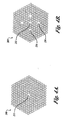
- Resonant cavities are formed from local defect regions within the photonic lattice. Heat can tune the resonant cavities. If the dielectric has been suitably doped with electo-optical polymers, the resonant cavities can be tuned by electric fields suitably adjusting the refractive index of the dielectric. This effect is further discussed in conjunction with FIGURES 4a and 4b below.
- the passive de-multiplexers 112 convey the distinct wavelengths of optical signals into the resonator 140.
- Each resonator is programmed to capture only photons of a programmed wavelength. Other wavelength photons pass through moving from one resonator to the next in a path known as a "shuttle interconnect.”
- the resonators act as small “whispering galleries” by capturing only photons of the programmed wavelength from the inbound light signals. Resonators collect the information the photons carry and then conduct the photons.
- waveguides out of the resonator 140 to the programmed output point at the corresponding digital signal multiplexer 188. Where each of the designated channels for conveying information has a programmed resonator, the incoming signals should be appropriately routed, leaving no remaining ambient light energy.
- the analog beam steering device 160 has a distinct strategy for programmable routing. Rather than resonant cavities, the beam steering device 160 exploits programmable superprisms as "pitchers" and "catchers.” Just as the digital resonator 140 receives the distinct wavelength beams of light at distinct spots from passive de-multiplexers 112, the analog beam steering device 160 similarly receives the beams from the passive de-multiplexers 115. At each of the designated reception ports, an active or semi-active deflector 162 receives the beam. In the analogy to a pitcher, the deflector stands ready to direct the beam at a programmed point.
- the deflector 162 suitably is a photonic crystal or a pair of photonic crystals where at least one crystal is active.
- the pitcher deflector 162 is programmed to aim at one of several "catcher” deflectors 164. Like the pitcher deflector 162 from which it receives the beam, the "catcher” deflector 164 is programmed to appropriately face the "pitcher” reflector 162, and to relay the beam to the programmed analog signal multiplexer 185 corresponding with the programmed output port.
- the pitcher reflectors 162 are programmed as to which catcher deflectors 164 to choose while the catchers deflectors 164 are simultaneously programmed to face the pitcher reflectors 162 and to relay to the multiplexer 185. Because the beams pass one to the other without interference, the signal safely reaches its programmed output multiplexer 185.
- the deflectors, 162 and 164 are suitably superprisms capable of steering beams.
- the simplest means of programming the pitching reflectors 162 and the catching deflectors 164, is to heat the superprism, thereby changing its dimensions. While effective, heating may be less predictable without a cooling airflow. For this reason, electro-optic polymers have been used to programmably steer the beams.
- One of the simplest alternate approaches for using electro-optic organic molecules within photonic crystals includes filling voids in holes that define the photonic crystals. Altering the refractive index of the polymer either optically or electrostatically indirectly tunes the effective cavity length. This effect can be used to modulate an incident light beam. Even more efficient electro-optic switching is expected if the nanocavity design is optimized to include a void at the center of the cavity to place the back-filled electro-optic polymer within the field maximum of the optical standing wave.
- Chip scale steering is enabled by the use of III-V on Silicon, silicon-on-insulator (SOI), and electro-optic polymer technology into compelling wavelength selective devices that enable rapidly reconfigurable wavelength selective routers.
- Devices that in one embodiment may entail III-V gain or electro-optic polymers for use in wavelength selective routers include: (1) electrically pumped photonic crystal micro resonator lasers or gain elements with similar lithographic control and electro-optic polymer tuning; (2) electrically pumped ring or micro disk lasers whose output wavelength is controllable via lithography and potentially tunable through the use of an electro-optic polymer; (3) resonant defect coupled photonic crystal waveguides, also using electo-optic tuning for wavelength routing; and (4) coupling structures that enable the upper layer III-V devices to couple down to the silicon waveguides in the SOI interconnect layer.
- a large bandgap is associated with a triangular superprism 200.
- This geometry is more completely described in the diagram showing the significant dimensions 208.
- the abscissa of the normalized frequency graph includes these dimensions 210. This geometry owes its performance to a high degree of symmetry and will focus light.
- the unique properties of a square geometry differ greatly from a triangular geometry in that there exists a dimension along the diagonal distinct from the lateral dimension.
- the bandgap becomes very narrow.
- the conduction band is very flat. Iso-frequency contours are square allowing the light to collimated. This is the geometry of a photonic crystal resonator. In short, photons of these wavelengths pass through the square lattice. But, light of the appropriate bandgap will collimate, resulting in a photonic crystal resonator.
- a defect 232 is placed in the triangular geometry of a superprism 200 generates similar effects. Rather than the regular repetition of the triangular lattice, the expected hole at 232 is absent, hence the defect. Two effects take over. Total internal reflection and Bragg diffraction, i.e. constructive multiple-beam interference in the periodic structure which can expel light from the material for certain frequencies and directions of incidence are the base phenomenon for photonic crystals.
- a compound semiconductor structure containing an optically active layer is grown on top of the passive ring waveguide as illustrated in FIGURE 5 .
- the evanescent optical field of the ring waveguide overlaps the active layer allowing interaction with the resonant optical mode via photon absorption or emission.
- the amount of loss (or gain) in the resonator, and therefore its Q as well, is then determined by the number of photons coupled into or out of the resonant mode via the active layer.
- External control of the active layer emission is achieved through electrical biasing of a p-n junction (forming a light emitting diode), or by optical pumping at an absorptive wavelength sufficiently removed from the signal channels.
- One presently preferred structure for the micro-resonator 240 is an InGaAsN QW material structure on native substrates (GaAs).
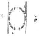
- a cross section of the III-V material structure is shown in FIGURE 6 .
- a perovskite interfacial layer and thin III-V buffer layer are grown directly on the Si surface of the SOI wafer.
- a low refractive index optical isolation layer is grown next, followed by lower carrier confinement layers that sandwich an InGaAsN quantum well active layer.
- the optical isolation layer includes an oxidized high Al mole fraction AlGaAs layer as described below.
- the optical emitting structure may be undoped, if intended for optical pumping, or may contain a doped p-n junction forming an electrically pumped LED structure. In the latter case, an optional etch stop layer may be included within the lower confinement layer to assist in electrical contact formation.
- the refractive index and thickness of layers between the passive Si waveguide 242 and the optically active layer of a III-V stack 244 are important design parameters of the resonator 240 as these factors largely determine the coupling between the two and the strength of the gain/loss control of the resonator 240.
- a high Al mole fraction AlGaAs buffer layer is included above the heteroepitaxial interface layer ( FIGURE 5 ), then laterally oxidized once the resonator structure has been defined by etching.
- the resulting structure of the resonator 240 can be readily produced by current chip formulation techniques as demonstrated in the photomicrograph of FIGURE 6 .
- the same layering forms the waveguides 242 and the stack 244.
Landscapes
- Engineering & Computer Science (AREA)
- Computer Networks & Wireless Communication (AREA)
- Physics & Mathematics (AREA)
- Signal Processing (AREA)
- Chemical & Material Sciences (AREA)
- Optics & Photonics (AREA)
- Nanotechnology (AREA)
- General Physics & Mathematics (AREA)
- Life Sciences & Earth Sciences (AREA)
- Biophysics (AREA)
- Microelectronics & Electronic Packaging (AREA)
- Crystallography & Structural Chemistry (AREA)
- Optical Integrated Circuits (AREA)
- Optical Communication System (AREA)
Claims (16)
- Gemischter analoger und digitaler wellenlängen-selektiver Router im Chipmaßstab, wobei der Router umfasst:einen ersten optischen Demultiplexer (110) der mit einem Eingang einer Faseroptik koppelbar ist, um digitale Signale in einem ersten Wellenlängenbereich von analogen Signalen in einen zweiten Wellenlängenbereich zu trennen;einen zweiten optischen Demultiplexer (112) zum Trennen des ersten Wellenlängenbereichs in eine erste Mehrzahl von Kanälen;einen dritten optischen Demultiplexer (115) zum Trennen des zweiten Wellenlängenbereichs in eine zweite Mehrzahl von Kanälen;eine erste optische Komponente (140), die so eingerichtet ist, dass sie den ersten Wellenlängenbereich empfängt und die erste Mehrzahl von Kanälen programmierbar routet, wobei die erste optische Komponente programmierbare Resonatorfilter umfasst;eine zweite optische Komponente (160), die so eingerichtet ist, dass sie den zweiten Wellenlängenbereich empfängt und die zweite Mehrzahl von Kanälen programmierbar routet, wobei die zweite optische Komponente eine Mehrzahl von Superprismen umfasst; undeine Mehrzahl von optischen Multiplexern (185, 188, 190) die mit der ersten und der zweiten optischen Komponente in optischer Kommunikation stehen.
- Verfahren nach Anspruch 1, wobei die optischen Demultiplexer beabstandete passive optische Elemente umfassen.
- Verfahren nach Anspruch 1, wobei die programmierbaren Resonatorfilter Mikroresonatoren enthalten.
- Verfahren nach Anspruch 3, wobei die Mikroresonatoren Ringe umfassen.
- Verfahren nach Anspruch 3, wobei die Mikroresonatoren Scheiben umfassen.
- Verfahren nach Anspruch 3, wobei die Mikroresonatoren photonische Kristalle umfassen.
- Verfahren nach Anspruch 3, wobei der Mikroresonator durch eine Aktivschicht-Emission gesteuert wird.
- Verfahren nach Anspruch 3, wobei der Mikroresonator durch optisches Pumpen gesteuert wird.
- Verfahren nach Anspruch 3, wobei die Mikroresonatoren in einem Shuttle-Verbindungsverhältnis zueinander gestaltet sind.
- Verfahren zum Routen optischer Signale auf einem Chip, wobei das Verfahren umfasst:Konfigurieren einer ersten optischen Komponente, um ein erstes optisches Signal zu einem ersten optischen Multiplexer entsprechend der Wellenlänge des optischen Signals zu lenken;Konfigurieren einer zweiten optischen Komponente, um ein zweites optisches Signal zu einem zweiten optischen Multiplexer entsprechend der Wellenlänge des optischen Signals zu lenken;Trennen von Licht in analoge Signale in einem ersten Wellenlängenbereich und in digitale Signale in einem zweiten Wellenlängenbereich;Trennen des ersten Wellenlängenbereichs in eine erste Mehrzahl von Kanälen;Trennen des zweiten Wellenlängenbereichs in eine zweite Mehrzahl von Kanälen;Lenken der ersten Mehrzahl von Kanälen zu der ersten optischen Komponente und der zweiten Mehrzahl von Kanälen zu der zweiten optischen Komponente;Routen der an der ersten optischen Komponente empfangenen ersten Mehrzahl von Kanälen zu dem ersten optischen Multiplexer; undRouten der an der zweiten optischen Komponente empfangenen zweiten Mehrzahl von Kanälen zu dem zweiten optischen Multiplexer.
- Verfahren nach Anspruch 10, wobei das Konfigurieren der ersten optischen Komponente ein Konfigurieren steuerbarer Superprismen enthält.
- Verfahren nach Anspruch 11, wobei das Konfigurieren steuerbarer Superprismen ein Heizen des Superprismas auf eine Temperatur entsprechend der zur Temperatur gehörigen Wellenlänge umfasst.
- Verfahren nach Anspruch 11, wobei das Konfigurieren der steuerbaren Superprismen umfasst, dass ein elektro-optisches Polymer einer elektrischen Ladung ausgesetzt wird.
- Verfahren nach Anspruch 10, wobei das Konfigurieren der ersten optischen Komponente ein Konfigurieren photonischer Kristalle umfasst.
- Verfahren nach Anspruch 14, wobei das Konfigurieren photonischer Kristalle umfasst, ein elektro-optisches Polymer einer elektrischen Ladung auszusetzen.
- Verfahren nach Anspruch 14, wobei das Konfigurieren photonischer Kristalle umfasst, ein elektro-optisches organisches Molekül einer elektrischen Ladung auszusetzen.
Applications Claiming Priority (5)
| Application Number | Priority Date | Filing Date | Title |
|---|---|---|---|
| US40407302P | 2002-08-15 | 2002-08-15 | |
| US404073P | 2002-08-15 | ||
| US10/641,334 US7894418B2 (en) | 2002-08-15 | 2003-08-13 | Mixed analog and digital chip-scale reconfigurable WDM network |
| US641334 | 2003-08-13 | ||
| PCT/US2003/025814 WO2004017546A2 (en) | 2002-08-15 | 2003-08-15 | Mixed analog and digital chip-scale reconfigurable wdm network |
Publications (3)
| Publication Number | Publication Date |
|---|---|
| EP1529364A2 EP1529364A2 (de) | 2005-05-11 |
| EP1529364B1 EP1529364B1 (de) | 2008-10-15 |
| EP1529364B2 true EP1529364B2 (de) | 2014-04-02 |
Family
ID=31891420
Family Applications (1)
| Application Number | Title | Priority Date | Filing Date |
|---|---|---|---|
| EP03788605.8A Expired - Lifetime EP1529364B2 (de) | 2002-08-15 | 2003-08-15 | Analog-digital chip-grösse rekonfigurierbares wdm netzwerk |
Country Status (5)
| Country | Link |
|---|---|
| US (2) | US7894418B2 (de) |
| EP (1) | EP1529364B2 (de) |
| AU (1) | AU2003265473A1 (de) |
| DE (1) | DE60324153D1 (de) |
| WO (1) | WO2004017546A2 (de) |
Families Citing this family (15)
| Publication number | Priority date | Publication date | Assignee | Title |
|---|---|---|---|---|
| US7894418B2 (en) * | 2002-08-15 | 2011-02-22 | The Boeing Company | Mixed analog and digital chip-scale reconfigurable WDM network |
| US7539418B1 (en) * | 2005-09-16 | 2009-05-26 | Sun Microsystems, Inc. | Integrated ring modulator array WDM transceiver |
| US9086584B2 (en) * | 2006-08-24 | 2015-07-21 | Cornell University | Dynamic wavelength converter |
| US7961988B2 (en) * | 2006-09-11 | 2011-06-14 | The Boeing Company | Rapidly tunable wavelength selective ring resonator |
| US7609916B2 (en) * | 2007-09-13 | 2009-10-27 | Hewlett-Packard Development Company, L.P. | Electrical contact apparatus for optical waveguides |
| WO2009136913A1 (en) * | 2008-05-06 | 2009-11-12 | Hewlett-Packard Development Company, L.P. | System and method for a micro ring laser |
| US20120257130A1 (en) * | 2011-04-07 | 2012-10-11 | Octrolix Bv | Tunable Wavelength Filter |
| FR2977987B1 (fr) * | 2011-07-11 | 2014-02-14 | Commissariat Energie Atomique | Dispositif laser a cavite en forme de boucle apte a etre fonctinalisee |
| US9164300B2 (en) | 2012-07-02 | 2015-10-20 | Alcatel Lucent | Reconfigurable optical networks |
| EP2940500B1 (de) * | 2014-04-29 | 2025-03-26 | Karlsruher Institut für Technologie | Integrierte optische schaltung und verfahren zu deren herstellung und rekonfiguration |
| US9515733B2 (en) * | 2015-03-05 | 2016-12-06 | Fujitsu Limited | Mitigation of spectral offset in an optical filter |
| US10070208B2 (en) * | 2015-11-30 | 2018-09-04 | Maged E. Beshai | Distributed control of a modular switching system |
| WO2017143160A1 (en) * | 2016-02-18 | 2017-08-24 | Massachusetts Institute Of Technology | Apparatus, systems, and methods for single photon detection |
| US12049580B2 (en) * | 2019-10-15 | 2024-07-30 | Michelle R Stem | Coherent poly propagation materials with 3-dimensional photonic control over visible light |
| TW202614574A (zh) * | 2024-07-31 | 2026-04-01 | 美商天空人工智能股份有限公司 | 使用時脈訊號的數位類比轉換器及包含其的積體電路封裝 |
Family Cites Families (40)
| Publication number | Priority date | Publication date | Assignee | Title |
|---|---|---|---|---|
| US4488307A (en) * | 1982-06-07 | 1984-12-11 | The United States Of America As Represented By The Secretary Of The Navy | Three-mirror active-passive semiconductor laser |
| US5547274A (en) * | 1990-03-14 | 1996-08-20 | Orchard Communications Inc. | Modulated light source with a linear transfer function |
| RU2097815C1 (ru) * | 1993-02-12 | 1997-11-27 | Фирма "Самсунг Электроникс Ко., Лтд." | Оптический процессор |
| JPH09508218A (ja) * | 1994-01-25 | 1997-08-19 | スミス・インダストリーズ・エアロスペイス・アンド・ディフェンス・システムズ、インコーポレイテッド | エレクトロ−オプティカルスイッチを制御する方法及び装置 |
| JPH08316938A (ja) * | 1995-05-17 | 1996-11-29 | Canon Inc | 複数のチャンネルを多重して通信を行う光通信方法及び光通信システム |
| US5926496A (en) | 1995-05-25 | 1999-07-20 | Northwestern University | Semiconductor micro-resonator device |
| CA2273053C (en) * | 1996-12-06 | 2003-01-21 | Bell Communications Research, Inc. | Inter-ring cross-connect for survivable multi-wavelength optical communication networks |
| KR100207602B1 (ko) * | 1996-12-06 | 1999-07-15 | 윤종용 | 광 전력의 손실을 방지하는 광 파장 필터 및 이를 이용한 광 디멀티플렉서 |
| WO1998031184A1 (en) * | 1997-01-07 | 1998-07-16 | Tellium, Inc. | Hybrid wavelength-interchanging cross-connect |
| JP3559680B2 (ja) * | 1997-04-25 | 2004-09-02 | キヤノン株式会社 | リング共振器型面発光半導体レーザ及びその製造法 |
| DE19727706A1 (de) * | 1997-06-30 | 1999-01-07 | Bayer Ag | Thermoplastische Formmassen, ein Verfahren zu deren Herstellung und deren Verwendung sowie ein Verfahren zur Herstellung von Formteilen aus Keramikpulvern |
| US6195187B1 (en) | 1998-07-07 | 2001-02-27 | The United States Of America As Represented By The Secretary Of The Air Force | Wavelength-division multiplexed M×N×M cross-connect switch using active microring resonators |
| BR0008361A (pt) | 1999-02-18 | 2001-11-13 | Siemens Ag | Dispositivo multiplex-add-drop configurável desistema de transmissão-multiplex-comprimento deonda ótico |
| WO2001022141A1 (en) | 1999-09-21 | 2001-03-29 | Nanovation Technologies, Inc. | Wavelength-slicing architecture for wavelength demultiplexing using micro-ring resonators |
| US6636668B1 (en) * | 1999-11-23 | 2003-10-21 | Lnl Technologies, Inc. | Localized thermal tuning of ring resonators |
| JP4161498B2 (ja) * | 1999-12-28 | 2008-10-08 | コニカミノルタホールディングス株式会社 | 光モジュールの製造方法 |
| JP2001203643A (ja) * | 2000-01-21 | 2001-07-27 | Hitachi Ltd | 波長安定化光送信装置 |
| JP2001221041A (ja) | 2000-02-07 | 2001-08-17 | Sanshin Ind Co Ltd | 船外機のマフラ取付構造 |
| US6496616B2 (en) * | 2000-04-28 | 2002-12-17 | Confluent Photonics, Inc. | Miniature monolithic optical demultiplexer |
| JP2001318247A (ja) | 2000-05-08 | 2001-11-16 | Showa Electric Wire & Cable Co Ltd | 3次元フォトニック結晶体及びその製造方法 |
| US6813064B2 (en) * | 2000-07-24 | 2004-11-02 | Sajeev John | Electro-actively tunable photonic bandgap materials |
| DE10036700A1 (de) | 2000-07-27 | 2002-02-14 | Siemens Ag | Modularer optischer Netzwerkknoten |
| AUPQ945500A0 (en) * | 2000-08-15 | 2000-09-07 | Commonwealth Scientific And Industrial Research Organisation | Frequency adjustable oscillator and methods of operation |
| JP4372330B2 (ja) * | 2000-10-30 | 2009-11-25 | 富士通株式会社 | 分布型光増幅装置、光通信用の局および光通信システム |
| US6563627B2 (en) * | 2001-04-06 | 2003-05-13 | Sung-Joo Ben Yoo | Wavelength converter with modulated absorber |
| US6466709B1 (en) * | 2001-05-02 | 2002-10-15 | California Institute Of Technology | Photonic crystal microcavities for strong coupling between an atom and the cavity field and method of fabricating the same |
| US6891993B2 (en) * | 2001-06-11 | 2005-05-10 | The University Of Delaware | Multi-channel wavelength division multiplexing using photonic crystals |
| US7496257B2 (en) * | 2001-07-03 | 2009-02-24 | Brown University Research Foundation | Method and apparatus for detecting multiple optical wavelengths |
| US20030010984A1 (en) | 2001-07-11 | 2003-01-16 | Motorola, Inc. | Integrated light source frequency adjustment, injection locking or modulation of dielectric resonator |
| US6728028B1 (en) * | 2001-07-30 | 2004-04-27 | Cisco Technology, Inc. | Low noise figure optical amplifier for DWDM systems with per sub-band power control |
| US7120338B2 (en) * | 2001-09-10 | 2006-10-10 | California Institute Of Technology | Tuning the index of a waveguide structure |
| US6928091B1 (en) * | 2001-09-26 | 2005-08-09 | Oewaves, Inc. | Opto-electronic oscillator including a tunable electro-optic filter |
| US7116851B2 (en) * | 2001-10-09 | 2006-10-03 | Infinera Corporation | Optical signal receiver, an associated photonic integrated circuit (RxPIC), and method improving performance |
| US20030123827A1 (en) * | 2001-12-28 | 2003-07-03 | Xtalight, Inc. | Systems and methods of manufacturing integrated photonic circuit devices |
| US6853456B2 (en) * | 2002-01-31 | 2005-02-08 | Tip Group, Llc | Method and apparatus for measuring a frequency of an optical signal |
| US7167483B1 (en) * | 2002-05-20 | 2007-01-23 | Ciena Corporation | System and method for managing subrate services in an optical network |
| US6839482B2 (en) * | 2002-06-17 | 2005-01-04 | Lambda Crossing Ltd. | Tunable optical filtering device and method |
| US7894418B2 (en) * | 2002-08-15 | 2011-02-22 | The Boeing Company | Mixed analog and digital chip-scale reconfigurable WDM network |
| JP3830962B2 (ja) * | 2004-05-20 | 2006-10-11 | 松下電器産業株式会社 | フォトニック結晶デバイス |
| US7869470B2 (en) * | 2005-08-31 | 2011-01-11 | The Trustees Of Columbia University In The City Of New York | Devices and methods for providing stimulated raman lasing |
-
2003
- 2003-08-13 US US10/641,334 patent/US7894418B2/en active Active
- 2003-08-15 DE DE60324153T patent/DE60324153D1/de not_active Expired - Lifetime
- 2003-08-15 AU AU2003265473A patent/AU2003265473A1/en not_active Abandoned
- 2003-08-15 EP EP03788605.8A patent/EP1529364B2/de not_active Expired - Lifetime
- 2003-08-15 WO PCT/US2003/025814 patent/WO2004017546A2/en not_active Ceased
-
2011
- 2011-02-20 US US13/031,227 patent/US10425706B2/en not_active Expired - Fee Related
Also Published As
| Publication number | Publication date |
|---|---|
| US7894418B2 (en) | 2011-02-22 |
| WO2004017546A3 (en) | 2004-09-16 |
| US20040114930A1 (en) | 2004-06-17 |
| US10425706B2 (en) | 2019-09-24 |
| WO2004017546A2 (en) | 2004-02-26 |
| EP1529364A2 (de) | 2005-05-11 |
| DE60324153D1 (de) | 2008-11-27 |
| EP1529364B1 (de) | 2008-10-15 |
| AU2003265473A1 (en) | 2004-03-03 |
| US20120251107A1 (en) | 2012-10-04 |
Similar Documents
| Publication | Publication Date | Title |
|---|---|---|
| US10425706B2 (en) | WDM router | |
| CN100574023C (zh) | 可调谐激光器 | |
| EP2252906B1 (de) | Optoelektronische schalter mit optischen wellenleitern auf dem chip | |
| US6618535B1 (en) | Photonic bandgap device using coupled defects | |
| Grover et al. | Parallel-cascaded semiconductor microring resonators for high-order and wide-FSR filters | |
| US8331743B2 (en) | Reconfigurable optical filters formed by integration of electrically tunable microresonators | |
| KR101443728B1 (ko) | 하이브리드 도파-모드 공진 필터 및 분포 브래그 반사를 채용하는 방법 | |
| US7961988B2 (en) | Rapidly tunable wavelength selective ring resonator | |
| US20180348507A1 (en) | Wavelength tunable optical sources, filters and detectors | |
| EP1506442A2 (de) | Fotonenkristallvorrichtung | |
| US10962716B2 (en) | Microelectromechanically actuated deformable optical beam steering for wavelength tunable optical sources, filters, and detectors | |
| WO2002019000A1 (en) | Microcavity-based optical channel router | |
| CN105452950A (zh) | 光信号处理装置 | |
| US6934436B2 (en) | Thermo-optical switch using coated microsphere resonators | |
| Haldar et al. | Theory and design of off-axis microring resonators for high-density on-chip photonic applications | |
| Prabha et al. | Two-dimensional photonic crystal-based filters review | |
| US6917744B2 (en) | Optical multiplexing and demultiplexing device, optical communication apparatus, and optical communication system | |
| Sridarshini et al. | Photonic crystal based routers for all optical communication networks | |
| US20250306284A1 (en) | Methods and systems for optical transmitters exploiting multiple gain elements | |
| Dideban et al. | Photonic crystal channel drop filters based on circular-shaped cavities | |
| US8005328B2 (en) | Optical add/drop module | |
| SE526498C2 (sv) | Anordning för optisk koppling samt array, förfarande och användning | |
| US11675134B1 (en) | Optical bandpass filter based on reflective devices | |
| Yang et al. | 2× 3 Photonic crystal series-parallel integrated sensor arrays based on monolithic substrates using side-coupled resonator arrays | |
| WO2026073342A1 (en) | Optical systems exploiting remote sources, coherent photonic interposer circuits and electronic-photonic integrated circuits |
Legal Events
| Date | Code | Title | Description |
|---|---|---|---|
| PUAI | Public reference made under article 153(3) epc to a published international application that has entered the european phase |
Free format text: ORIGINAL CODE: 0009012 |
|
| 17P | Request for examination filed |
Effective date: 20050307 |
|
| AK | Designated contracting states |
Kind code of ref document: A2 Designated state(s): AT BE BG CH CY CZ DE DK EE ES FI FR GB GR HU IE IT LI LU MC NL PT RO SE SI SK TR |
|
| AX | Request for extension of the european patent |
Extension state: AL LT LV MK |
|
| DAX | Request for extension of the european patent (deleted) | ||
| RBV | Designated contracting states (corrected) |
Designated state(s): DE FR |
|
| GRAP | Despatch of communication of intention to grant a patent |
Free format text: ORIGINAL CODE: EPIDOSNIGR1 |
|
| GRAS | Grant fee paid |
Free format text: ORIGINAL CODE: EPIDOSNIGR3 |
|
| GRAA | (expected) grant |
Free format text: ORIGINAL CODE: 0009210 |
|
| AK | Designated contracting states |
Kind code of ref document: B1 Designated state(s): DE FR |
|
| REF | Corresponds to: |
Ref document number: 60324153 Country of ref document: DE Date of ref document: 20081127 Kind code of ref document: P |
|
| PLBI | Opposition filed |
Free format text: ORIGINAL CODE: 0009260 |
|
| PLAX | Notice of opposition and request to file observation + time limit sent |
Free format text: ORIGINAL CODE: EPIDOSNOBS2 |
|
| 26 | Opposition filed |
Opponent name: AIRBUS SAS(FR)/ AIRBUS OPERATIONS SAS(FR)/ AIRBUS Effective date: 20090713 |
|
| PLAF | Information modified related to communication of a notice of opposition and request to file observations + time limit |
Free format text: ORIGINAL CODE: EPIDOSCOBS2 |
|
| PLBB | Reply of patent proprietor to notice(s) of opposition received |
Free format text: ORIGINAL CODE: EPIDOSNOBS3 |
|
| REG | Reference to a national code |
Ref country code: DE Ref legal event code: R082 Ref document number: 60324153 Country of ref document: DE |
|
| PUAH | Patent maintained in amended form |
Free format text: ORIGINAL CODE: 0009272 |
|
| STAA | Information on the status of an ep patent application or granted ep patent |
Free format text: STATUS: PATENT MAINTAINED AS AMENDED |
|
| 27A | Patent maintained in amended form |
Effective date: 20140402 |
|
| AK | Designated contracting states |
Kind code of ref document: B2 Designated state(s): DE FR |
|
| REG | Reference to a national code |
Ref country code: DE Ref legal event code: R102 Ref document number: 60324153 Country of ref document: DE |
|
| REG | Reference to a national code |
Ref country code: DE Ref legal event code: R102 Ref document number: 60324153 Country of ref document: DE Effective date: 20140402 |
|
| REG | Reference to a national code |
Ref country code: FR Ref legal event code: PLFP Year of fee payment: 14 |
|
| REG | Reference to a national code |
Ref country code: FR Ref legal event code: PLFP Year of fee payment: 15 |
|
| REG | Reference to a national code |
Ref country code: FR Ref legal event code: PLFP Year of fee payment: 16 |
|
| PGFP | Annual fee paid to national office [announced via postgrant information from national office to epo] |
Ref country code: DE Payment date: 20220829 Year of fee payment: 20 |
|
| PGFP | Annual fee paid to national office [announced via postgrant information from national office to epo] |
Ref country code: FR Payment date: 20220825 Year of fee payment: 20 |
|
| REG | Reference to a national code |
Ref country code: DE Ref legal event code: R071 Ref document number: 60324153 Country of ref document: DE |