EP1528667A2 - Amplificateur variable et terminal mobile sans fil comprenant un tel amplificateur - Google Patents
Amplificateur variable et terminal mobile sans fil comprenant un tel amplificateur Download PDFInfo
- Publication number
- EP1528667A2 EP1528667A2 EP04025774A EP04025774A EP1528667A2 EP 1528667 A2 EP1528667 A2 EP 1528667A2 EP 04025774 A EP04025774 A EP 04025774A EP 04025774 A EP04025774 A EP 04025774A EP 1528667 A2 EP1528667 A2 EP 1528667A2
- Authority
- EP
- European Patent Office
- Prior art keywords
- transistors
- base
- variable amplifier
- signal
- amplifier
- Prior art date
- Legal status (The legal status is an assumption and is not a legal conclusion. Google has not performed a legal analysis and makes no representation as to the accuracy of the status listed.)
- Granted
Links
Images






Classifications
-
- H—ELECTRICITY
- H03—ELECTRONIC CIRCUITRY
- H03G—CONTROL OF AMPLIFICATION
- H03G1/00—Details of arrangements for controlling amplification
- H03G1/0005—Circuits characterised by the type of controlling devices operated by a controlling current or voltage signal
- H03G1/0035—Circuits characterised by the type of controlling devices operated by a controlling current or voltage signal using continuously variable impedance elements
- H03G1/007—Circuits characterised by the type of controlling devices operated by a controlling current or voltage signal using continuously variable impedance elements using field-effect transistors [FET]
-
- H—ELECTRICITY
- H03—ELECTRONIC CIRCUITRY
- H03F—AMPLIFIERS
- H03F1/00—Details of amplifiers with only discharge tubes, only semiconductor devices or only unspecified devices as amplifying elements
- H03F1/08—Modifications of amplifiers to reduce detrimental influences of internal impedances of amplifying elements
- H03F1/22—Modifications of amplifiers to reduce detrimental influences of internal impedances of amplifying elements by use of cascode coupling, i.e. earthed cathode or emitter stage followed by earthed grid or base stage respectively
-
- H—ELECTRICITY
- H03—ELECTRONIC CIRCUITRY
- H03F—AMPLIFIERS
- H03F1/00—Details of amplifiers with only discharge tubes, only semiconductor devices or only unspecified devices as amplifying elements
- H03F1/30—Modifications of amplifiers to reduce influence of variations of temperature or supply voltage or other physical parameters
- H03F1/302—Modifications of amplifiers to reduce influence of variations of temperature or supply voltage or other physical parameters in bipolar transistor amplifiers
-
- H—ELECTRICITY
- H03—ELECTRONIC CIRCUITRY
- H03G—CONTROL OF AMPLIFICATION
- H03G1/00—Details of arrangements for controlling amplification
- H03G1/0005—Circuits characterised by the type of controlling devices operated by a controlling current or voltage signal
- H03G1/0035—Circuits characterised by the type of controlling devices operated by a controlling current or voltage signal using continuously variable impedance elements
- H03G1/0082—Circuits characterised by the type of controlling devices operated by a controlling current or voltage signal using continuously variable impedance elements using bipolar transistor-type devices
Definitions
- the present invention relates to variable amplifiers offering variable overall characteristics including gain, linearity, and noise performance and relates also to mobile wireless terminals using such an amplifier with received signals.
- Mobile wireless terminals need to adopt to variable reception power and adjust transmission power. To address these needs, many variable gain amplifiers are used to vary gain.
- variable gain amplifiers in receiver circuitry are required to reduce noise to a minimum and provide a large gain when the reception power is low. At high reception powers, they are required, among other things, to provide high linearity in order to prevent the high input power from distorting the output.
- variable gain amplifier filling these requirements is disclosed in "A Low-Noise Wideband Variable-Gain Amplifier Using an Interpolated Ladder Attenuator," ISSCC Digest of Technical Papers, pp. 280-281, Feb. 1991 (“ISSCC Digest”) and Technical Report of Signal Science, Vol. 96, No. 462, ED 96-198, pp. 9-14, 1997 (“Technical Report”).
- the variable gain amplifier achieves low noise at large gains and high linearity at small gains through a combined use of a set of amplifiers with identical characteristics and multiple stages of attenuators.
- variable gain amplifier in mobile wireless terminal receiver circuitry is required to achieve a wide variation range, low noise, and high linearity.
- Differential circuitry may be used in a variable gain amplifier to attain these goals.
- variable gain amplifier is disclosed in Japanese unexamined patent application 2002-252532 ("Tokukai 2002-252532"; published on September 6, 2002).
- the amplifier contains an input section and an output section.
- the input section contains a set of variable gain amplifier circuits, each exhibiting a decreasing gain with an increase in an external control voltage, connected in parallel.
- the emitters of the first and second transistors are connected to a constant current source and connected also to each other through an intervening emitter resistor.
- the first and second transistors output collector currents via their collectors. Receiving the collector current inputs from the input section, the output section produces output signals at a gain in accordance with the control voltage for output.
- variable gain amplifiers disclosed in the ISSCC Digest, the Technical Report, and Tokukai 2002-252532 are designed to operate on a differential input signal. They cannot be directly connected to a signal source of single-ended (unbalanced) signals.
- the antenna which is the signal source for the variable gain amplifier, outputs single-ended signals.
- balun when building a conventional variable gain amplifier into receiver circuitry, it is essential to provide a balun to convert the single-ended signal output from the antenna to a differential signal.
- the balun is difficult to fabricate in an integrated circuit by silicon processing, which in turn gives trouble in integrating the entire receiver circuitry into a single integrated circuit when using the conventional variable gain amplifier along with the receiver circuitry.
- the balun If the balun is to be used with receiver circuitry, but built separately from the integrated circuit as a chip component, the receiver circuitry will need an increased footprint and thickness in mounting. In addition, if the balun is used with the receiver circuitry, the balun dissipates some of the reception power, degrading reception sensitivity and other quality factors.
- the present invention has an objective to provide a variable amplifier which can be directly connected to an antenna, filter coupled with it, or other single-ended signal source, with no intervening balun or like components, and provide also a mobile wireless terminal containing receiver circuitry which requires reduced mounting footprint and thickness, but boasts excellent reception sensitivity and other characteristics.
- a variable amplifier of the present invention includes multiple parallel signal-amplifying bipolar transistors between a signal input terminal and a signal output terminal.
- the emitters of the transistors are substantially grounded.
- At least one of the paths extending from the signal input terminal to the signal output terminal through the transistors differs from the other paths in a characteristic (signal amplifying gain, linearity, noise performance, etc.).
- the variable amplifier has a feature that it contains a base current control section controlling the base currents of the transistors so that the variable amplifier exhibits a variable overall characteristic.
- the variable amplifier is not differential, but in a simple common emitter configuration. Therefore, the input is single-ended.
- the variable amplifier When connected to a single-ended signal source, such as an antenna or a filter connected to the antenna, the variable amplifier needs no balun or like single-ended/differential converter.
- the variable amplifier therefore can be directly coupled to a single-ended signal source.
- the variable amplifier exhibits a desirable range of variable gain, linearity, noise, and other characteristics.
- the base current control section preferably controls the base currents of the transistors so as to vary the overall gain of the variable amplifier.
- a variable gain amplifier is realized.
- the paths preferably include first signal paths and a second signal path which amplifies a signal at a smaller signal amplifying gain and higher signal amplifying linearity than the first signal paths.
- the second signal path preferably has an attenuator attenuating a signal between the associated one of the transistors and the input terminal.
- variable amplifier of the present invention may be adapted so that the collectors of the transistors are substantially connected to a single load.
- variable amplifier of the present invention may further include a secondary transistor with its emitter or source substantially connected to the collectors of the transistors.
- the base or gate of the secondary transistor is grounded in terms of high frequency components and the collector or drain of the secondary transistor is substantially connected to a load.
- the transistors are substantially cascaded to the secondary transistor.
- the variable amplifier is thus capable of easing mirror effect and improves the range of variable gain and linearity.
- the "grounding in terms of high frequency components” refers to the connection to a voltage source of a sufficiently low impedance at operating frequency.
- the base needs to be coupled to a constant voltage. It was therefore desirable to provide a voltage source (voltage generate circuit) generating the constant voltage for connection to the bases of the common base circuit.
- a simple method to generate a desired voltage is to divide a source voltage. This requires sufficiently low impedance, which can be achieved by, for example, passing five times as much current through the voltage divider resistors as through the base current of the common base circuit or coupling a capacitor to the base of the common base circuit for sufficiently low impedance at operating frequency.
- variable amplifier of the present invention may include multiple secondary transistors each having an emitter or a source connected to a different one of the collectors of the transistors.
- the arrangement prevents signal leak from non-operating common emitter transistors, thereby achieving high signal isolation. This extends the range of variable gain and improves linearity.
- variable amplifier of the present invention may further include a voltage control section controlling base voltages or gate voltages of the secondary transistors.
- the base voltages or gate voltages of the secondary transistors can be actively turned off in accordance with the operation status of the common emitter transistors. This further improves the characteristics.
- variable amplifier of the present invention may be adapted so that the voltage control section allows substantially zero base voltages or gate voltages for the secondary transistors when the base currents of the transistors are below or equal to a predetermined level.
- the arrangement eases the development of distortion in the common emitter transistors when the base currents of the transistors are near zero (turned off).
- variable amplifier of the present invention may be adapted so that the transistors form respective unit amplifiers, and at least one of the unit amplifiers differs from other unit amplifiers in a characteristic.
- the arrangement optimizes the characteristics of the unit amplifiers in accordance with the characteristics required with the individual unit amplifiers, thus greatly improving overall characteristics of the variable amplifier.
- the paths include first signal paths and a second signal path which amplifies a signal at a smaller gain than the first signal paths, and the unit amplifier on the second signal path has higher linearity than the unit amplifiers on the first signal paths.
- Higher linearity can be given to the unit amplifier on the second signal path than to the unit amplifiers on the first signal paths by, for example, the following techniques: (1) Negative feedback is given to the transistor forming the unit amplifier on the second signal path, whereas no negative feedback is given to the transistors forming the unit amplifiers on the first signal paths. (2) Current density is increased by designing the transistor forming the unit amplifier on the second signal path in smaller size than transistors forming the unit amplifiers on the first signal paths.
- variable amplifier of the present invention may be adapted so that the base current control section controls the base currents of the transistors so that a combined current consumption in the transistors varies in accordance with a change in a ratio of the base currents of the transistors.
- the arrangement enables regulation of the current consumption in the transistors in accordance with the characteristics needed by the unit amplifiers formed by the transistors. This eliminates the overall current consumption in the variable amplifier.
- a mobile wireless terminal of the present invention is characterized in that it includes an amplifier amplifying a received signal and the amplifier is the variable amplifier having one of the foregoing arrangements.
- the arrangement enables direct coupling of the input of the variable amplifier to an antenna or a bandpass filter directly coupled to the antenna.
- a balun is thus no longer required which would be necessary in mobile wireless terminals built around a conventional, differential variable gain amplifier circuit.
- the elimination of the balun not only contributes to the overall circuit downsizing in the mobile wireless terminal, but also to reception power savings by eliminating the power dissipation in the balun. This realizes more compact, high performance (high sensitivity) mobile wireless terminals with an extended operation time.
- variable amplifier of the present embodiment is arranged to vary its overall gain and linearity by switching between a set of unit amplifiers connected in parallel between a signal input and a signal output.
- the switchable stage count i.e., the number of switchable unit amplifiers
- the count is 3 in the Figure 1 example (detailed description will be given later).
- variable amplifier of the present embodiment at least one of the signal paths which extend from the signal input to the signal output via a set of transistors differs in gain and linearity from the others, so that the overall gain and linearity of the variable amplifier can vary with the switching between the unit amplifiers.
- each signal path from the signal input to one of the transistors differs in attenuation from the others.
- each unit amplifier contains only one transistor, i.e. one stage, which is an npn bipolar transistor. Further, all the transistors have the same characteristics: specifically, they are all SiGe bipolar transistors with an 20 _m ⁇ 0.5 _m emitter area.
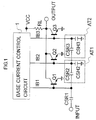
- Figure 1 is a circuit diagram illustrating the arrangement of a variable amplifier in accordance with an embodiment of the present invention (the base current control circuit is represented by a block).
- the variable amplifier of the present embodiment contains three signal-amplifying transistors: a first transistor Q1, a second transistor Q2, and a third transistor Q3 (detailed later).
- the amplifier also contains a base current control circuit (base current control section or base current switching circuit) 1.
- the transistors Q1 to Q3 are connected in parallel between an input terminal (signal input terminal) INPUT where a signal having a DC component is applied and an output terminal (signal output terminal) OUTPUT where the signal is output after being amplified.
- the transistors Q1 to Q3 are grounded at their emitters.
- the collectors of the transistors Q1 to Q3 are connected to the output terminal OUTPUT and also to the same end of a common load resistor RL.
- the other end of the resistor RL is connected to a power supply line VCC through which is supplied a source voltage.
- the input terminal INPUT is connected to the base of the first transistor Q1 via a capacitor CSR1 which removes the DC component from the input signal.
- the input terminal INPUT is connected also to the base of the second transistor Q2 via the capacitor CSR1 and an attenuator AT1 which attenuates an input signal.
- the attenuator AT1 contains a capacitor CSR2 and capacitor CSH2.
- the capacitor CSR2 is connected in series with the base of the first transistor Q1 and in series with the capacitor CSR1.
- the capacitor CSH2 shunts a signal path successive to the capacitor CSR2, i.e. a signal path connecting the capacitor CSR2 to the base of the second transistor Q2, to ground.
- the input terminal INPUT is connected to the base of the third transistor Q3 via the capacitor CSR1, the attenuator AT1, and another attenuator AT2 which attenuates the input signal.
- the attenuator AT2 contains a capacitor CSR3 and a capacitor CSH3.
- the capacitor CSR3 is connected in series with the base of the second transistor Q2 and in series with the capacitor CSR2.
- the capacitor CSH3 shunts a signal path successive to the capacitor CSR3, i.e. a signal path connecting the capacitor CSR3 to the base of the third transistor Q3, to ground.
- the transistor Q1 receives a signal fed to the input terminal INPUT directly, i.e. without no intervening attenuator.
- the Q1 path is therefore has the largest gain of the three signal paths.
- the transistor Q2 receives a signal fed to the input terminal INPUT via the attenuator AT1.
- the Q2 path therefore has a smaller gain and higher linearity than the Q1 path.
- the transistor Q3 receives a signal fed to the input terminal INPUT via the attenuators AT1, AT2.
- the Q3 path therefore has a smaller gain and higher linearity than the Q2 path.
- the bases of the transistors Q1 to Q3 are connected to the terminals IB1 to IB3 of the base current control circuit 1 so that the base current control circuit 1 can control the individual current flows through the bases of the transistors Q1 to Q3 (base currents).
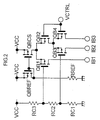
- the base current control circuit 1 contains: resistors RC1, RC2, RC3 producing reference voltages; a resistor RREF setting a base current sum; field effect transistors QBREF, QBCS constituting a current mirror circuit which sets a current sum; field effect transistors QB1, QB2 constituting a first differential pair; and field effect transistors QB3, QB4 constituting a second differential pair.
- the transistors QBREF, QBCS, QB1, QB2, QB3, QB4 are p-channel MOS (metal oxide semiconductor) transistors.
- the transistors QBREF, QBCS constitute a current mirror circuit: the gate and drain of the transistor QBREF and the gate of the transistor QBCS are all connected together.
- the transistor QBREF is coupled to the power supply line VCC at its source and to an end of the resistor RREF at its drain and gate. The other end of the resistor RREF is grounded.
- the transistor QBCS is coupled to the power supply line VCC at its source and to the sources of the transistors QB1, QB2 at its drain.
- the current mirror circuit sets the sum of the current flows through the bases of the transistors Q1 to Q3 (hereinafter, the "base current sum") so that the sources of the transistors QB1, QB2 conduct a combined current flow which is equal to the current sum setting.
- the current setting resistor RREF dictates the current flow through the gate and drain of the transistor QBREF. Based on this current flow, the current mirror circuit determines the current flow through the sources of the transistors QB1, QB2 (base current sum). If the transistor QBREF and the transistor QBCS, combined to form a current mirror circuit, are of the same size, the combined current flow through the drains of the transistors QB1, QB2 (base current sum) becomes equal to the current determined by the current setting resistor RREF which is invariable over time.
- the resistors RC1, RC2, RC3 are connected in series between the power supply line VCC through which is supplied a source voltage and ground. They divide the source voltage to produce reference voltages VR1, VR2 (VR1 ⁇ VR2).
- the transistors QB1, QB2 are coupled to each other at their sources, thus forming the first differential pair.
- the gate of the transistor QB1 is fed with the reference voltage VR2. Meanwhile, the gate of the transistor QB2 is fed with an external variable control voltage VCTRL via a control voltage terminal VCTRL.
- the drain of the transistor QB1 is coupled to the base of the transistor Q1 via the terminal IB1.
- the drain of the transistor QB2 is coupled to the sources of the transistors QB3, QB4.
- the first differential pair determines a ratio of the current flow through the base of the transistor Q1 and the current flow through the sources of the transistors QB3, QB4 in accordance with the magnitude relationship between the control voltage VCTRL and the reference voltage VR2.
- the transistors QB3, QB4 are coupled to each other at their sources, thus forming the second differential pair.
- the gate of the transistor QB3 is fed with the reference voltage VR1.
- the gate of the transistor QB4 is fed with an external variable control voltage VCTRL via a control voltage terminal VCTRL.
- the drain of the transistor QB3 is coupled to the base of the transistor Q2 via the terminal IB2.
- the drain of the transistor QB4 is coupled to the base of the transistor Q3 via the terminal IB3.
- the second differential pair determines a ratio of the current flow through the base of the transistor Q2 and the current flow through the base of the transistor Q3 in accordance with the magnitude relationship between the control voltage VCTRL and the reference voltage VR1.
- the base current sum flowing through the sources of the transistors QB1, QB2 at a value determined by the transistors QBREF, QBCS are divided among the terminals IB1 to IB3 by means of the transistors QB1, QB2, QB3, QB4 in accordance with the control voltage VCTRL.
- the ratio of current values IB1 to IB3 at the terminals IB1 to IB3 (that is, at the bases of the transistors Q1 to Q3) changes continuously in accordance with the control voltage VCTRL.
- Figure 3 illustrating the switching characteristics of the current flows through the bases of the transistors Q1 to Q3 (base currents), that is, changes in the base currents with the control voltage.
- the proportion of the current value IB1 to the base current sum stays at 0% when the control voltage VCTRL is up to about 0.9 V and continuously increases from 0% to 100% when the control voltage VCTRL rises from the about 0.9 V to about 2.35 V.
- the proportion is 100% when the control voltage VCTRL is in excess of about 2.35 V.
- the proportion of the current value IB2 to the base current sum stays at 0% when the control voltage VCTRL is up to about 0.2 V and continuously increases from 0% to about 80% when the control voltage VCTRL rises from about 0.2 V to about 1.35 V.
- the proportion of the current value IB3 to base current sum is 100% when the control voltage VCTRL less than about 0.2 V and continuously decreases from 100% to 0% when the control voltage VCTRL rises from about 0.2 V to about 1.45 V.
- the proportion stays at 0% when the control voltage VCTRL is in excess of about 1.45 V.
- the transistors QB2, QB4 in the base current control circuit 1 turn off. This causes the base current sum, as determined by the current mirror circuit (transistors QBREF, QBCS) used for current sum setting purposes, to entirely flow to the base of the transistor Q1 in the amplifier via the transistor QB1.
- the other transistors Q2, Q3 turn off.
- the transistor Q1 receives the signal fed to the input terminal INPUT with no intervening attenuators, producing the greatest gain.
- IIP3 Input third order Intercept Point or third order intermodulation expressed in dB_V or dBc
- the control voltage VCTRL falls, the current flow through the base of the transistor Q1 is partially diverted to the base of the transistor Q2. Specifically, with a falling control voltage VCTRL, the base current of the transistor Q1 gradually decreases, and the base current of the transistor Q2 gradually increases. In the transistor Q1, the collector current thus decreases, gradually reducing the gain. In contrast, in the transistor Q2, the collector current increases, gradually raising the gain. Since the Q2 path has a lower gain than the Q1 path at the same base current as mentioned earlier, the overall gain of the variable amplifier drops (see Figure 4). Moreover, since the Q2 path has high linearity than the Q1 path at the same base current as mentioned earlier, the overall linearity of the variable amplifier rises (see Figure 4).
- variable amplifier exhibits a relatively small overall gain due to the presence of the attenuator AT1 on the input path of the transistor Q2.
- IIP3 of the variable amplifier as a whole is equivalent to the property of the transistor Q2 plus the attenuation ratio in decibels (dB).
- the transistors QB1, QB3 turn off.
- all of the base current sum as determined by the resistor RREF and the transistors QBREF, QBCS in the base current control circuit 1 flows to the base of the transistor Q3 via the transistor QB1, turning off both the other transistors Q1, Q2.
- the signal fed to the input terminal INPUT is supplied to the transistor Q3 via the attenuators AT1, AT2.
- the variable amplifier exhibits the lowest overall gain. Conversely, IIP3 of the variable amplifier as a whole is highest.
- variable amplifier of the present embodiment offers variable gain over a wide range and achieves high linearity at a large-signal, low-gain condition.
- the variable amplifier of the present embodiment contains amplifier circuitry of a common emitter configuration, not a differential circuit configuration which is often used in silicon RFICs (radio frequency integrated circuits). Therefore, the variable amplifier of the present embodiment receives a single-ended signal input (unbalanced input), not a differential signal input. This enables the variable amplifier of the present embodiment to be directly connected to an antenna, filter, and other single-ended signal sources.
- variable amplifier of the present embodiment therefore operates at low source voltages: for example, as low as about 1 V.
- the differential circuit needs a current source, an amplifier section, and a load resistor.
- the amplifier section needs be made up of two stages of transistors, and the source voltage cannot be reduced much.
- the gain-control voltage characteristic of the variable amplifier shown in Figure 1 contains small curves and is not much linear.
- the gain-control voltage characteristic however becomes more linear with a greater switchable stage count (number of switchable unit amplifiers), at a cost of increased circuit dimensions.
- the switchable stage count should hence be determined so as to strike a good balance between the circuit dimensions and the linearity of the gain-control voltage characteristic.
- the present embodiment so far having assumed an npn transistor, may be applied to a pnp transistor to provide a similar variable amplifier.
- the present embodiment has so far assumed the attenuators AT1, AT2, inserted between the input terminal INPUT and the transistors Q2, Q3, being built around a capacitor.
- the capacitor-based attenuator structure is by no means limited in any particular manner. Other structures are also available.
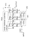
- the capacitor-based attenuators AT1, AT2 may both be replaced with resistor-based attenuators AT3, AT4. In such cases, however, the bases of the transistors Q1 to Q3 need be DC-isolated from the attenuators AT3, AT4 for operation. This is done by inserting capacitors CDC1, CDC2, CDC3 respectively between the transistors Q1 to Q3 in a common emitter configuration and the attenuators AT3, AT4.
- a resistor RSR1 is provided between the bases of the transistors Q1 to Q3 and the input terminal INPUT.
- the attenuator AT3 contains a resistor RSR2 and a resistor RSH2.
- the resistor RSR2 is connected in series with the base of the first transistor Q1 and in series with the resistor RSR1.
- the resistor RSH2 shunts a signal path successive to the resistor RSR2, i.e. a signal path connecting the resistor RSR2 to the base of the second transistor Q2, to ground.
- the attenuator AT4 contains a resistor RSR3 and a resistor RSH3.
- the resistor RSR3 is connected in series with the base of the second transistor Q2 and in series with the resistor RSR2.
- the resistor RSH3 shunts a signal path successive to the resistor RSR3, i.e. a signal path connecting the resistor RSR3 to the base of the third transistor Q3, to ground.
- the resistor-based attenuators AT3, AT4 have following advantages over the capacitor-based attenuators: (1) They make the variable amplifier smaller and especially, when integrated into a chip, occupy a smaller chip area. (2) They permit less signal leak in the variable amplifier and especially, when the circuitry is mounted on a single board, less signal leak through the board. (3) They are more readily matched.
- the resistor-based attenuator structure is again by no means limited in any particular manner. Also, in the structure in Figure 5, the resistor RSR1 is not essential.
- the base current control circuit is the analog circuit arranged as shown in Figure 2.
- this base current control circuit for use with base current is not limited in any particular manner provided that it is capable of continuously changing the ratio of current values IB1 to IB3 at the bases of the transistors Q1 to Q3 over a predetermined range in accordance with the control voltage VCTRL.
- the base current control circuit may be structured to digitally control the base currents of the transistors Q1 to Q3 by using a D/A (digital-analog) converter. Base current control circuits of different structures may also be used when the base currents of the transistors Q1 to Q3 is controlled by means of analog circuitry.
- the base current control circuit of the present embodiment is designed to produce a substantially constant base current sum.
- the base current sum is not necessarily constant. A large current may be supplied to an amplifier section where linearity matters, and a small current to an amplifier section where linearity does not matter much.
- the base current sum may be greater when producing a maximum base current for the transistor Q3 where linearity matters in comparison with the other transistors Q1, Q2 than when producing a maximum base current for the transistor Q2.
- the base current sum may be smaller when producing a maximum base current for the transistor Q1 where linearity does not matter much than when producing a maximum base current for the transistor Q2.
- the base currents of the transistors Q2, Q3 may be reduced while providing such a negative feedback to the transistors Q2, Q3 that results in sufficient linearity.
- the transistor Q1 needs some current because it needs to offer all the high linearity, low noise, and large gain performance.
- the transistors Q2, Q3 meanwhile are not required to offer that level of high gain, low noise performance, allowing the use of a negative feedback to reduce power consumption. Note an advantage of a constant base current sum for the transistors Q1 to Q3: the DC voltage output becomes substantially constant.
- variable amplifier of the present embodiment has so far assumed that each signal path extending from the signal input terminal to the signal output terminal via a set of transistors has different characteristics from the others. However, some of the signal paths may share the same characteristics provided that at least one of them has different characteristics from the others.
- variable amplifier of the present embodiment has so far assumed that its gain and linearity are changeable through the control of the current flow through the bases of the transistors. Alternatively, any other characteristics may be changeable through the control of the current flow through the bases of the transistors.
- variable amplifier of the present embodiment contains a set of bipolar transistors having their emitters substantially grounded and collectors connected to substantially identical loads.
- the amplifier changes its overall characteristics through changes of the base currents through the transistors.
- This structure employs a simple common emitter configuration, not a differential circuit.
- the input is single ended, and no single-ended or differential converter, such as a balun, is needed.
- the amplifier offers desirable characteristics, including a range of variable gain, linearity, and noise performance.
- variable amplifier of the present embodiment is an amplifier circuit with a set of emitters being grounded.
- the variable amplifier achieves a wide range of gains and linearity by changing its overall characteristics through continuous (analog) switching by means of an analog signal between the base currents of the bipolar transistors used in the amplification.
- variable amplifier of embodiment 1 the base/collector capacitances of the transistors Q1 to Q3 are increased by mirror effect due to the simple common emitter configuration.
- the variable amplifier of embodiment 1 does not therefore exhibit very good characteristics at high frequencies.
- variable amplifier of the present embodiment employs a cascade connection to improve characteristics at high frequencies.
- Figure 6 illustrates the arrangement of a variable amplifier of the present embodiment.
- the collectors of the common emitter transistors Q1 to Q3 were connected to a load resistor RL.
- the common emitter bipolar transistors Q1 to Q3 are cascaded to a secondary transistor Q4.
- the emitter of the transistor Q4 is coupled to the collectors of the common emitter transistors Q1 to Q3.
- the collector of the transistor Q4 is coupled to the load resistor RL.
- VBB a fixed bias voltage
- a transistor which is grounded in terms of high frequency components like this one will be referred to as a "common base transistor.” This is the only major difference between the arrangement of the variable amplifier of embodiment 1 and that of the variable amplifier of the present embodiment.
- variable amplifier of the present embodiment contains npn bipolar transistors as the common emitter transistors Q1 to Q3.
- the common base transistor Q4 is also an npn bipolar transistor.
- the base currents of the common emitter transistors Q1 to Q3 are under the control of the base current control circuit 1 shown in the circuit diagram of Figure 2.
- the variable amplifier of the present embodiment produces similar effects to embodiment 1.
- Figure 7 shows simulated gain-frequency characteristics, one for the variable amplifier of embodiment 1 and the other for the variable amplifier of the present embodiment.
- the variable amplifier of the present embodiment shows a gain of great absolute values and a somewhat improved frequency characteristic when compared with the variable amplifier of embodiment 1. This is presumably due to the cascade connection easing mirror effect.
- the variable amplifier shown in Figure 6 contains the common base bipolar transistor Q4 as the secondary transistor cascaded to the collectors of the common emitter transistors Q1 to Q3.
- the secondary transistor may be a field effect transistor (FET), such as a MOS transistor, with its gate being grounded.
- FET field effect transistor
- the field effect transistor should be coupled through its source to the collectors of the transistors Q1 to Q3 and through its drain to the load resistor RL.
- the variable amplifier of the present embodiment includes a first group of transistors and a second transistor.
- the first group of bipolar transistors are substantially grounded at their emitters and substantially connected through their collectors to the emitter or source of the second transistor.
- the base or gate of the second transistor is grounded in terms of high frequency components. That is, the second transistor has a common base configuration or a common gate configuration.
- the collector or drain of the second transistor is substantially connected to a load.
- the overall characteristics of the amplifier are varied by regulating the base currents of the first group of transistors.
- the circuit construction includes a substantial cascade connection and eases mirror effect, improving the range of the variable gain and linearity over embodiment 1.
- Figure 8 is a circuit diagram of a variable amplifier of the present embodiment.
- the variable amplifier of embodiment 2 contained the single transistor Q4 as the common base transistor cascaded to the common emitter transistors.
- the transistor Q4 was common to the common emitter transistors Q1 to Q3.
- the common emitter transistors Q1 to Q3 are cascaded to respective transistors Q41 to Q43 in a common base configuration.
- the transistors Q41 to Q43 are coupled through their emitters respectively to the collectors of the common emitter transistors Q1 to Q3 and through their collectors respectively to the common load resistor RL. This is the only major difference between the arrangement of the variable amplifier of embodiment 2 and that of the variable amplifier of the present embodiment.
- all the transistors in the variable amplifier of the present embodiment are npn bipolar transistors.
- the collector of the transistor Q4 is connected to the load resistor RL.
- variable amplifier of embodiment 2 signal leak occurred through the base/collector capacitance of the common emitter transistors Q1 to Q3 even when the common emitter transistors Q1 to Q3 were off.
- the variable amplifier of the present embodiment makes a good contrast to this: the turning off of the common emitter transistors Q1 to Q3 stops the current flows through the collectors of the common base transistors Q41 to Q43, thereby turning off the common base transistors Q41 to Q43, due to the provision of the common base transistors Q41 to Q43 in association with the respective common emitter transistors Q1 to Q3. Therefore, in the common base transistors Q41 to Q43, signal leak may occur through the collector/emitter capacitance which is far smaller than the base/collector capacitance. The common base transistors Q41 to Q43 thus exhibit high signal isolation.
- Figure 9 shows simulated gain- and IIP3-control voltage characteristics, one for the variable amplifier of embodiment 2 containing a common base transistor which is common to the transistors Q1 to Q3 (shared common base configuration) and the other for the variable amplifier of the present embodiment containing individual common base transistors for the transistors Q1 to Q3 (separate common base configuration). It would be understood that the variable amplifier of the present embodiment exhibits improved isolation and improved IIP3 at low gains over the variable amplifier of embodiment 2 containing a shared common base transistor. The improvement of IIP3 is remarkable.
- the common emitter transistors Q1 to Q3 have been provided with the individual additional common base transistors Q41 to Q43. However, not all the common emitter transistors Q1 to Q3 need an individual common base transistor.
- the common emitter transistors may be divided into groups with each group having its own common base transistor. For example, in the variable amplifier in Figure 8, the transistors Q2, Q3 may be provided. with a common base transistor.
- the variable amplifier of the present embodiment contains the common base bipolar transistors Q41 to Q43 as the transistors (secondary transistors) cascaded to the collectors of the common emitter transistors Q1 to Q3.
- the secondary transistors may be replaced with field effect transistors, such as MOS transistors, with their gate being grounded.
- the field effect transistors should be coupled through their sources to the collectors of the transistors Q1 to Q3 and through their drains to the load resistor RL.
- variable amplifier of the present embodiment is a variation of the variable amplifier of embodiment 2 which included a first group of transistors and a second transistor: the second transistor is replaced with a set of transistors.
- the variable amplifier of the present embodiment differs from the variable amplifier of embodiment 2 in that there are provided a set of common base or common gate transistors, in place of a single transistor, in the cascade circuitry.
- the structure prevents signal leak through a non-operating common emitter transistor, achieving high isolation. This in turn extends the range of variable gain and improves linearity.
- variable amplifiers of embodiments 2, 3 the biases to the common emitter transistors Q1, Q2 were controlled, whereas the biases to the common base transistors (Q4, Q41 to Q43) were fixed.
- the common base transistors (Q4, Q41 to Q43) only passively turn off when the current flow stops, and may turn on temporarily with a high level input signal. This insufficient isolation can be an obstacle in extending the range of the variable gain of the variable amplifiers in embodiments 2, 3.
- the common base transistors (Q4, Q41 to Q43) are in operation (a small base current flows) even when they are off, which can cause distortion and degrade linearity.
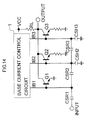
- variable amplifier of the present embodiment differs from the Figure 8 circuit in that when any of the common emitter transistors Q1 to Q3 is/are off, the base voltage(s) of the off common base transistors Q41, Q42, Q43 is/are controlled so as to force the base voltage(s) of the associated common base transistors Q41, Q42, Q43 to substantially 0 V.
- the common base transistors Q41, Q42, Q43 are actively turned off, further improving isolation.
- the variable amplifier of the present embodiment contains a base voltage control circuit controlling the base voltages VBB1 to VBB3 of the common base transistors Q41, Q42, Q43.
- the base voltage control circuit is coupled to the terminals VBB1, VBB2, VBB3 of the cascaded variable amplifier in Figure 8.
- Figure 10 shows the arrangement of the base voltage control circuit (voltage control section) connected to the Figure 8 circuit.
- the base voltage control circuit 2 differs from the base current control circuit 1 in Figure 2 as follows:
- the MOS transistor in the current switching section is an n-type field effect transistor (n-channel MOS transistor).
- a current mirror circuit is provided which contains a p-type field effect transistor (p-channel MOS transistor).
- the base current control circuit 1 in Figure 2 outputs current directly from the current switching section.
- the current switching section controls the incoming current flow, and the current mirror circuit changes the direction in which the current flows. This operation raises the maximum tolerable output voltage.
- a mirror circuit made up of a transistor QB3C and a transistor QB3M is coupled to the drain of the transistor QB1.
- Another mirror circuit made up of a transistor QB2C and a transistor QB2M is coupled to the drain of the transistor QB3.
- Another mirror circuit made up of a transistor QB1C and a transistor QB1M is coupled to the drain of the transistor QB4.
- a pair of resistors R1U, R1L is coupled to the mirror circuit containing QB1M.
- Another pair of resistors R2U, R2L is coupled to the mirror circuit containing QB2M.
- Another pair of resistors R3U, R3L is coupled to the mirror circuit containing QB3M.
- the resistors pairs are provided to convert current from the mirror circuit to voltage.
- the transistors QB1C, QB1M, QB2C, QB2M, QB3C, QB3M are all p-type field effect transistors (p-channel MOS transistors).
- the base voltage control circuit 2 generates the base currents IB1 to IB3 in accordance with the control voltage VCTRL and then generates the base voltages VBB1, VBB2, VBB3 from the base currents IB1 to IB for output through the terminals VB1, VB2, VB3.
- the currents IB1 to IB3 flowing respectively to the transistors QB4, QB3, QB1 shown in Figure 10 exhibit control voltage dependence as shown in Figure 3, similarly to the base current control circuit 1 shown in Figure 2.
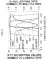
- the base current of a common emitter transistor (Q1 to Q3) and the base voltage of its cascaded common base transistor (Q41 to Q43) are indicated by the same kind of line (solid, dashed, and dash-dot).
- the base voltages VBB1 to VBB3 of the common base transistors Q41 to Q43 hardly vary when the common emitter transistors (Q1 to Q3) are in operation. It is therefore preferable if the currents through the resistors R1U, R1L, R2U, R2L, R3U, R3L are sufficiently large compared to necessary base currents.
- the circuit controlling the base voltages of the common base transistors Q41 to Q43 is not limited to the analog circuit shown in Figure 10 (base voltage control circuit 2).
- base voltage control circuit 2 Various alternatives are available, including analog circuits of other structures.
- Another alternative is a circuit which digitally generates a control signal under computer control and then generates the base voltages of the common base transistors Q41 to Q43 from the control signal using a D/A converter so as to control the unit amplifiers.
- variable amplifier of the present embodiment differs from the variable amplifier of embodiment 3 in that the base currents of the first group of transistors are varied and either the base or gate voltages of the multiple second transistors are varied. Further, the variable amplifier of the present embodiment is arranged so that the multiple common base or gate common transistors are actively turned off in accordance with the operation status of the common emitter transistors. The arrangement further improves the characteristics.
- variable amplifier of embodiment 4 Examining the characteristics of the variable amplifier of embodiment 4 in detail reveals that IIP3 drops with decreasing base currents IB1 to IB3 of the common emitter transistors Q1 to Q3.
- the variable amplifier of the present embodiment forces the common base transistors off before the base currents IB1 to IB3 of the common emitter transistors Q1 to Q3 fall to such levels where distortion may occur. Characteristics are thus improved.
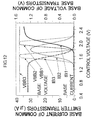
- Figure 12 shows the switching characteristics in connection with the base currents IB1 to IB3 of the common emitter transistors Q1 to Q3 and the control voltage VCTRL and also the switching characteristics in connection with the base voltages VBB1 to VBB3 of the common base transistors Q41 to Q43 and the control voltage VCTRL.
- the base voltages VBB1 to VBB3 of the common base transistors Q41 to Q43 are constant throughout a range of control voltage VCTRL where there are non-zero base currents IB1 to IB3 of the common emitter transistors Q1 to Q3.
- the base currents IB1 to IB3 of the common emitter transistors Q1 to Q3 completely go off (fall almost to 0 V) before the base voltages VBB1 to VBB3 of the common base transistors Q41 to Q43 fall almost to 0 V.
- Figure 13 shows the gain and IIP3 characteristics of the variable amplifier of the present embodiment (the gain is controlled only in a common emitter configuration) together with those of the variable amplifier of embodiment 4 (the distortion is removed in a common base configuration) for comparative purposes. It is understood that in the variable amplifier of the present embodiment, IIP3 degradation is greatly eased at a range of control voltage VCTRL at which the transistors Q1 to Q3 are switchable.
- variable amplifier of the present embodiment differs from the variable amplifier of embodiment 4 in that the base or gate voltages of the common base or common gate transistors are cut off before the base currents of the common emitter transistors are cut off as a control of the base currents of the common emitter transistors and the base or gate voltages of the common base or common gate transistors. Further, the control eases the development of distortion where the common emitter transistors turn off.
- all the unit amplifiers shared identical characteristics (gain and linearity). Individual unit amplifiers may have different characteristics. Achieving a large gain typically necessitates low noise, but not much linearity. A high degree of linearity is required, however, when the signal input has so large an amplitude that the amplifier is set to produce a small gain.
- Negative feedback is supplied to the transistors Q2, Q3 (amplifiers successive to an attenuator) by connecting a resistor or inductor to the emitters of the transistors Q2, Q3 for higher linearity.
- variable amplifier of the present embodiment differs from the variable amplifier of embodiment 1 in Figure 1 in that a resistor RE2 and a resistor RE3 are inserted respectively between the emitter of the transistor Q2 and ground and between the emitter of the transistor Q3 and ground to realize negative feedback.
- the transistor Q2 and the resistor RE2 form a unit amplifier, while the transistor Q3 and the resistor RE3 form another unit amplifier.
- a capacitor or a resistor between the base and the collector of the transistors Q2, Q3 may be placed to supply negative feedback to the transistors Q2, Q3.
- Coupling an inductor to an emitter is the best choice in terms of noise characteristics.
- Coupling a resistor to an emitter is a close second. Placing a resistor or a capacitor between the base and the collector of the transistors Q2, Q3 for negative feedback result in poor noise characteristics.
- Increasing current density for the transistors Q2, Q3 is also effective for further linearity improvements.
- the transistor Q1 that is the nearest to the input needs to have a low base resistance to achieve low noise. To this end, the transistor Q1 needs to have relatively large dimensions. To reduce current consumption in the transistor Q1 to a possible minimum, the current density of the transistor Q1 cannot be raised much.
- the specifications of the transistors Q2, Q3 located downstream to the attenuators AT1, AT2 are less strict in terms of noise characteristics. So, linearity is improved by reducing the transistors Q2, Q3 in dimension, hence adding to the current density of the transistors Q2, Q3.
- variable amplifier of the present embodiment differs from the variable amplifiers of any one of embodiments 1 through 5 in that the unit amplifiers each containing a transistor include two or more kinds of unit amplifier(s) with different characteristics.
- the amplifier will exhibit greatly improved overall characteristics by optimizing the characteristics of the individual amplifiers in accordance with characteristics.
- the unit amplifier (transistor Q1) that was the nearest to the input were required to exhibit large gain and low noise. To achieve the latter, reducing the base resistance of the transistor Q1 was inevitable, which in turn meant that the transistor Q1 had to come with added dimensions. To achieve large gain, the transistor Q1 needs to conduct a sufficiently large current. The transistor Q1 had to conduct a sufficiently large current also to achieve a sufficient level of linearity. The current consumption in the first unit amplifier (transistor Q1) therefore was rather large.
- linearity was an important characteristic for the two unit amplifier sections that were built around the transistors Q2, Q3 to which a signal was fed through the attenuators AT1, AT2.
- a way of achieving good linearity with these unit amplifier sections is to pass large current through the transistors Q2, Q3.
- the inputs of the unit amplifier sections were coupled to the attenuators AT1, AT2. This contributed to improvement of IIP3, a linearity indicator.
- the linearity of the unit amplifier sections could be improved by supplying negative feedback to the transistors Q2, Q3 or reducing the transistors Q2, Q3 in emitter area (thus increasing current density) for example. In short, when the noise characteristics are not very important, the linearity of the unit amplifier section can be improved even if the currents through the transistors Q2, Q3 are reduced.
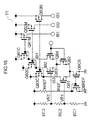
- variable amplifier of the present embodiment differs from the variable amplifier of embodiment 6 in Figure 14 primarily in that the base current control circuit 1 in Figure 2 is replaced with the base current control circuit 11 in Figure 15.
- the base current control circuit 11 in Figure 15 differs from the base current control circuit 1 in Figure 2 as follows:
- the MOS transistor in the current switching section is an n-type field effect transistor (n-channel MOS transistor).
- a current mirror circuit is provided which contains a p-type field effect transistor (p-channel MOS transistor).
- the base current control circuit 1 in Figure 2 outputs current directly from the current switching section.
- the current switching section controls the incoming current flow, and the current mirror circuit changes the direction in which the current flows.
- a mirror circuit made up of a transistor QB3C and a transistor QB3M is coupled to the drain of the transistor QB1.
- Another mirror circuit made up of a transistor QB2C and a transistor QB2M is coupled to the drain of the transistor QB3.
- Another mirror circuit made up of a transistor QB1C and a transistor QB1M is coupled to the drain of the transistor QB4.
- the transistors QB1C, QB1M, QB2C, QB2M, QB3C, QB3M are all p-type field effect transistors (p-channel MOS transistors).
- the base current control circuit 11 in Figure 15 permits free adjustment of individual base currents IB1 to IB3 through the transistors Q1 to Q3 by regulating the gate width of the transistors QB1M, QB2M, QB3M.
- the base current control circuit 11 controls the base currents IB1 to IB3 so that the combined current consumption in the transistors Q1 to Q3 changes in accordance with the ratio of the base currents IB1 to IB3 through the transistors Q1 to Q3.
- IIP3 is substantially in proportion to the collector current. Therefore, provided that the addition of the emitter resistors RE2, RE3 in Figure 14 to the variable amplifier in Figure 1 improves IIP3 by 3 dB while maintaining the collector currents, IIP3 remains substantially unchanged when the collector currents of the transistors Q2, Q3 is reduced to half in the variable amplifier in Figure 1. Therefore, in this case, for example, the base currents IB1, IB3 through the transistors Q1, Q3 should be controlled so that the collector current of the transistor Q3 has a maximum value half that of the collector current of the transistor Q1.
- the current consumption may be reduced in a variable amplifier when the input power is small, and raised relatively high when the input power is large and a high IIP3 is needed. This is applicable when that variable amplifier is used in a device of which the wiring design requires neither high IIP3 nor large gain when the input power is small, but requires high IIP3 when the input power is large.
- the present embodiment utilizes the simplest common emitter circuits equivalent to those in embodiment 1.
- the embodiment will exhibit further improvements in characteristics through cascade connections and modifications to the base voltage control circuit as in embodiments 2 to 5.
- variable amplifier of the present embodiment differs from the variable amplifier in any one of embodiments 1 through 6 in that the current consumption (collector current) in the first group of transistors differs from one transistor to another.
- the structure enables adjustment of current consumption in accordance with characteristics. The overall current consumption of the amplifier is thus reduced.
- FIG 16 is a block diagram of a mobile wireless terminal (e.g., mobile phone) containing a variable amplifier described in the preceding embodiments as a radio frequency variable gain amplifier (RFVGA).
- a mobile wireless terminal 10 of the present embodiment contains: an antenna 16; a bandpass filter (BPF) 17 limiting the bandwidth of the incoming radio frequency signal received by the antenna 16; a radio frequency variable gain amplifier (RFVGA) 12 amplifying the radio frequency signal filtered by the bandpass filter 17; a mixer (MIX) 13 mixing the radio frequency signal amplified by the radio frequency variable gain amplifier 12 with the oscillating signal output of the voltage control oscillator (VCO) 14 to convert the amplified radio frequency signal to a baseband signal; and a demodulator (DEMOD) 15 demodulating the baseband signal to recover the original signal.
- the radio frequency variable gain amplifier 12 is any one of the variable amplifiers of embodiments 1 to 7.
- the mobile wireless terminal 10 of such a construction is capable of directly coupling the bandpass filter (BPF) 17 to the input of the radio frequency variable gain amplifier, no longer requiring a balun which would be necessary in mobile wireless terminals based on conventional differential amplifier circuitry.
- BPF bandpass filter
- the elimination of the balun not only contributes to the overall circuit downsizing in the mobile wireless terminal, but also to reception power savings by eliminating the power dissipation in the balun. Therefore, the use of the radio frequency variable gain amplifier 12 in accordance with the present invention realizes a compact, high sensitivity mobile wireless terminal 10.
- the radio frequency variable gain amplifier 12 in accordance with the present invention can optimize the relationship between the gain and the current consumption in accordance with the characteristics of the mobile wireless terminal; thus, the resultant mobile wireless terminal consumes less power, allowing an extended time of operation.
- variable amplifier in accordance with the present invention may be used as an amplifier for the received signal in mobile wireless terminals. Further, the variable amplifier in accordance with the present invention may be used in terminals for the wireless communications system operating with high frequency signals, such as mobile phones.
Landscapes
- Engineering & Computer Science (AREA)
- Power Engineering (AREA)
- Control Of Amplification And Gain Control (AREA)
- Amplifiers (AREA)
Applications Claiming Priority (2)
| Application Number | Priority Date | Filing Date | Title |
|---|---|---|---|
| JP2003372674 | 2003-10-31 | ||
| JP2003372674A JP4252423B2 (ja) | 2003-10-31 | 2003-10-31 | 可変増幅器およびそれを用いた携帯無線端末 |
Publications (3)
| Publication Number | Publication Date |
|---|---|
| EP1528667A2 true EP1528667A2 (fr) | 2005-05-04 |
| EP1528667A3 EP1528667A3 (fr) | 2006-02-01 |
| EP1528667B1 EP1528667B1 (fr) | 2007-12-19 |
Family
ID=34420239
Family Applications (1)
| Application Number | Title | Priority Date | Filing Date |
|---|---|---|---|
| EP20040025774 Expired - Lifetime EP1528667B1 (fr) | 2003-10-31 | 2004-10-29 | Amplificateur variable et terminal mobile sans fil comprenant un tel amplificateur |
Country Status (4)
| Country | Link |
|---|---|
| EP (1) | EP1528667B1 (fr) |
| JP (1) | JP4252423B2 (fr) |
| CN (1) | CN1619950B (fr) |
| DE (1) | DE602004010771T2 (fr) |
Cited By (2)
| Publication number | Priority date | Publication date | Assignee | Title |
|---|---|---|---|---|
| EP1837989A1 (fr) * | 2006-03-24 | 2007-09-26 | Sharp Kabushiki Kaisha | Amplificateur à gain variable |
| US8571510B2 (en) | 2008-08-18 | 2013-10-29 | Qualcomm Incorporated | High linearity low noise receiver with load switching |
Families Citing this family (9)
| Publication number | Priority date | Publication date | Assignee | Title |
|---|---|---|---|---|
| JP2007104141A (ja) * | 2005-09-30 | 2007-04-19 | Mitsumi Electric Co Ltd | 可変利得回路 |
| JP2007142514A (ja) * | 2005-11-15 | 2007-06-07 | Nec Electronics Corp | 可変利得電力増幅器 |
| JP4902250B2 (ja) * | 2006-04-12 | 2012-03-21 | パナソニック株式会社 | 可変利得増幅器 |
| JP4956059B2 (ja) | 2006-06-12 | 2012-06-20 | ルネサスエレクトロニクス株式会社 | 可変利得増幅器 |
| JP2009005055A (ja) * | 2007-06-21 | 2009-01-08 | Niigata Seimitsu Kk | 利得可変増幅器 |
| JP2009005056A (ja) * | 2007-06-21 | 2009-01-08 | Niigata Seimitsu Kk | 利得可変増幅器 |
| JP5296809B2 (ja) * | 2009-01-13 | 2013-09-25 | パナソニック株式会社 | 可変利得増幅器およびそれを備えた高周波信号受信装置 |
| KR101090024B1 (ko) | 2009-08-26 | 2011-12-05 | 삼성전기주식회사 | Rf 가변 이득 증폭기 |
| CN110971205B (zh) | 2018-09-30 | 2022-08-09 | 华为技术有限公司 | 一种高线性度的可变增益放大器以及电子装置 |
Family Cites Families (8)
| Publication number | Priority date | Publication date | Assignee | Title |
|---|---|---|---|---|
| JPH0630422B2 (ja) * | 1985-11-15 | 1994-04-20 | 株式会社日立マイコンシステム | 電子スイツチ |
| JPH0239620A (ja) * | 1988-07-29 | 1990-02-08 | Nec Home Electron Ltd | 電子スイッチ回路 |
| JP3020511B2 (ja) * | 1989-05-24 | 2000-03-15 | 株式会社日立製作所 | 無線受信器 |
| JPH0396010A (ja) * | 1989-09-07 | 1991-04-22 | Nec Home Electron Ltd | 電子スイッチ回路 |
| JP3952114B2 (ja) * | 1999-07-27 | 2007-08-01 | ソニー株式会社 | 可変利得アンプ |
| JP4094239B2 (ja) * | 2001-02-19 | 2008-06-04 | 富士通株式会社 | 増幅器 |
| US6400227B1 (en) * | 2001-05-31 | 2002-06-04 | Analog Devices, Inc. | Stepped gain controlled RF driver amplifier in CMOS |
| JP3965284B2 (ja) * | 2001-09-11 | 2007-08-29 | 株式会社ルネサステクノロジ | 高周波増幅装置及び送受信装置 |
-
2003
- 2003-10-31 JP JP2003372674A patent/JP4252423B2/ja not_active Expired - Fee Related
-
2004
- 2004-10-29 DE DE200460010771 patent/DE602004010771T2/de not_active Expired - Lifetime
- 2004-10-29 EP EP20040025774 patent/EP1528667B1/fr not_active Expired - Lifetime
- 2004-11-01 CN CN 200410102328 patent/CN1619950B/zh not_active Expired - Fee Related
Cited By (3)
| Publication number | Priority date | Publication date | Assignee | Title |
|---|---|---|---|---|
| EP1837989A1 (fr) * | 2006-03-24 | 2007-09-26 | Sharp Kabushiki Kaisha | Amplificateur à gain variable |
| US7482879B2 (en) | 2006-03-24 | 2009-01-27 | Sharp Kabushiki Kaisha | Variable gain amplifier and communication apparatus |
| US8571510B2 (en) | 2008-08-18 | 2013-10-29 | Qualcomm Incorporated | High linearity low noise receiver with load switching |
Also Published As
| Publication number | Publication date |
|---|---|
| CN1619950B (zh) | 2011-06-08 |
| DE602004010771T2 (de) | 2008-12-04 |
| EP1528667B1 (fr) | 2007-12-19 |
| CN1619950A (zh) | 2005-05-25 |
| JP4252423B2 (ja) | 2009-04-08 |
| DE602004010771D1 (de) | 2008-01-31 |
| EP1528667A3 (fr) | 2006-02-01 |
| JP2005136846A (ja) | 2005-05-26 |
Similar Documents
| Publication | Publication Date | Title |
|---|---|---|
| US7164318B2 (en) | Continuous variable-gain low-noise amplifier | |
| US5872475A (en) | Variable attenuator | |
| US5999056A (en) | Variable gain amplifier using impedance network | |
| US6211737B1 (en) | Variable gain amplifier with improved linearity | |
| JP4956059B2 (ja) | 可変利得増幅器 | |
| US5945878A (en) | Single-ended to differential converter | |
| US6724259B2 (en) | Variable gain amplifier | |
| EP1484840B1 (fr) | Amplificateur radiofréquence à gain variable dont la linéarité est insensible au gain | |
| JP2007259297A (ja) | 可変利得増幅器及びこの可変利得増幅器を備えた通信装置 | |
| KR20040013229A (ko) | 가변 이득 저잡음 증폭기 | |
| EP1528667B1 (fr) | Amplificateur variable et terminal mobile sans fil comprenant un tel amplificateur | |
| EP1066683A1 (fr) | Amplificateur a gain variable, a grande dynamique | |
| US5867063A (en) | Gain distribution circuit | |
| US20020167355A1 (en) | Low-noise gain switching circuit using tapped inductor | |
| US6265942B1 (en) | Low power gain controlled amplifier with high dynamic range | |
| US20090027128A1 (en) | Variable gain amplifier | |
| US20060066399A1 (en) | Amplifier arrangement having an adjustable gain, and use thereof | |
| JP4312779B2 (ja) | 可変増幅器およびそれを用いた携帯無線端末 | |
| EP1349268B1 (fr) | Amplificateur MOS à gain variable | |
| EP1260015B1 (fr) | Amplificateur de gain a transconductance variable utilisant une paire differentielle de contre-reaction | |
| JP2006311623A5 (fr) | ||
| JP3219346B2 (ja) | 自動利得制御増幅器 | |
| CN115694382A (zh) | 可调整增益的放大电路 | |
| US6693492B2 (en) | Variable gain low-noise amplifier and method | |
| Nguyen et al. | A high-linearity low-noise reconfiguration-based programmable gain amplifier |
Legal Events
| Date | Code | Title | Description |
|---|---|---|---|
| PUAI | Public reference made under article 153(3) epc to a published international application that has entered the european phase |
Free format text: ORIGINAL CODE: 0009012 |
|
| AK | Designated contracting states |
Kind code of ref document: A2 Designated state(s): AT BE BG CH CY CZ DE DK EE ES FI FR GB GR HU IE IT LI LU MC NL PL PT RO SE SI SK TR |
|
| AX | Request for extension of the european patent |
Extension state: AL HR LT LV MK |
|
| PUAL | Search report despatched |
Free format text: ORIGINAL CODE: 0009013 |
|
| AK | Designated contracting states |
Kind code of ref document: A3 Designated state(s): AT BE BG CH CY CZ DE DK EE ES FI FR GB GR HU IE IT LI LU MC NL PL PT RO SE SI SK TR |
|
| AX | Request for extension of the european patent |
Extension state: AL HR LT LV MK |
|
| RIC1 | Information provided on ipc code assigned before grant |
Ipc: H03F 1/22 20060101ALI20051215BHEP Ipc: H03F 1/18 20060101AFI20050210BHEP Ipc: H03F 3/19 20060101ALI20051215BHEP |
|
| 17P | Request for examination filed |
Effective date: 20060712 |
|
| 17Q | First examination report despatched |
Effective date: 20060804 |
|
| AKX | Designation fees paid |
Designated state(s): DE FR GB |
|
| GRAP | Despatch of communication of intention to grant a patent |
Free format text: ORIGINAL CODE: EPIDOSNIGR1 |
|
| GRAS | Grant fee paid |
Free format text: ORIGINAL CODE: EPIDOSNIGR3 |
|
| GRAA | (expected) grant |
Free format text: ORIGINAL CODE: 0009210 |
|
| AK | Designated contracting states |
Kind code of ref document: B1 Designated state(s): DE FR GB |
|
| REG | Reference to a national code |
Ref country code: GB Ref legal event code: FG4D |
|
| REF | Corresponds to: |
Ref document number: 602004010771 Country of ref document: DE Date of ref document: 20080131 Kind code of ref document: P |
|
| ET | Fr: translation filed | ||
| PLBE | No opposition filed within time limit |
Free format text: ORIGINAL CODE: 0009261 |
|
| STAA | Information on the status of an ep patent application or granted ep patent |
Free format text: STATUS: NO OPPOSITION FILED WITHIN TIME LIMIT |
|
| 26N | No opposition filed |
Effective date: 20080922 |
|
| PGFP | Annual fee paid to national office [announced via postgrant information from national office to epo] |
Ref country code: FR Payment date: 20121018 Year of fee payment: 9 Ref country code: DE Payment date: 20121024 Year of fee payment: 9 |
|
| PGFP | Annual fee paid to national office [announced via postgrant information from national office to epo] |
Ref country code: GB Payment date: 20121024 Year of fee payment: 9 |
|
| GBPC | Gb: european patent ceased through non-payment of renewal fee |
Effective date: 20131029 |
|
| PG25 | Lapsed in a contracting state [announced via postgrant information from national office to epo] |
Ref country code: GB Free format text: LAPSE BECAUSE OF NON-PAYMENT OF DUE FEES Effective date: 20131029 |
|
| REG | Reference to a national code |
Ref country code: DE Ref legal event code: R119 Ref document number: 602004010771 Country of ref document: DE Effective date: 20140501 |
|
| REG | Reference to a national code |
Ref country code: FR Ref legal event code: ST Effective date: 20140630 |
|
| PG25 | Lapsed in a contracting state [announced via postgrant information from national office to epo] |
Ref country code: DE Free format text: LAPSE BECAUSE OF NON-PAYMENT OF DUE FEES Effective date: 20140501 Ref country code: FR Free format text: LAPSE BECAUSE OF NON-PAYMENT OF DUE FEES Effective date: 20131031 |