EP1528436A1 - Ladesystem für ein Bilderzeugungsgerät - Google Patents
Ladesystem für ein Bilderzeugungsgerät Download PDFInfo
- Publication number
- EP1528436A1 EP1528436A1 EP04256691A EP04256691A EP1528436A1 EP 1528436 A1 EP1528436 A1 EP 1528436A1 EP 04256691 A EP04256691 A EP 04256691A EP 04256691 A EP04256691 A EP 04256691A EP 1528436 A1 EP1528436 A1 EP 1528436A1
- Authority
- EP
- European Patent Office
- Prior art keywords
- region
- charging
- bearing member
- image bearing
- charge
- Prior art date
- Legal status (The legal status is an assumption and is not a legal conclusion. Google has not performed a legal analysis and makes no representation as to the accuracy of the status listed.)
- Granted
Links
- 238000003384 imaging method Methods 0.000 claims abstract description 65
- 238000000034 method Methods 0.000 claims description 15
- 230000007246 mechanism Effects 0.000 claims description 14
- 238000012544 monitoring process Methods 0.000 claims description 2
- 238000012545 processing Methods 0.000 description 17
- 239000007788 liquid Substances 0.000 description 6
- 239000000463 material Substances 0.000 description 6
- 230000007547 defect Effects 0.000 description 5
- 238000010586 diagram Methods 0.000 description 5
- 238000003860 storage Methods 0.000 description 5
- 238000009413 insulation Methods 0.000 description 4
- 238000011161 development Methods 0.000 description 3
- 239000012530 fluid Substances 0.000 description 3
- 230000002452 interceptive effect Effects 0.000 description 3
- 239000003550 marker Substances 0.000 description 3
- 229920000642 polymer Polymers 0.000 description 3
- 238000011109 contamination Methods 0.000 description 2
- 238000004519 manufacturing process Methods 0.000 description 2
- 238000012546 transfer Methods 0.000 description 2
- CBENFWSGALASAD-UHFFFAOYSA-N Ozone Chemical compound [O-][O+]=O CBENFWSGALASAD-UHFFFAOYSA-N 0.000 description 1
- 229910000831 Steel Inorganic materials 0.000 description 1
- 238000009825 accumulation Methods 0.000 description 1
- 230000015572 biosynthetic process Effects 0.000 description 1
- 230000015556 catabolic process Effects 0.000 description 1
- 238000004140 cleaning Methods 0.000 description 1
- 230000003247 decreasing effect Effects 0.000 description 1
- 238000000151 deposition Methods 0.000 description 1
- 238000001914 filtration Methods 0.000 description 1
- 230000003287 optical effect Effects 0.000 description 1
- 230000002093 peripheral effect Effects 0.000 description 1
- 239000004065 semiconductor Substances 0.000 description 1
- 239000010959 steel Substances 0.000 description 1
Images




Classifications
-
- G—PHYSICS
- G03—PHOTOGRAPHY; CINEMATOGRAPHY; ANALOGOUS TECHNIQUES USING WAVES OTHER THAN OPTICAL WAVES; ELECTROGRAPHY; HOLOGRAPHY
- G03G—ELECTROGRAPHY; ELECTROPHOTOGRAPHY; MAGNETOGRAPHY
- G03G15/00—Apparatus for electrographic processes using a charge pattern
- G03G15/02—Apparatus for electrographic processes using a charge pattern for laying down a uniform charge, e.g. for sensitising; Corona discharge devices
- G03G15/0208—Apparatus for electrographic processes using a charge pattern for laying down a uniform charge, e.g. for sensitising; Corona discharge devices by contact, friction or induction, e.g. liquid charging apparatus
- G03G15/0216—Apparatus for electrographic processes using a charge pattern for laying down a uniform charge, e.g. for sensitising; Corona discharge devices by contact, friction or induction, e.g. liquid charging apparatus by bringing a charging member into contact with the member to be charged, e.g. roller, brush chargers
-
- G—PHYSICS
- G03—PHOTOGRAPHY; CINEMATOGRAPHY; ANALOGOUS TECHNIQUES USING WAVES OTHER THAN OPTICAL WAVES; ELECTROGRAPHY; HOLOGRAPHY
- G03G—ELECTROGRAPHY; ELECTROPHOTOGRAPHY; MAGNETOGRAPHY
- G03G15/00—Apparatus for electrographic processes using a charge pattern
- G03G15/02—Apparatus for electrographic processes using a charge pattern for laying down a uniform charge, e.g. for sensitising; Corona discharge devices
- G03G15/0208—Apparatus for electrographic processes using a charge pattern for laying down a uniform charge, e.g. for sensitising; Corona discharge devices by contact, friction or induction, e.g. liquid charging apparatus
- G03G15/025—Apparatus for electrographic processes using a charge pattern for laying down a uniform charge, e.g. for sensitising; Corona discharge devices by contact, friction or induction, e.g. liquid charging apparatus by bringing a charging member in the vicinity with the member to be charged, e.g. proximity charging, forming microgap
-
- G—PHYSICS
- G03—PHOTOGRAPHY; CINEMATOGRAPHY; ANALOGOUS TECHNIQUES USING WAVES OTHER THAN OPTICAL WAVES; ELECTROGRAPHY; HOLOGRAPHY
- G03G—ELECTROGRAPHY; ELECTROPHOTOGRAPHY; MAGNETOGRAPHY
- G03G15/00—Apparatus for electrographic processes using a charge pattern
- G03G15/02—Apparatus for electrographic processes using a charge pattern for laying down a uniform charge, e.g. for sensitising; Corona discharge devices
- G03G15/0275—Arrangements for controlling the area of the photoconductor to be charged
Definitions
- aspects of the invention relate to hard imaging device charging systems, liquid electrophotography charging systems, hard imaging apparatuses, and hard imaging device electrophotography charging methods.
- Charge rollers are used to charge a photoconductor in hard imaging systems (e.g., laser-printer imaging systems). Similar to Scorotron/Corona charging, charge rollers use air ionization to charge a photoconductor. However, a charge roller has increased charging efficiency (close to 100% charging efficiency) and uses lower voltages ( ⁇ 1500V) compared with Scorotron charging ( ⁇ 6500V). Charge rollers are typically used in dry (e.g., toner-based) electrophotography processes. In liquid electrophotography processes using a photoconductor having a seam, charge rollers may create print quality defects due to accumulation of imaging fluid in defects or wrap-over sections (e.g., seam regions) on the photoconductor.
- Movement of the charge roller over a section of the photoconductor having an uneven layer of imaging fluid causes breakdown of the imaging fluid thereby depositing excess imaging oil on the photoconductor during each rotation of the charge roller.
- the extra imaging oil not only causes disturbance of normal imaging processes but also causes disruption of the Paschen curve and the photoconductor charging voltages, thereby leading to non-uniformity in charging and print quality defects.
- the charge roller interacts with the imaging oil and creates a sticky polymer that may coat the photoconductor.
- the above drawbacks may contribute to photoconductor quality issues by interfering with the photoconductor/blanket image transfer, interfering with image development, and interfering with cleaning of the photoconductor.
- the above drawbacks may also cause problems relating to photoconductor lateral conductivity, and uneven photoconductor charging. As a result, lifetime of consumables may decrease and the printing cost per page may increase.
- the created polymer is transferred to the photoconductor at distances corresponding to the circumference of the charge roller.
- the charge roller during each rotation rolls some of the polymer onto the photoconductor, and the end result is a defect having a shape of the uneven imaging oil layer causing formation of images having decreasing intensities with increasing rotations of the charge roller.
- Improved imaging devices and methods are desired.
- At least some embodiments of the invention relate to hard imaging device charging systems, liquid electrophotography charging systems, hard imaging apparatuses, and hard imaging device electrophotography charging methods.
- a hard imaging device charging system may include a first charging device configured to charge a respective first region of a cylindrical image bearing member used to form latent images during hard imaging operations of the hard imaging device.
- the charging system may also include a second charging device configured to charge a respective second region of the cylindrical image bearing member used to form latent images during hard imaging operations of the hard imaging device.
- the first and second regions may have different radii from a central axis of the cylindrical image bearing member.
- a hard imaging device electrophotography charging method includes charging a first region of a photoconductor using a first charging device, the photoconductor may be used to form latent images during hard imaging operations of the hard imaging device.
- the method may also include charging a second region of the photoconductor using a second charging device.
- the first charging may include charging an imaging region of the photoconductor of the hard imaging device, and the second charging may include charging a non-imaging region of the photoconductor.
- Fig. 1 is an exemplary diagram of a hard imaging device in accordance with one embodiment.
- Fig. 2 is a high-level block diagram of a hard imaging device according to one embodiment.
- Fig. 3 is a functional block diagram of a controller of the hard imaging device according to one embodiment.
- Fig. 4 is a functional schematic illustrating an exemplary electrophotographic process according to one embodiment.
- Figs. 4A-4C shows exemplary schematics illustrating arrangements of a photoconductor according to various embodiments.
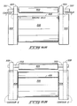
- Figs. 5A-5B show exemplary configurations to provide clearances between primary and secondary charge rollers and the photoconductor, using passive mechanisms according to various embodiments.
- Figs. 6A-6B are side view schematics for providing predetermined clearances between primary and secondary charge rollers and the photoconductor according to various embodiments.
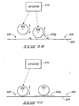
- Figs. 7A-7C show exemplary configurations to provide clearances between primary and secondary charge rollers and the photoconductor, using active mechanisms according to various embodiments.
- an exemplary hard imaging device 100 is shown in accordance with one embodiment of the invention.
- the hard imaging device 100 may be a laser printer.
- Other configurations configured to form hard images upon a media 212 are possible, and include for example, multi-function peripherals, copiers, facsimile devices, etc.
- Hard imaging device 100 may be embodied as a device configured to use a dry or liquid marking agent (e.g., toner) in exemplary configurations.
- a dry or liquid marking agent e.g., toner
- Fig. 2 illustrates an exemplary high-level block diagram of the hard imaging device 100 in accordance with one embodiment of the invention.
- the depicted hard imaging device 100 configured as a laser printer includes a controller 202, a formatter 203, a laser scanning apparatus 204, an image bearing member (e.g., in one embodiment configured as a photoconductor) 206, a charging assembly 208, and a developer/fusing assembly 210 configured to form hard images on media 212.
- an image bearing member e.g., in one embodiment configured as a photoconductor
- a charging assembly 208 e.g., a charging assembly
- developer/fusing assembly 210 configured to form hard images on media 212.
- the controller 202 may be configured to control operations of individual components (e.g., 203, 204, 206, 208, 210) of the hard imaging device 100.
- the controller 202 may be configured to control operations of the charging assembly 208.
- exemplary operations of the charging assembly 208 include actuation/movement of primary and secondary charge rollers (e.g., reference numerals 402 and 404 of Fig. 4) of the charging assembly 208 in order to provide predetermined clearances between select charge rollers and the image bearing member 206. Further details of controller 202 are described below at Fig. 3.
- Formatter 203 may be configured to perform image data processing operations (e.g., rasterization) of data received from an external source (not shown), internally generated, or otherwise accessed.
- image data processing operations e.g., rasterization
- the laser scanning apparatus 204 may be configured to scan information formatted by the formatter 203 onto image bearing member 206 to form latent images.
- the laser scanning apparatus 204 may emit a light beam to scan information in one embodiment.
- the laser scanning apparatus 204 is alternatively referred to as a scanning device.
- Image bearing member 206 includes a rotating imaging surface configured to receive information scanned by the laser scanning apparatus 204 in one embodiment.
- An exemplary image bearing member embodied as image bearing member 206 comprises a steel cylinder having an outwardly exposed layer of photoconductive material. Other embodiments of image bearing member 206 are possible.
- One or more lines of information (e.g., information formatted by the formatter 203) may be scanned by laser scanning apparatus 204 onto image bearing member 206 to form latent images on the imaging surface of the image bearing member 206 during hard imaging operations of the hard imaging device 100.
- the charging assembly 208 may be configured to charge image bearing member 206 to enable forming of latent images on the image bearing member 206.
- the charging assembly 208 may have a plurality of charging devices (e.g., a first charging device 402, a second charging device 404 (Fig. 4)).
- the charging assembly 208 is alternatively referred to herein as a charging system.
- First and second charging devices 402, 404 may also be referred to as charge rollers or members. Charge rollers 402, 404 are positioned adjacent to the image bearing member 206 to charge respective regions of the image bearing member 206 as described further below.
- the developer/fusing assembly 210 may be configured to develop latent images formed on the image bearing member 206 using a marking agent (e.g., dry or liquid toner), and transfer and fuse the developed image to media 212 (e.g., hard-imaging media such as paper, transparencies, etc.).
- a marking agent e.g., dry or liquid toner
- media 212 e.g., hard-imaging media such as paper, transparencies, etc.
- Fig. 3 is a functional block diagram of exemplary controller 202 configured to control operations (e.g., actuation/movement of charge rollers 402, 404 (Fig. 4)) of the charging assembly 208 or other components of device 100 in accordance with an exemplary embodiment.
- the controller 202 includes processing circuitry 302, a storage device 304 having a database 306, and an interface 308. Other implementations of the controller 202 are possible.
- Processing circuitry 302 may be configured in one embodiment to issue command signals to an actuator 510 (Fig. 7A) to control movement of one or both of primary and secondary charge rollers 402, 404 (Fig. 7A), respectively, to provide predetermined clearances (e.g., charging clearance, spaced clearance) between image bearing member 206 and charge rollers 402, 404 (Fig. 7A), respectively.
- processing circuitry 302 may be configured to issue command signals to actuator 510 (Fig. 7A) to control movement of the primary and/or secondary charge rollers 402, 404 (Fig. 7A), respectively, to provide predetermined clearances with respect to different regions or areas of the image bearing member 206.
- processing circuitry 302 may comprise circuitry configured to execute provided programming.
- processing circuitry 302 may be implemented as a microprocessor or other structure configured to execute executable instructions of programming including, for example, software and/or firmware instructions.
- Other exemplary embodiments of processing circuitry 302 include hardware logic, PGA, FPGA, ASIC, and/or other structures. These examples of processing circuitry 302 are for illustration and other configurations are possible for implementing operations discussed herein.
- the storage device 304 may be configured to store predetermined value(s) corresponding to clearances between primary charge roller 402, secondary charge roller 404, and image bearing member 206, respectively.
- the predetermined clearance value(s) may be stored in database 306 of the storage device 304.
- the predetermined value(s) may be stored in the form of a table in the database 306 of the storage device 304, and the stored information may be configured for retrieval by the processing circuitry 302.
- the storage device 304 may also be configured to store electronic data, file systems having one or more electronic files, programming such as executable instructions (e.g., software and/or firmware for use by processing circuitry 302), and/or other digital information and may include processor-usable media.
- Processor-usable media includes any article of manufacture which can contain, store, or maintain programming, data and/or digital information for use by or in connection with an instruction execution system including processing circuitry in the exemplary embodiment.
- exemplary processor-usable media may include any one of physical media such as electronic, magnetic, optical, electromagnetic, infrared or semiconductor media.
- processor-usable media include, but are not limited to, a portable magnetic computer diskette, such as a floppy diskette, zip disk, hard drive, random access memory, read only memory, flash memory, cache memory, and/or other configurations capable of storing programming, data, or other digital information.
- a portable magnetic computer diskette such as a floppy diskette, zip disk, hard drive, random access memory, read only memory, flash memory, cache memory, and/or other configurations capable of storing programming, data, or other digital information.
- Interface 308 may be configured to communicate electronic data externally of the controller 202, for example, received from external devices, with formatter 203 to perform rasterization tasks, and communicate control signals to an actuator 510 (Fig. 7A) to control movement of charge rollers 402, 404 (Fig. 7A).
- Fig. 4 is a functional schematic illustrating exemplary electrophotography aspects. For example, charging of a image bearing member 206 using a charging assembly 208 in accordance with one embodiment is shown.
- the charging assembly 208 is positioned adjacent to the image bearing member 206 in order to charge respective plural regions of the image bearing member 206.
- the charging assembly 208 includes primary and secondary charge rollers 402, 404 to charge respective regions of the image bearing member 206.
- a voltage supply apparatus 410 is configured to supply voltage to the charging assembly 208 (e.g., primary and secondary charge rollers 402, 404, respectively) to charge respective regions of the image bearing member 206.
- image bearing member 206 comprises a plurality of different regions.
- the plural regions may correspond to regions of an outer surface of image bearing member 206 having different radii or otherwise spaced different distances from a central axis 207.
- image bearing member 206 may comprise first and second regions/areas 408, 406 of different radii.
- photoconductive material of image bearing member 206 may be provided in a layer 409 about a cylinder.
- the layer 409 may be joined at a seam region or area.
- a second region 406 corresponds to the seam area created during wrapping of imaging or photoconductive material 409 on the cylindrical drum to form the image bearing member 206.
- a first region 408 corresponds to an area other than the region 406 of the image bearing member 206.
- region 408 of the image bearing member 206 is configured to form latent images during hard imaging operations of the hard imaging device 100 (Fig. 1) and may be referred to as an image area or region.
- region 408 of the image bearing member 206 may be referred to as an image area or region.
- Other embodiments are possible.
- roller 402 only charges region 408 and roller 404 only charges region 406.
- the primary charge roller 402 may be configured to contact region 408 of the image bearing member 206 in one embodiment or maintain a clearance (e.g., 19 microns or less) with region 408 of the image bearing member 206 according to another embodiment while still providing charging.
- a position for charging using rollers 402 or 404 may be referred to as a charging position and may include spaced clearance or actual contact of the roller with the respective region of the image bearing member 206.
- the primary charge roller 402 may be configured to maintain a desired clearance (e.g., greater than 200 microns) with region 406 of the image bearing member 206 in order to avoid charging of region 406.
- a position used to avoid charging may be referred to as an insulation or insulating position.
- the secondary charge roller 404 may be may be provided in the charging position relative to region 406.
- the secondary charge roller 404 may be provided in an insulation position with respect to region 408 in order to avoid charging of region 408.
- Figs. 4A-4C shows exemplary schematics illustrating arrangements of region 406 with respect to region 408 of image bearing member 206 according to various embodiments.
- like elements are identified with like numerals, but with a suffix added.
- Fig. 4A illustrates an exemplary arrangement having region 406a having a reduced radius (R2 a ) compared to radius (R1 a ) of region 408a (e.g., region 406a arranged at a lower level compared to region 408a on image bearing member 206 (R2 a ⁇ R1 a )).
- Fig. 4C illustrates an exemplary arrangement having region 406c having a larger radius (R2 c ) compared to radius (R1 c ) of region 408c (e.g., region 406 is arranged at a higher level compared to region 408 on image bearing member 206 (R2c>R1c)).
- a given region 406 or 408 may or may not have a constant radius throughout an entire respective region in the described embodiments.
- Figs. 5A-5B show exemplary arrangements schematics to provide predetermined positions (e.g., charging or insulation positions) of rollers 402, 404, with respect to respective areas 408, 406 using passive or passively controlled mechanisms (e.g., drive rollers, reference disks) to provide charging of respective areas 408, 406 by only respective rollers 402, 404.
- Passively controlled may refer to controlling positions between charge rollers 402, 404 and respective regions 408, 406 of image bearing member 206 using passive mechanisms such as drive rollers (e.g., 504, 508), reference disks 506, etc.
- Passive mechanisms may refer to configurations not relying upon control from provided processing circuitry or other external control.
- roller 402 only charges region 408 and roller 404 only charges region 406.
- the primary and secondary charge rollers 402, 404 may be individually provided within the charging positions with respect to areas 408, 406 of the image bearing member 206 to provide appropriate charging.
- the primary charge roller 402 includes end portions 501 of a cylindrical shaft configured to be received by drive members 504 (e.g., drive rollers), and drive members 504 are configured to roll on a respective contour path (e.g., contour 1 of Fig. 6A) of members 506 (e.g., reference disks) of the image bearing member 206 in order to provide predetermined charging and insulated positioning of primary charge roller 402 with respect to areas 408, 406, respectively.
- drive members 504 e.g., drive rollers
- members 506 e.g., reference disks
- end portions 502 of a cylindrical shaft of the secondary charge roller 404 are received in drive members 508 (e.g., drive rollers), and members 508 are configured to roll on a respective contour path (e.g., contour 2 of Fig. 6A) of members 506 (e.g., reference disks) of the image bearing member 206 to provide predetermined charging and insulated positioning of secondary charge roller 404 with respect to areas 408, 406, respectively.
- drive members 508 may be positioned offset relative to drive members 504 in order to follow different respective contour paths on a surface of members 506.
- each set of drive members 504, 508, respectively may be configured to ride on a distinct section (e.g., contour 1, contour 2) of a surface of members 506 of the image bearing member 206 to provide desired charging or insulated positioning during charging of the image bearing member 206.
- Contours 1 and 2 illustrated in Figs. 5A-5B are shown to be merely exemplary. Other contour arrangements to maintain clearances between charge rollers 402, 404 and respective areas of image bearing member are possible.
- passive mechanisms e.g., drive rollers 504, 508, members 506 may be configured to selectively control the first and second charge rollers 402, 404 (Fig. 4) corresponding to rotation of regions 408, 406 (Fig. 4) of the image bearing member 206 during rotation of the image bearing member 206 and member 506 therewith.
- Figs. 6A-6B show side view schematics for providing predetermined clearances between primary and secondary charge rollers 402, 404 and image bearing member 206 in order to only charge respective regions (e.g., 408, 406) of the image bearing member 206 according to exemplary embodiments.
- Fig. 6A illustrates positioning of drive members 504, 508 on surfaces of members 506 of image bearing member 206 in order to provide predetermined positioning of charge rollers 402, 404 and image bearing member 206 in order to only charge areas 408, 406, respectively, of the image bearing member 206 of Fig. 4A.
- region 406a has reduced radii R2a compared to region 408a having radius R1 a (Fig. 4A).
- members 506 may be configured via varied contour paths to enable the primary charge roller 402 to charge only region 408 of the image bearing member 206.
- Members 506 may also be configured to enable the secondary charge roller 404 to charge only region 406 of the image bearing member 206.
- drive member 504 may be configured to follow contour 1 (e.g., a first section of a surface of member 506) to charge only region 408 while drive member 508 may be configured to follow contour 2 (e.g., a second section of a surface of member 506) to enable the secondary charge roller 404 to charge only region 408 of the image bearing member 206 (Fig. 4).
- Contour 2 of member 506 has a reduced radius R2 at region 406 of image bearing member 206 than radius R1 of contour 1, the radii being measured from a central axis 507 to respective contour surfaces of member 506.
- Drive member 508 may be configured to move the secondary charge roller 404 (Fig.
- roller 404 is provided at an insulation position with respect to region 408.
- Contour 1 corresponding to a circular circumference of member 506 provides roller 402 in the charging position relative to region 408 and in the insulating position relative to region 406.
- region 406 is arranged having a larger radius when compared to region 408 of the image bearing member 206 (Fig. 4C).
- drive member 504 may be configured to follow contour 3 (e.g., a first section of a surface of member 506a) to enable the primary charge roller 402 to only charge region 408.
- Drive member 508 may be configured to follow contour 4 (e.g., a second section of a surface of member 506a) to enable the secondary charge roller 404 to only charge region 406 of the image bearing member 206.
- region 406 has a larger radius R2c compared to region 408 having radius R1 c .
- Contour 3 of member 506 has larger radii R2 at region 406 of image bearing member 206 than radius R1 of contour 4, the radii measured from a central axis 507 to respective contour surfaces of member 506.
- Drive member 506 may be configured to move the secondary charge roller 404 from a charging position 504a for charging region 408 to the insulated position 504 with respect to region 406.
- Member 508 does not move in a radial direction in the configuration of Fig. 6B but is located to provide roller 404 in an insulated position with respect to region 408 and a charging position with respect to region 406.
- member 506a may be altered to provide contour 4 of Fig.
- contour 2 to provide inward radial movement of roller 404 to selectively charge region 406 and move to the insulated position to not charge region 408.
- the indent e.g., shown in contour 2 of Fig. 6A
- size (e.g., diameter) of the drive members 504, 508 may be varied to provide predetermined positioning of rollers 402, 404 with respect to regions 408, 406.
- positions of members 506 of the image bearing member 206 are desired to be of circular shape as other processes (e.g., developing, fixing, etc.) of the hard imaging device 100 (Fig. 1) may rely on the image bearing member 206 for precision spacing.
- one portion of members 506 may be circular for other processes, and another contoured of different radii to control positioning of rollers 402, 404.
- Figs. 7A-7C show exemplary schematics to control positioning of primary charge roller 402 and secondary charge roller 404 with respect to regions 408, 406 using actively controlled mechanisms (e.g., solenoid driven actuators, stepper motor, or such external load systems, etc.) in accordance with various embodiments.
- actively controlled is generally defined as controlling positioning of charge rollers 402, 404 using actively controlled mechanisms as motors, solenoid actuators, etc.
- FIG. 7A there is shown an exemplary schematic to charge areas 408, 406, respectively, of image bearing member 206 using primary and secondary charge rollers 402, 404, respectively, in accordance with one embodiment.
- Image bearing member 206 is configured to rotate in the indicated process direction in the depicted embodiment. Desired positioning of rollers 402, 404 is provided by selectively moving one or both of primary and secondary charge rollers 402, 404, using one or more actuator 510 (only movement of roller 404 is shown in Fig. 7A).
- a single actuator 510 is shown to control movement of charge roller 404.
- actuator 510 may be a solenoid control actuator having a motor to move charge roller 404 (or roller 402) into desired positions.
- a spring-loaded mechanism (not shown) may be provided to enable movement of one or both of charge rollers 402, 404 towards or away from the image bearing member 206. The spring-loaded mechanism may be coupled to the actuator 510 to establish desired positioning.
- area 406a of image bearing member 206 is provided at a reduced radius compared to a radius of region 408 of image bearing member 206.
- Actuator 510 may be configured such that roller 404 is moved to a position 404a to only charge region 406a while the charge roller 402 is provided at a fixed position to charge only region 408 and to avoid charging region 406a.
- the actuator 510 may be configured to lower (e.g., move towards the image bearing member 206) the secondary charge roller 404 to charge region 406 at the depicted position 404a.
- Processing circuitry 302 (Fig. 3) of controller 202 may be configured to issue command signals to actuator 510 to control movement (e.g., towards or away from the image bearing member 206) of the secondary charge roller 404.
- the processing circuitry 302 (Fig. 3) may be configured to issue timing signals to actuator 510 to appropriately time such movement of the charge roller 404.
- processing circuitry 302 (Fig. 3) may be configured to monitor rotation of image bearing member 206 and issue command signals to actuator 510 to lower or raise the secondary charge roller 404 (or roller 402) as appropriate.
- Fig. 7B shows an exemplary schematic for charging image bearing member 206 having areas 408, 406b arranged at a same level (e.g., spaced at substantially constant radius of Fig. 4B) on the image bearing member 206 in accordance with an exemplary embodiment.
- Actuator 510 may be configured to move both primary and secondary charge rollers 402, 404 to charge only respective areas 408, 406 of the image bearing member 206.
- primary charge roller 402 is controlled to charge region 408 and be insulated from charging of region 406.
- the secondary charge roller 404 may be configured to charge region 406 and be insulated from region 408. Movement of charge rollers 402, 404 to charge areas 408, 406, respectively, may be controlled using actuator 510 responsive to control of processing circuitry 302 in one embodiment.
- Fig. 7C shows an exemplary schematic for charging image bearing member 206 having region 406 arranged at a higher level (e.g., increased radius as shown in Fig. 4C) when compared to region 408 on the image bearing member 206, according to one embodiment.
- charging of areas 408, 406 of the image bearing member 206 may be performed by arranging the secondary charge roller 404 to charge region 406 while be insulated from region 408.
- Roller 404 may be provided at fixed or moveable positions in exemplary embodiments.
- Roller 402 may be controlled to move between the charging and insulated positions to charge only region 402 in one embodiment.
- Processing circuitry 302 may be configured to issue command signals to actuator 510 to control movement of primary and/or secondary rollers 402, 404, respectively, as described above (e.g., responsive to monitoring rotation of image bearing member 206) or using other control.
- Exemplary advantages of some embodiments include providing a clearance between charge rollers and an image bearing member to reduce chances of damage to the charge rollers due to contact with the image bearing member. Since no direct charging of the image bearing member occurs in embodiments having a clearance between the charge rollers and the image bearing member, high charging uniformity in both in-scan and cross-scan directions may be possible. Solutions provided by some embodiments provide a charging system which is more robust to misalignments and material defects during manufacturing. Other advantages of using charge rollers to charge a image bearing member include efficiencies related to cost, size, and Ozone generation rate.
- some exemplary hard imaging device embodiments utilize image bearing members having a seam area.
- image bearing members having a seam area.
- Usage of a plurality of charge rollers, one dedicated to charge the seam area as described in some embodiments herein, facilitates filtering of contamination materials, such as imaging oil, and reduces the introduction of the contamination materials into the image area of the image bearing member.
Landscapes
- Physics & Mathematics (AREA)
- Engineering & Computer Science (AREA)
- Plasma & Fusion (AREA)
- General Physics & Mathematics (AREA)
- Electrostatic Charge, Transfer And Separation In Electrography (AREA)
Applications Claiming Priority (2)
| Application Number | Priority Date | Filing Date | Title |
|---|---|---|---|
| US700963 | 1991-05-16 | ||
| US10/700,963 US7035572B2 (en) | 2003-10-31 | 2003-10-31 | Hard imaging device charging systems, electrophotography charging systems, hard imaging apparatuses, and hard imaging device electrophotography charging methods |
Publications (2)
| Publication Number | Publication Date |
|---|---|
| EP1528436A1 true EP1528436A1 (de) | 2005-05-04 |
| EP1528436B1 EP1528436B1 (de) | 2011-10-19 |
Family
ID=34423471
Family Applications (1)
| Application Number | Title | Priority Date | Filing Date |
|---|---|---|---|
| EP04256691A Expired - Lifetime EP1528436B1 (de) | 2003-10-31 | 2004-10-29 | Ladesystem für ein Bilderzeugungsgerät |
Country Status (2)
| Country | Link |
|---|---|
| US (1) | US7035572B2 (de) |
| EP (1) | EP1528436B1 (de) |
Cited By (1)
| Publication number | Priority date | Publication date | Assignee | Title |
|---|---|---|---|---|
| US8731436B2 (en) | 2011-06-01 | 2014-05-20 | Hewlett-Packard Development Company, L.P. | Positioning system for a charge roller and printer using the same |
Families Citing this family (8)
| Publication number | Priority date | Publication date | Assignee | Title |
|---|---|---|---|---|
| KR100553907B1 (ko) * | 2003-12-15 | 2006-02-24 | 삼성전자주식회사 | 스페이서가 구비된 감광드럼 및 이를 구비한 전자사진방식화상형성장치 |
| US7835668B2 (en) * | 2004-11-24 | 2010-11-16 | Hewlett-Packard Development Company, L.P. | Imaging methods, imaging member charging methods, and image engines |
| US7756430B1 (en) | 2006-04-27 | 2010-07-13 | Hewlett-Packard Development Company, L.P. | Apparatus and method for charging an imaging member |
| WO2010030292A1 (en) * | 2008-09-15 | 2010-03-18 | Hewlett-Packard Development Company, L.P. | Method and system for maintaining substantially uniform pressure between rollers of a printer |
| US8326173B2 (en) * | 2009-09-18 | 2012-12-04 | Hewlett-Packard Development Company, L.P. | Hard imaging devices, humidity control systems and hard imaging methods |
| US20120063794A1 (en) * | 2010-09-09 | 2012-03-15 | Toshiba Tec Kabushiki Kaisha | Image forming apparatus, gap control method |
| US8235386B1 (en) * | 2011-01-31 | 2012-08-07 | Hewlett-Packard Development Company, L.P. | Sheet processing |
| US8503902B2 (en) * | 2011-04-29 | 2013-08-06 | Eastman Kodak Company | Electrophotographic printer with charging-roller cleaner |
Citations (6)
| Publication number | Priority date | Publication date | Assignee | Title |
|---|---|---|---|---|
| JPH04157485A (ja) * | 1990-10-22 | 1992-05-29 | Canon Inc | 接触帯電装置 |
| US5678136A (en) * | 1994-07-19 | 1997-10-14 | Canon Kabushiki Kaisha | Image forming apparatus with charging member supplied with first and second DC voltages of opposite polarities |
| US5956553A (en) * | 1997-08-28 | 1999-09-21 | Samsung Electronics Co., Ltd. | Roller separating apparatus for laser printer |
| US20010033784A1 (en) * | 2000-04-06 | 2001-10-25 | Willi Becker | Device for transferring sheets |
| JP2003167416A (ja) | 2001-12-04 | 2003-06-13 | Canon Inc | 画像形成装置及びプロセスカートリッジ |
| JP2003228225A (ja) * | 2002-02-05 | 2003-08-15 | Ricoh Co Ltd | 画像形成装置 |
Family Cites Families (34)
| Publication number | Priority date | Publication date | Assignee | Title |
|---|---|---|---|---|
| JPS5691253A (en) * | 1979-12-25 | 1981-07-24 | Toshiba Corp | Charger of electrophotographic copier |
| JPS56104346A (en) * | 1980-01-23 | 1981-08-20 | Toshiba Corp | Charging device of electrophotographic copier |
| JPS63208877A (ja) * | 1987-02-26 | 1988-08-30 | Canon Inc | 接触帯電装置 |
| JPH0830915B2 (ja) | 1988-02-19 | 1996-03-27 | キヤノン株式会社 | 帯電部材、それを用いた帯電装置および電子写真装置 |
| DE69021234T2 (de) | 1989-03-14 | 1996-01-04 | Canon Kk | Auflade-Element und elektrofotografisches Gerät mit einem solchen Element. |
| JPH03240076A (ja) | 1990-02-17 | 1991-10-25 | Canon Inc | 帯電装置 |
| JPH05204228A (ja) * | 1992-01-28 | 1993-08-13 | Toei Sangyo Kk | 電子写真装置 |
| JPH05224506A (ja) | 1992-02-13 | 1993-09-03 | Canon Inc | 帯電装置 |
| JPH05297681A (ja) * | 1992-04-17 | 1993-11-12 | Canon Inc | 帯電部材及び帯電装置及びこれを備えた画像形成装置及びこの画像形成装置に着脱可能なプロセスユニット |
| US5365316A (en) | 1992-08-20 | 1994-11-15 | Canon Kabushiki Kaisha | Electrophotographic image forming apparatus and its high voltage power source device |
| EP0605242B1 (de) | 1992-12-26 | 1997-09-03 | Canon Kabushiki Kaisha | Bilderzeugungsvorrichtung mit Aufladeelement, welches mit einer oszillierenden Spannung versorgt wird |
| JP3230019B2 (ja) * | 1993-02-01 | 2001-11-19 | 富士通株式会社 | 前帯電器 |
| JPH0792775A (ja) | 1993-04-28 | 1995-04-07 | Canon Inc | 帯電部材、帯電装置、プロセスカートリッジ及び画像形成装置 |
| DE69414047T2 (de) | 1993-07-30 | 1999-04-22 | Canon K.K., Tokio/Tokyo | Aufladungsteil, Aufladungsvorrichtung und aus einem Bilderzeugungsgerät herausnehmbare Prozess-Kassette |
| EP0685772B1 (de) | 1994-05-30 | 1999-07-28 | Canon Kabushiki Kaisha | Aufladungsteil und Bilderzeugungsgerät zur Anwendung derselben |
| ES2172557T3 (es) * | 1994-08-08 | 2002-10-01 | Canon Kk | Dispositivo y aparato de carga. |
| US5884323A (en) * | 1995-10-13 | 1999-03-16 | 3Com Corporation | Extendible method and apparatus for synchronizing files on two different computer systems |
| JP3410275B2 (ja) | 1996-02-01 | 2003-05-26 | 株式会社リコー | 画像形成装置 |
| KR200153521Y1 (ko) * | 1996-02-17 | 1999-09-01 | 윤종용 | 전자 사진 인쇄장치의 보조 대전 장치 |
| US5666608A (en) | 1996-05-02 | 1997-09-09 | Hewlett-Packard Company | Charging member and image forming member spacer apparatus |
| US5819142A (en) | 1996-05-15 | 1998-10-06 | Canon Kaubshiki Kaisha | Charging member and image-forming unit having the same |
| JP3483414B2 (ja) | 1997-01-17 | 2004-01-06 | キヤノン株式会社 | 帯電装置、画像形成装置及びプロセスカートリッジ |
| JP3278389B2 (ja) * | 1997-11-07 | 2002-04-30 | キヤノン株式会社 | 帯電装置 |
| JP3595671B2 (ja) | 1997-12-22 | 2004-12-02 | キヤノン株式会社 | 帯電装置、画像形成装置及びプロセスカートリッジ |
| US6002899A (en) | 1999-01-19 | 1999-12-14 | Xerox Corporation | Image conditioning/recharge apparatus for electrostatic printing systems using liquid development |
| JP4074737B2 (ja) | 1999-04-23 | 2008-04-09 | 株式会社リコー | 液式画像形成装置及びプログラム記録媒体 |
| JP2001083819A (ja) | 1999-09-13 | 2001-03-30 | Nec Niigata Ltd | 液体現像剤を用いた画像形成装置 |
| CN1182442C (zh) | 1999-10-15 | 2004-12-29 | 株式会社理光 | 感光体组件及图像形成装置 |
| JP3844658B2 (ja) | 2000-02-08 | 2006-11-15 | 株式会社リコー | 荷電ローラ、帯電装置、像担持体ユニット、画像形成装置及び荷電ローラへのフィルム材巻付方法 |
| JP2002055512A (ja) | 2000-05-30 | 2002-02-20 | Ricoh Co Ltd | 帯電装置および該帯電装置を有する画像形成装置 |
| JP2002108065A (ja) * | 2000-10-02 | 2002-04-10 | Sharp Corp | 画像形成装置 |
| US6594461B2 (en) * | 2001-02-02 | 2003-07-15 | Fuji Xerox Co., Ltd. | Charger and image formation apparatus using the charger |
| JP4194390B2 (ja) * | 2002-02-26 | 2008-12-10 | キヤノン株式会社 | 帯電装置及び画像形成装置 |
| US6909859B2 (en) * | 2002-05-08 | 2005-06-21 | Canon Kabushiki Kaisha | Charging apparatus with plural charging means |
-
2003
- 2003-10-31 US US10/700,963 patent/US7035572B2/en not_active Expired - Lifetime
-
2004
- 2004-10-29 EP EP04256691A patent/EP1528436B1/de not_active Expired - Lifetime
Patent Citations (6)
| Publication number | Priority date | Publication date | Assignee | Title |
|---|---|---|---|---|
| JPH04157485A (ja) * | 1990-10-22 | 1992-05-29 | Canon Inc | 接触帯電装置 |
| US5678136A (en) * | 1994-07-19 | 1997-10-14 | Canon Kabushiki Kaisha | Image forming apparatus with charging member supplied with first and second DC voltages of opposite polarities |
| US5956553A (en) * | 1997-08-28 | 1999-09-21 | Samsung Electronics Co., Ltd. | Roller separating apparatus for laser printer |
| US20010033784A1 (en) * | 2000-04-06 | 2001-10-25 | Willi Becker | Device for transferring sheets |
| JP2003167416A (ja) | 2001-12-04 | 2003-06-13 | Canon Inc | 画像形成装置及びプロセスカートリッジ |
| JP2003228225A (ja) * | 2002-02-05 | 2003-08-15 | Ricoh Co Ltd | 画像形成装置 |
Non-Patent Citations (3)
| Title |
|---|
| PATENT ABSTRACTS OF JAPAN vol. 016, no. 448 (P - 1423) 17 September 1992 (1992-09-17) * |
| PATENT ABSTRACTS OF JAPAN vol. 2003, no. 10 8 October 2003 (2003-10-08) * |
| PATENT ABSTRACTS OF JAPAN vol. 2003, no. 12 5 December 2003 (2003-12-05) * |
Cited By (1)
| Publication number | Priority date | Publication date | Assignee | Title |
|---|---|---|---|---|
| US8731436B2 (en) | 2011-06-01 | 2014-05-20 | Hewlett-Packard Development Company, L.P. | Positioning system for a charge roller and printer using the same |
Also Published As
| Publication number | Publication date |
|---|---|
| US7035572B2 (en) | 2006-04-25 |
| US20050095035A1 (en) | 2005-05-05 |
| EP1528436B1 (de) | 2011-10-19 |
Similar Documents
| Publication | Publication Date | Title |
|---|---|---|
| US8731440B2 (en) | Corona charger including shutter | |
| US8064810B2 (en) | Image forming apparatus with image bearing member adjustment | |
| US20080095556A1 (en) | Image forming apparatus | |
| EP1528436B1 (de) | Ladesystem für ein Bilderzeugungsgerät | |
| US6249305B1 (en) | Color image forming apparatus | |
| JP2009080304A (ja) | 像保持体ユニットおよび回転体ユニット | |
| US11054786B2 (en) | Image forming apparatus | |
| US7444092B2 (en) | Image forming apparatus | |
| US8849160B2 (en) | Bias charge roller having a continuous raised pattern on the outer surface | |
| US7050742B2 (en) | Hard imaging apparatus charging devices and hard imaging device charging methods | |
| US11300896B2 (en) | Image forming apparatus | |
| US8315541B2 (en) | Image forming apparatus using cleaner-less system | |
| KR19990014182A (ko) | 화상형성장치 | |
| US20070092288A1 (en) | Electrophotographic image forming apparatus and developing method thereof | |
| KR100423459B1 (ko) | 칼라 화상형성장치 | |
| JP5695407B2 (ja) | 帯電装置及び画像形成装置 | |
| EP0884893B1 (de) | Farbbilderzeugungsvorrichtung | |
| US20070003330A1 (en) | Developing roller and developing cartridge having the same | |
| JP4180818B2 (ja) | 画像形成装置 | |
| JP3589295B2 (ja) | 画像形成装置及び露光装置 | |
| US20040005161A1 (en) | Non-contact developing type image forming apparatus and color image developing method using the same | |
| JP3589294B2 (ja) | 画像形成装置 | |
| JPH06183054A (ja) | 画像形成装置 | |
| JPH09197846A (ja) | 画像記録装置 | |
| JP2003162121A (ja) | 画像形成装置 |
Legal Events
| Date | Code | Title | Description |
|---|---|---|---|
| PUAI | Public reference made under article 153(3) epc to a published international application that has entered the european phase |
Free format text: ORIGINAL CODE: 0009012 |
|
| AK | Designated contracting states |
Kind code of ref document: A1 Designated state(s): AT BE BG CH CY CZ DE DK EE ES FI FR GB GR HU IE IT LI LU MC NL PL PT RO SE SI SK TR |
|
| AX | Request for extension of the european patent |
Extension state: AL HR LT LV MK |
|
| 17P | Request for examination filed |
Effective date: 20051104 |
|
| AKX | Designation fees paid |
Designated state(s): DE FR GB |
|
| RIN1 | Information on inventor provided before grant (corrected) |
Inventor name: GILA, OMER Inventor name: ELLIS, GREGORY Inventor name: VEJTASA, DAVID Inventor name: CAMIS, THOMAS Inventor name: GYSLING, PETER |
|
| GRAP | Despatch of communication of intention to grant a patent |
Free format text: ORIGINAL CODE: EPIDOSNIGR1 |
|
| GRAS | Grant fee paid |
Free format text: ORIGINAL CODE: EPIDOSNIGR3 |
|
| GRAA | (expected) grant |
Free format text: ORIGINAL CODE: 0009210 |
|
| AK | Designated contracting states |
Kind code of ref document: B1 Designated state(s): DE FR GB |
|
| REG | Reference to a national code |
Ref country code: GB Ref legal event code: FG4D |
|
| REG | Reference to a national code |
Ref country code: DE Ref legal event code: R096 Ref document number: 602004034893 Country of ref document: DE Effective date: 20111222 |
|
| PLBE | No opposition filed within time limit |
Free format text: ORIGINAL CODE: 0009261 |
|
| STAA | Information on the status of an ep patent application or granted ep patent |
Free format text: STATUS: NO OPPOSITION FILED WITHIN TIME LIMIT |
|
| 26N | No opposition filed |
Effective date: 20120720 |
|
| REG | Reference to a national code |
Ref country code: DE Ref legal event code: R097 Ref document number: 602004034893 Country of ref document: DE Effective date: 20120720 |
|
| REG | Reference to a national code |
Ref country code: FR Ref legal event code: PLFP Year of fee payment: 13 |
|
| REG | Reference to a national code |
Ref country code: FR Ref legal event code: PLFP Year of fee payment: 14 |
|
| REG | Reference to a national code |
Ref country code: FR Ref legal event code: PLFP Year of fee payment: 15 |
|
| PGFP | Annual fee paid to national office [announced via postgrant information from national office to epo] |
Ref country code: GB Payment date: 20200921 Year of fee payment: 17 Ref country code: FR Payment date: 20200917 Year of fee payment: 17 |
|
| GBPC | Gb: european patent ceased through non-payment of renewal fee |
Effective date: 20211029 |
|
| PG25 | Lapsed in a contracting state [announced via postgrant information from national office to epo] |
Ref country code: GB Free format text: LAPSE BECAUSE OF NON-PAYMENT OF DUE FEES Effective date: 20211029 |
|
| PG25 | Lapsed in a contracting state [announced via postgrant information from national office to epo] |
Ref country code: FR Free format text: LAPSE BECAUSE OF NON-PAYMENT OF DUE FEES Effective date: 20211031 |
|
| PGFP | Annual fee paid to national office [announced via postgrant information from national office to epo] |
Ref country code: DE Payment date: 20230920 Year of fee payment: 20 |
|
| REG | Reference to a national code |
Ref country code: DE Ref legal event code: R071 Ref document number: 602004034893 Country of ref document: DE |