EP1526458B1 - Circuit de redondance de colonne à décalage réduit du trajet du signal - Google Patents
Circuit de redondance de colonne à décalage réduit du trajet du signal Download PDFInfo
- Publication number
- EP1526458B1 EP1526458B1 EP04023097A EP04023097A EP1526458B1 EP 1526458 B1 EP1526458 B1 EP 1526458B1 EP 04023097 A EP04023097 A EP 04023097A EP 04023097 A EP04023097 A EP 04023097A EP 1526458 B1 EP1526458 B1 EP 1526458B1
- Authority
- EP
- European Patent Office
- Prior art keywords
- column
- redundant
- memory
- redundant column
- normal
- Prior art date
- Legal status (The legal status is an assumption and is not a legal conclusion. Google has not performed a legal analysis and makes no representation as to the accuracy of the status listed.)
- Expired - Lifetime
Links
Images


Classifications
-
- G—PHYSICS
- G06—COMPUTING OR CALCULATING; COUNTING
- G06F—ELECTRIC DIGITAL DATA PROCESSING
- G06F12/00—Accessing, addressing or allocating within memory systems or architectures
- G06F12/02—Addressing or allocation; Relocation
-
- G—PHYSICS
- G11—INFORMATION STORAGE
- G11C—STATIC STORES
- G11C29/00—Checking stores for correct operation ; Subsequent repair; Testing stores during standby or offline operation
- G11C29/70—Masking faults in memories by using spares or by reconfiguring
- G11C29/78—Masking faults in memories by using spares or by reconfiguring using programmable devices
- G11C29/80—Masking faults in memories by using spares or by reconfiguring using programmable devices with improved layout
- G11C29/808—Masking faults in memories by using spares or by reconfiguring using programmable devices with improved layout using a flexible replacement scheme
Definitions
- This invention relates to semiconductor memories and in particular to semiconductor memories having a flexible and efficient circuit for substituting redundant columns for defective columns.
- DRAMs Semiconductor dynamic random access memories
- DRAMs are typically formed of wordlines and columns crossing the wordlines. Capacitors adjacent each crossing of the rowlines and columns store charge, designating the data to be stored. The capacitors are coupled to the columns by an access transistor in order to receive or discharge charge upon receipt of an appropriate voltage on the rowlines.
- the rowlines and columns are selected so as to read and write to particular capacitors by means of row (or X) decoders and column (or Y) decoders.
- RAMs usually contain redundant (spare) columns which involve the provision of extra memory elements and column circuitry.
- the extra memory and required redundant decoders to access that memory in place of defective columns uses valuable semiconductor chip area and decreases the area efficiency of the memory.
- Various techniques have been implemented to provide column redundancy schemes in synchronous dynamic random access memories (SDRAMs). Amongst these are the address compare approach, the address detector approach, the shifter approach, and the address or data steering approach as well as combinations thereof.
- a first of these techniques utilizes an Y address comparator, wherein pre-decoded Y address signals (PY1:N) pass through fuses to generate redundant column enable signals (RCE) as illustrated in figure 1 .
- RCE redundant column enable signals
- a second technique shown in figure 2 involves an Y address detector 4 wherein Y address signals (AY(N-1:0)) control NMOS gates that connect to a pre-charged node through fuses and each can generate redundant column enable signals.
- Y address signals AY(N-1:0)
- a column redundant enable signal COL_RED_EN
- timing between the normal and the redundant column path is usually different. Additional logic circuits are required to adjust the timing difference, i.e. a time delay circuit must be employed in the normal address signal path in order to compensate for the slower redundant path.
- a further technique known as a shift replacement Y decoder utilizes fuses in the Y decoders but not connected in the signal path.
- two Y select lines share one group of fuses.
- the column is disabled by blowing the fuse inside the Y decoder. Shifting the Y driver access for the defective block over to an adjacent driver completes replacement.
- An advantage of this system is that since fuses are not connected in the column address path, no difference in timing between the normal and redundant path exists. Furthermore, block replacement is possible (failed columns can be repaired in each block with different decoding of each block).
- a disadvantage of this system is that two adjacent Y select lines must be replaced at the same time making this technique less flexible than other techniques. Furthermore, one directional shifting is required of the columns.
- US 5,815,448 describes a redundancy technique for a dynamic random access memory (DRAM), wherein the memory array is divided into memory mats.
- DRAM dynamic random access memory
- US 5,815,448 teaches that a single logical wordline may be divided into two parts, where each of the two parts is formed in a different memory mat.
- redundancy circuitry 10 is implemented which uses an address steering approach according to an embodiment of the invention disclosed in United States Patent no. 5959903 to Chen et al. assigned to MOSAID Technologies Inc.
- each Y decoder consists of an NMOS multiplexer 12 which steers the column select signal either down the normal or redundant paths according to the information programmed in the fuse circuit 14.
- NMOS transistors are used in conjunction with an on-chip boosted voltage supply VPP to select the appropriate path since the NMOS transistors in the multiplexer require a voltage larger than VDD to fully turn them on.
- the redundant select line RYSEL 16 is long and exhibits considerable RC delay.
- the invention as defined by independent claims 1 and 11 seeks to provide a column redundancy apparatus and method for a semiconductor memory that allows a redundant column in one memory block to replace a defective column in another memory block and two column defects in a given memory block with a single column redundancy.
- a semiconductor memory has a plurality of memory blocks, each memory block having memory elements arranged in a plurality of rows and a plurality of columns.
- the plurality of columns in each memory block include a plurality of normal columns and at least one redundant column, each one of the plurality of columns having an upper portion and a lower portion within the memory block.
- a normal column driver is associated with each normal column. The normal column driver enables access to the associated normal column in response to a decoded column address signal.
- a redundant column driver is associated with each redundant column.
- a method for replacing a defective column in a memory block.
- the memory block is one of a plurality of memory blocks in a semiconductor memory having memory cells arranged in rows and columns, each memory block having a plurality of normal columns and at least one redundant column.
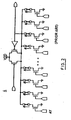
- FIG. 4 the layout of a section of an SDRAM implementing a column redundancy scheme according to a general embodiment of the present invention, is shown by numeral 60. More specifically, the column redundancy scheme illustrated is that for a 256M (Mbit) SDRAM in which the memory chip is divided into four banks, with 16x32 blocks per bank, i.e. 16 blocks of rowlines and 32 blocks of columns. Each bank is physically separated into two half banks in the column direction by row decoders, with each half bank having sixteen (16) column blocks. Each block comprises sixty four (64) normal columns 62 and one (1) redundant column.
- Mbit 16M
- Each bank is physically separated into two half banks in the column direction by row decoders, with each half bank having sixteen (16) column blocks.
- Each block comprises sixty four (64) normal columns 62 and one (1) redundant column.
- the section 60 shown has blocks numbered BLOCK1, BLOCK2, BLOCK3 and BLOCK4, and this layout is repeated four times for a half bank and eight times for an entire bank.
- the redundant column 64 associated with each block is shown at the right hand side thereof.
- Each block has a core Y decoder circuit YDEC 66 (Note: core circuitry refers to circuitry that is physically and functionally associated with the memory array; the terms column and Y are used interchangeably) and a single core redundant decoder RY 68 and driver RYDEC 70.
- the core Y decoders 66 are the second stage of the overall Y decoding for the chip.
- the core Y decoder gets its input from Y- predecoder (not shown) outputs PY and completes the column decoding.
- the first stage of column decoding is performed by the Y predecoders which, from global column address signals ACL[0:8] (not shown), generate the following predecoded Y addresses: PY0_1_ 2(7:0), Pry3_4(3:0), Pry5_6(3:0), PY7_8(3:0). All of these addresses are shown generally in Figure 4 as bus PY which carries the predecoded address signals to the core Y decoder 66 and core Y redundancy circuitry 68 and 70.
- Y address latch such as Y address latch, burst control, interleave control, sequential burst, interleave burst and Y address prefetch, all well-known in the SDRAM field, are all implemented in the Y predecoder circuit.
- each block has one Y redundancy column 64 and decoder RY 68 located at the side of the block.
- the Y redundancy decoder 68 and its corresponding BLOCK core Y decoder 66 share the same block selection signal (BSEL).
- BSEL block selection signal
- the core Y-decoders 66 and the redundant column 64 are clocked by a common Y select clock signal YSG.
- the overall structure of the four related redundant Y decoders, their relations to the core Y decoders and core-I/Os are illustrated in Figure 4 .
- the YSG signals are distributed locally.
- the YSG signal drivers at the center of the bank pass YSG signals throughout an entire bank.
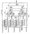
- Local YSG signal distribution circuitry indicated as YSG1, YSG2, YSG3 etc., and shown in detail in figure 9 , are provided for each block.
- Each of the local YSG signal distribution circuitry 72 switch and drive the YSG signal to either a normal core Y decoder 66 or to the corresponding Y redundancy decoder 68 in response to the output RDEC from the redundant Y decoder.
- the YSG signal distribution circuitry YSG1, YSG2, YSG3 etc.
- redundancy decoders within adjacent odd or even blocks are shared by all four blocks and can be used to replace any bad normal column within these four blocks.
- the DB_CTL outputs of the redundant Y decoder are connected to a four input AND gate 68b.
- the output RY10F4 from this gate is shared by the four redundancy decoders.
- DB_CTL When a redundant Y decoder is working, its output signal DB_CTL is set low, so RY10F4 is set low to inform the core-I/O circuitry (core data path circuitry) that a redundant Y decoder is being used.
- the BSEL signal goes high.
- the corresponding core-I/O needs to be enabled so core-I/O control signal DBSW_CTL goes high.
- the selected normal column is bad, it can be replaced by a redundant Y decoder, either within or outside the current block. Under this failure case even if BSEL is still high, whether DBSW_CTL goes high or not depends on the position of the failure replacement.
- the DBSW-CTL signal is responsible for switching the appropriate data bus pass gates 67 for coupling the selected column data to the data bus.
- the RY10F4 , BSEL and DB_CTL which controls the core I/O switch.
- the core-I/O switch rule is shown in the following table: INPUTS OUTPUT RY 10F4 BSEL DB_CTL DBSW_CTL 0 0 0 1 1 0 0 1 0 1 0 1 0 1 1 1 1 1 1
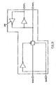
- FIG. 5(a) and 5(b) a schematic diagram of the core Y decoder 66a and a Y driver 66b.
- the combined circuit is shown schematically in block 66 of figure 4 .
- the core Y decoder 66a comprises a pair of NAND gates 72 and 74 for receiving the Y predecoder outputs PY0_1_2, PY3_4, PY5_6 and PY7_8.
- the outputs from the NAND gates 72 and 74 are combined in a NOR gate 76 to provide decoded output signal DEC.
- the decoder circuit 66a is equivalent to a four input AND gate.
- the output from the core Y decoder DEC is coupled to the column driver circuit 66b as shown in figure 5(b) .
- the normal or redundant column driver 66b receives the Y clock enable signals YSG_B0 and YSG_B1 at respective CMOS pass gates 82 and 84 which are controlled by the output signal DEC in conjunction with signals BUSL and BUSL.
- the clock signals YSG_B0 and YSG_B1 are passed through the CMOS gates at the appropriate time to an inverter 86 which then drives the corresponding column with the signal Y_B0 or Y_B1, depending on the state of the BUSL or the BUSL signals.
- the decoded signal DEC controls the pass gates 82 and 84.
- the overall core Y decoder YDEC 66 shown in figure 4 may be built with the two components shown in figures 5(a) and 5(b) .
- the Y address has nine bits, it then has 512 different decoding outputs.
- the even bits and odd bits may be separated to drive four even blocks and four odd blocks respectively.
- the arrangement will then repeat itself two times to realize a complete core wide decoder for a half bank or four times for a whole bank.
- each memory block has one redundant column located at the side of the block.
- the redundancy decoder RY and its corresponding core Y decoder YDEC share the same block selection signal (BSEL).
- the redundancy decoder RY shown in figure 6 includes a pair of address-compare circuits 92 and 94 which receive the predecoded addresses PY0_1_2, PY3_4, PY5_6 and PY7_8.
- Each address-compare circuit 92 and 94 is capable of being programmed with a single address thus the redundant Y decoder is capable of being programmed to two redundant addresses. Details of the address compare circuitry 92 and 94 will be discussed with reference to figure 7 .
- a row address signal AX12 is provided to the redundant Y decoder to perform the upper or lower column portion selection.
- the row address signal AX12 is coupled to the control inputs of a pair of CMOS pass gates 96 and 98 which receive the respective outputs from the address-compare circuits 92 and 94.
- the RY signal is coupled to an inverter 99 to drive the RDEC signal, which in turn drives the column driver 66b shown in figure 5(b) and the YSG signal distribution circuit 72 shown in figure 4 .
- the circuit also includes the INI1 and INI0 generation circuitry.
- the circuit comprises a chain of series connected inverters 100 driven from a main INI signal line, and the INI0 and INI1 signals taken as taps along the chain.
- the address compare circuits 92 and 94 of figure 6 are shown in detail. Since the predecoder ( figure 4 ) has four groups of predecoded outputs: PY0_1_ 2, PY3_4, PY5_6 and PY7_8, the address-compare circuit comprises four groups of programmable fuse circuits 142. Each group of fuse circuits includes four fuses with an associated fuse state evaluation circuit 180 shown in figure 8 . The inputs to each of the constituent fuse evaluation circuits in a group are derived from the predecoded column address signals in each group, i.e., PY0_1_2, PY3_4, PY5_6 or PY7_8.
- the outputs PY_OUT from each of the fuses in a group 142 are combined to provide respective signals PY_OUT1, PY_OUT2, PY_OUT3 and PY_OUT4. These signals are passed through an initialization circuit 144 before being combined in an address combiner circuit 146.
- the address combiner circuit is essentially a four input NAND gate which outputs a redundant select signal RY shown in figure 7 .
- the operation of the circuit 92 and 94 is as follows. If there are no defective columns and no need for redundancy, then no fuse circuits are blown, and the PY_OUT lines are all initialized to a logic low due to the initialization portion 144 of the circuit. This is in contrast with some of the prior art address-compare implementations where fuses of defective addresses were left intact while all fuses of non-defective columns were blown. That approach complicates the redundancy programming process considerably.
- the initialization circuit 144 is comprised of a pair of NOR gates 148 and 150, each connected to receive at its inputs a respective PY_OUT signal. Each of the NOR gate inputs are coupled to a respective NMOS transistor 152 and 154.
- the gates of these transistors are connected to their respective NOR gate output.
- the outputs of the NOR gates are logic high while the feedback connections via the feedback transistors further latch the inputs to logic low.
- the same logic low signals on lines PY_OUT are fed into NAND gates 155 and 156 thus producing logic highs at their outputs.
- the signal CST_BLK is a block redundancy test signal which is normally high, thus enabling NAND gates 157 and 158.
- both outputs from NAND gates 157 and 158 are logic low, which in turn produce a logic high out of NAND gate 160, indicating that redundancy is not being used, i.e., RY is logic high.
- the appropriate predecoder column address is programmed into each of the fuse circuit groups as described earlier.
- the programming signal lines PY_OUT1, PY_OUT2, PY_OUT3 and PY_OUT4 will all be set to logic high upon receipt of the predecoded signals since the address-compare circuit outputs will override the initialization devices; this process will be described in more detail below.
- the circuit 180 receives one of the predecoded address signals on its PY_IN terminal which is in turn connected to a CMOS pass gate 182 formed by a NMOS and PMOS transistor 183 and 184 respectively.
- the output of the CMOS pass gate 182 is the signal PY_OUT.
- the gates of pass gates 183 and 184 are controlled by a fuse element 186.
- the initial conditions for the pass gate 182 are set by a NAND gate 188, which in turn has its initial conditions determined by its inputs received from signals INI0 and INI1.
- the IN and INI1 signals are slightly delayed versions of one another with INI0 preceding INI1, as shown in figure 6 .
- a feedback PMOS transistor 190 has its gate connected to output of NAND gate 188 and its drain connected to one of the inputs 188b of the NAND gate 188, forming a half-latch.
- the feedback transistor 190 is used to latch the programmed redundancy address.
- the INI1 signal is applied directly to the other input 188a of the NAND gate 188 and to the gate of an NMOS transistor 192 having its source connected to one end of the fuse 186 the other end of which is connected to ground.
- the drain terminal of the NMOS transistor 192 is connected to the drain terminal of a PMOS transistor 194 which in turn has its source connected to the V DD supply.
- the INI0 signal is applied to the gate of the PMOS transistor 194.
- the common drain connection between the PMOS transistor 194 and the NMOS transistor 192 is connected to the first input 188b of the NAND gate 188.
- the output from the NAND gate 188 is connected via an inverter 196 to drive one of the pass gate transistors 183.
- the fuse state is evaluated as follows. Signal INI0 and INI1 are generated from the POWER_OK signal and INI1 is delayed from INI0. Initially, both INI0 and INI1 are low and the CMOS transmission gate is open and the predecoded signal cannot be passed. In general operation, if the fuse is not blown, once both INI0 and INI1 have become high, the CMOS transmission gate keeps its open state. On the other hand, if the fuse is blown, the CMOS transmission gate is closed and the predecoded signal PY_IN is passed as a redundant predecoded address signal PY_OUT.
- the feedback transistor 190 is used to latch the redundant state of the fuse circuit for the pass gate 182.
- this PMOS device 190 is fairly long to allow easy resetability of the half latch.
- long channel transistors tend to consume more power and take up more area than ones with shorter channels.
- the role of the delayed initialization signals INI0 and INI1 also serves to reduce the size of the feedback transistor 190 to a normal size. This implementation therefore reduces the current consumption during fuse evaluation.
- the delayed activation of the INI0 and INI1 signals avoids a race condition as follows: if INI0 and INI1 were one and the same signal, during the transition from a low to a high, both devices 194 and 192 would be conducting. Since device 194 could achieve a faster pull-up than the pull-down through 192 due to the resistance of the fuse, node 188b would tend to remain high, and once INI1 would be sufficiently high, both inputs to NAND gate 188 would be high, pulling its output low and turning on transistor 190. But while transistor 190 would be turning on, transistor 192 would also be turned on, creating a path from VDD to ground, assuming the fuse is not blown. The race is therefore between the turning on of 194,192 and 190.
- INI1 In contrast, by staggering the transition of INIO and INI1, where INI0 goes from low to high first and then after a delay, INI1 also goes from low to high, the following operation avoids the race condition mentioned above.
- INI0 initially low, device 194 is in the on state as power-up is occurring.
- INI0 goes from low to high, device 194 turns off and node 188b is left to float at high temporarily. Note that due to the fact that INI1 is still low, the output of 188 is still high, and device 190 is in an off state.
- INI1 begins its transition from low to high (no logic transitions can be instantaneous square-wave type transitions in actual operation, there will always be some slight delay resulting in more of a ramp-like transition), transistor 192 begins to turn on and node 188b is easily discharged since there is no contest with device 194.
- INI1 node 188a
- node 188b is going from floating high to low, and therefore, the output of NAND gate 188, as long as the fuse is not blown, will remain high, transistor 190 will not be turned on, and the pass gate 182 will remain off.
- the PY_IN signal will not be passed through the pass gate and the PY_OUT terminal signal will remain at its initialized state as described above.
- the switching circuit 72 ( figure 4 ) is shown in detail.
- the switching circuit includes a pair of YSG latches 200 coupled to latch and delay the input RDEC signal.
- the YSG signal is held for two clock cycles due to the dual data bus architecture.
- the output RYSG_B(1.0) and YSG_B(1.0) are coupled to the redundant driver 70 and the normal Y drivers respectively.
- RCTL (redundant decoder control) output from the latches 200 are coupled to an input of respective gates 202 and 204, while a CTL (decoder control) output is coupled to the inputs of a second pair of NAND gates 206 and 208.
- Both sets of NAND gates 202, 204 and 206, 208 receive the YSG signal on one of their other inputs.
- the YSG latches 200 have their outputs RCTL and CTL of complementary polarity.
- the NAND gates 202, 204 and 206, 208 are responsible for switching the YSG signal to either RYSG_B or YSG_B.
- the number of redundant Y drivers associated with a group of normal Y drivers may be varied.
- the column redundancy system may be applied to all types of RAMs such as DRAMs, SDRAMs, SGRAMs, and the like.
- the redundancy system described herein could also be adapted to implement row redundancy.
Landscapes
- Engineering & Computer Science (AREA)
- Theoretical Computer Science (AREA)
- Physics & Mathematics (AREA)
- General Engineering & Computer Science (AREA)
- General Physics & Mathematics (AREA)
- For Increasing The Reliability Of Semiconductor Memories (AREA)
- Dram (AREA)
- Logic Circuits (AREA)
- Techniques For Improving Reliability Of Storages (AREA)
Claims (18)
- Mémoire de semi-conducteur comprenant :une pluralité de blocs mémoire, chaque bloc mémoire ayant des éléments de mémoire agencés selon une pluralité de colonnes et une pluralité de lignes,la pluralité de colonnes dans chaque bloc mémoire comprenant une pluralité de colonnes normales (62) et au moins une colonne redondante (64),
chaque bloc mémoire comprenant en outreun circuit d'attaque de colonne normale (66) associé à chaque colonne normale, le circuit d'attaque de colonne normale étant adapté pour permettre l'accès à la colonne normale associée en réponse à un signal d'adresse de mémoire de colonne normale décodé,un décodeur (66) de colonne normale engendrant un signal d'adresse de mémoire de colonne normale décodé en réponse à un signal d'adresse de mémoire de colonne,un circuit d'attaque (70) de colonne redondante associé à chaque colonne redondante,le circuit d'attaque de colonne redondante étant adapté pour permettre l'accès à la colonne redondante associée en réponse à un signal d'adresse de mémoire de colonne redondante,un décodeur (68) de colonne redondante associé à chaque colonne redondante,chaque décodeur de colonne redondante comprenant au moins deux circuits comparateurs d'adresse (92, 94), pour comparer le signal d'adresse de mémoire de colonne à deux adresses de colonne mémorisées correspondant aux emplacements de deux colonnes défectueuses,un circuit d'acheminement de signaux d'adresse de ligne étant fourni à tous les décodeurs de colonne redondante, le niveau du signal d'adresse de ligne étant indicatif d'une partie supérieure ou inférieure d'une colonne,le signal d'adresse de ligne étant utilisé dans chaque décodeur de colonne redondante pour sélectionner la sortie de l'un des circuits de la paire de circuits comparateurs d'adresse, la sélection dépendant du niveau du signal d'adresse de ligne,le signal de sortie de sélection étant fourni- au circuit d'attaque de colonne redondante en tant que signal d'adresse de mémoire de colonne redondante,- à une porte (67) de passage de données du bloc mémoire pour connecter les données d'une colonne redondante activée de la colonne redondante sélectionnée à un bus de données commun. - Mémoire de semi-conducteur selon la revendication 1, dans laquelle le circuit d'attaque de colonne redondante dans un premier bloc mémoire est également sensible au signal de sortie de sélection, indicateur d'une colonne normale défectueuse dans un deuxième bloc mémoire.
- Mémoire de semi-conducteur selon la revendication 1 ou 2, dans laquelle un premier défaut dans une première colonne est remplacé par une première partie d'une première colonne redondante, et un deuxième défaut dans une deuxième colonne est remplacé par une deuxième partie de la première colonne redondante.
- Mémoire de semi-conducteur selon l'une quelconque des revendications 1 à 3, dans laquelle un premier défaut dans une partie supérieure d'une première colonne normale est remplacé par une partie supérieure d'une première colonne redondante, et un deuxième défaut dans une partie inférieure d'une deuxième colonne est remplacée par une partie inférieure de la première colonne redondante.
- Mémoire de semi-conducteur selon l'une quelconque des revendications 1 à 4, dans laquelle un premier défaut dans une partie supérieure d'une première colonne normale dans un premier bloc mémoire est remplacé par une partie supérieure d'une première colonne redondante, et un deuxième défaut dans une partie inférieure d'une deuxième colonne dans le premier bloc mémoire est remplacé par une partie inférieure de la première colonne redondante, la première colonne redondante étant située dans le premier bloc mémoire.
- Mémoire de semi-conducteur selon l'une quelconque des revendications 1 à 5, dans laquelle, pour chaque bloc, le signal d'adresse décodé est fourni par un décodeur d'adresse normal, et le signal de sortie de sélection, indicateur d'une colonne normale défectueuse, est fourni par un décodeur d'adresse redondant.
- Mémoire de semi-conducteur selon l'une quelconque des revendications 1 à 6, comprenant un circuit de fusible programmable pour mémoriser l'adresse colonne correspondant à l'emplacement de la colonne défectueuse.
- Mémoire de semi-conducteur selon l'une quelconque des revendications 1 à 7, comprenant, en outre, un circuit de commutation sensible au signal indicateur d'une correspondance, le circuit de commutation étant opérationnel pour connecter sélectivement un signal d'horloge au circuit d'attaque de colonne normale ou au circuit d'attaque de colonne redondante.
- Mémoire de semi-conducteur selon l'une quelconque des revendications 1 à 8, comprenant une porte de passage de données pour chaque colonne redondante, la porte de passage de données étant sensible à un signal de commande de chemin de données, pour passer les données depuis une colonne redondante activée à un bus de données commun.
- Mémoire de semi-conducteur selon l'une quelconque des revendications 1 à 9, dans laquelle l'accès à la pluralité de blocs mémoire est activé par la réalisation d'un signal de sélection de bloc.
- Procédé de remplacement d'une colonne défectueuse dans un bloc mémoire, le bloc mémoire étant l'un d'une pluralité de blocs mémoire dans une mémoire de semi-conducteur ayant des cellules de mémoire agencées en lignes et colonnes, chaque bloc mémoire ayant une pluralité de colonnes normales (62) et au moins une colonne redondante (64), le procédé comprenant les étapes consistant à :programmer chaque décodeur (68) de colonne redondante, comprenant au moins deux circuits (92, 94) comparateurs d'adresse pour comparer le signal d'adresse de mémoire de colonne à deux adresses de colonne mémorisées correspondant aux emplacements de deux colonnes défectueuses,fournir un signal d'adresse de ligne à bit unique à tous les décodeurs de colonne redondante, le niveau du signal d'adresse de ligne indiquant une partie supérieure ou une partie inférieure d'une colonne,utiliser le signal d'adresse de ligne dans chaque décodeur de colonne redondante pour sélectionner la sortie de l'un des circuits de la paire de circuits comparateurs d'adresse, la sélection dépendant du niveau du signal d'adresse de ligne,fournir le signal de sortie de sélection- au circuit d'attaque de colonne redondante en tant que signal d'adresse de mémoire de colonne redondante,- à une porte de passage de données (67) du bloc mémoire, pour connecter les données de colonne redondante sélectionnée depuis une colonne redondante active à un bus de données commun.
- Procédé selon la revendication 11, dans lequel le signal d'adresse de ligne indique une colonne normale, pour laquelle l'accès se fait dans l'un de la pluralité de blocs mémoire.
- Procédé selon la revendication 11 ou 12, dans lequel la programmation d'une adresse de colonne comprend l'étape consistant à faire sauter une pluralité de fusibles correspondant à l'adresse de colonne de la colonne défectueuse.
- Procédé selon l'une quelconque des revendications 11 à 13, comprenant l'étape consistant à activer l'accès à la pluralité de blocs mémoire en réalisant un signal de sélection de bloc.
- Procédé selon l'une quelconque des revendications 11 à 14, comprenant l'étape consistant à remplacer un premier défaut dans une première colonne par une première partie d'une première colonne redondante, et à remplacer un deuxième défaut dans une deuxième colonne par une deuxième partie de la première colonne redondante.
- Procédé selon l'une quelconque des revendications 11 à 15, comprenant l'étape consistant à remplacer un premier défaut dans une partie supérieure d'une première colonne normale par une partie supérieure d'une première colonne redondante, et à remplacer un deuxième défaut dans une partie inférieure d'une deuxième colonne par une partie inférieure de la première colonne redondante.
- Procédé selon l'une quelconque des revendications 11 à 16, comprenant l'étape consistant à remplacer un premier défaut dans une partie supérieure d'une première colonne normale dans un premier bloc mémoire part une partie supérieure d'une première colonne redondante, et à remplacer un deuxième défaut dans une partie inférieure d'une deuxième colonne dans le premier bloc mémoire par une partie inférieure de la première colonne redondante, la première colonne redondante étant située dans le premier bloc mémoire.
- Procédé selon l'une quelconque des revendications 11 à 16, comprenant, en outre, l'étape consistant à connecter sélectivement un signal d'horloge au circuit d'attaque de colonne normale ou au circuit d'attaque de colonne redondante.
Applications Claiming Priority (3)
| Application Number | Priority Date | Filing Date | Title |
|---|---|---|---|
| US09/182,495 US6137735A (en) | 1998-10-30 | 1998-10-30 | Column redundancy circuit with reduced signal path delay |
| US182495 | 1998-10-30 | ||
| EP99953491A EP1125203B1 (fr) | 1998-10-30 | 1999-10-29 | Circuit de redondance de colonnes a decalage reduit du trajet du signal |
Related Parent Applications (1)
| Application Number | Title | Priority Date | Filing Date |
|---|---|---|---|
| EP99953491A Division EP1125203B1 (fr) | 1998-10-30 | 1999-10-29 | Circuit de redondance de colonnes a decalage reduit du trajet du signal |
Publications (4)
| Publication Number | Publication Date |
|---|---|
| EP1526458A2 EP1526458A2 (fr) | 2005-04-27 |
| EP1526458A3 EP1526458A3 (fr) | 2006-03-29 |
| EP1526458B1 true EP1526458B1 (fr) | 2008-10-08 |
| EP1526458B8 EP1526458B8 (fr) | 2008-12-24 |
Family
ID=22668727
Family Applications (2)
| Application Number | Title | Priority Date | Filing Date |
|---|---|---|---|
| EP04023097A Expired - Lifetime EP1526458B8 (fr) | 1998-10-30 | 1999-10-29 | Circuit de redondance de colonne à décalage réduit du trajet du signal |
| EP99953491A Expired - Lifetime EP1125203B1 (fr) | 1998-10-30 | 1999-10-29 | Circuit de redondance de colonnes a decalage reduit du trajet du signal |
Family Applications After (1)
| Application Number | Title | Priority Date | Filing Date |
|---|---|---|---|
| EP99953491A Expired - Lifetime EP1125203B1 (fr) | 1998-10-30 | 1999-10-29 | Circuit de redondance de colonnes a decalage reduit du trajet du signal |
Country Status (10)
| Country | Link |
|---|---|
| US (1) | US6137735A (fr) |
| EP (2) | EP1526458B8 (fr) |
| JP (1) | JP4965025B2 (fr) |
| KR (1) | KR100724816B1 (fr) |
| CN (1) | CN1186725C (fr) |
| AT (1) | ATE278217T1 (fr) |
| AU (1) | AU1024500A (fr) |
| CA (1) | CA2347765C (fr) |
| DE (2) | DE69920735T2 (fr) |
| WO (1) | WO2000026784A1 (fr) |
Families Citing this family (10)
| Publication number | Priority date | Publication date | Assignee | Title |
|---|---|---|---|---|
| KR100363085B1 (ko) * | 1999-11-05 | 2002-12-05 | 삼성전자 주식회사 | 리던던시 효율을 향상시키는 로우 리던던시 스킴을 갖는반도체장치 |
| JP2002050191A (ja) * | 2000-08-02 | 2002-02-15 | Fujitsu Ltd | 半導体記憶装置 |
| US6775759B2 (en) * | 2001-12-07 | 2004-08-10 | Micron Technology, Inc. | Sequential nibble burst ordering for data |
| US20040015645A1 (en) * | 2002-07-19 | 2004-01-22 | Dodd James M. | System, apparatus, and method for a flexible DRAM architecture |
| US6674673B1 (en) | 2002-08-26 | 2004-01-06 | International Business Machines Corporation | Column redundancy system and method for a micro-cell embedded DRAM (e-DRAM) architecture |
| JP4467565B2 (ja) * | 2004-02-20 | 2010-05-26 | スパンション エルエルシー | 半導体記憶装置および半導体記憶装置の制御方法 |
| US7035152B1 (en) * | 2004-10-14 | 2006-04-25 | Micron Technology, Inc. | System and method for redundancy memory decoding |
| US7251173B2 (en) * | 2005-08-02 | 2007-07-31 | Micron Technology, Inc. | Combination column redundancy system for a memory array |
| CN105355233B (zh) * | 2015-11-23 | 2018-04-10 | 清华大学 | 基于pcm反转纠错算法的高效数据写入方法 |
| CN107389211B (zh) * | 2017-06-29 | 2019-03-12 | 西安邮电大学 | 一种二进制码转温度计码电路 |
Family Cites Families (17)
| Publication number | Priority date | Publication date | Assignee | Title |
|---|---|---|---|---|
| US4598388A (en) * | 1985-01-22 | 1986-07-01 | Texas Instruments Incorporated | Semiconductor memory with redundant column circuitry |
| JP2564507B2 (ja) * | 1985-04-16 | 1996-12-18 | 富士通株式会社 | 半導体記憶装置 |
| JPH01125799A (ja) * | 1987-11-11 | 1989-05-18 | Fujitsu Ltd | 半導体記憶装置 |
| US5270975A (en) * | 1990-03-29 | 1993-12-14 | Texas Instruments Incorporated | Memory device having a non-uniform redundancy decoder arrangement |
| EP1227504B1 (fr) * | 1991-08-28 | 2004-08-04 | Oki Electric Industry Co., Ltd. | Dispositif de mémoire à semiconducteurs |
| US5257229A (en) * | 1992-01-31 | 1993-10-26 | Sgs-Thomson Microelectronics, Inc. | Column redundancy architecture for a read/write memory |
| US5268866A (en) * | 1992-03-02 | 1993-12-07 | Motorola, Inc. | Memory with column redundancy and localized column redundancy control signals |
| ATE187826T1 (de) * | 1994-08-12 | 2000-01-15 | Siemens Ag | Redundanz-schaltungsanordnung für einen integrierten halbleiterspeicher |
| KR0130030B1 (ko) * | 1994-08-25 | 1998-10-01 | 김광호 | 반도체 메모리 장치의 컬럼 리던던시 회로 및 그 방법 |
| US5572470A (en) * | 1995-05-10 | 1996-11-05 | Sgs-Thomson Microelectronics, Inc. | Apparatus and method for mapping a redundant memory column to a defective memory column |
| JPH0955080A (ja) * | 1995-08-08 | 1997-02-25 | Fujitsu Ltd | 半導体記憶装置及び半導体記憶装置のセル情報の書き込み及び読み出し方法 |
| ATE220228T1 (de) * | 1995-08-09 | 2002-07-15 | Infineon Technologies Ag | Integrierte halbleiter-speichervorrichtung mit redundanzschaltungsanordnung |
| US5646896A (en) * | 1995-10-31 | 1997-07-08 | Hyundai Electronics America | Memory device with reduced number of fuses |
| US5732030A (en) * | 1996-06-25 | 1998-03-24 | Texas Instruments Incorporated | Method and system for reduced column redundancy using a dual column select |
| JPH10275493A (ja) * | 1997-03-31 | 1998-10-13 | Nec Corp | 半導体記憶装置 |
| CA2202692C (fr) * | 1997-04-14 | 2006-06-13 | Mosaid Technologies Incorporated | Redondance de colonne dans des memoires semi-conductrices |
| KR100281284B1 (ko) * | 1998-06-29 | 2001-02-01 | 김영환 | 컬럼 리던던시 회로 |
-
1998
- 1998-10-30 US US09/182,495 patent/US6137735A/en not_active Expired - Lifetime
-
1999
- 1999-10-29 AU AU10245/00A patent/AU1024500A/en not_active Abandoned
- 1999-10-29 CN CNB998128104A patent/CN1186725C/zh not_active Expired - Lifetime
- 1999-10-29 CA CA002347765A patent/CA2347765C/fr not_active Expired - Fee Related
- 1999-10-29 EP EP04023097A patent/EP1526458B8/fr not_active Expired - Lifetime
- 1999-10-29 DE DE69920735T patent/DE69920735T2/de not_active Expired - Lifetime
- 1999-10-29 WO PCT/CA1999/001054 patent/WO2000026784A1/fr not_active Ceased
- 1999-10-29 EP EP99953491A patent/EP1125203B1/fr not_active Expired - Lifetime
- 1999-10-29 AT AT99953491T patent/ATE278217T1/de not_active IP Right Cessation
- 1999-10-29 DE DE69939716T patent/DE69939716D1/de not_active Expired - Lifetime
- 1999-10-29 KR KR1020017005435A patent/KR100724816B1/ko not_active Expired - Fee Related
- 1999-10-29 JP JP2000580093A patent/JP4965025B2/ja not_active Expired - Fee Related
Also Published As
| Publication number | Publication date |
|---|---|
| JP4965025B2 (ja) | 2012-07-04 |
| ATE278217T1 (de) | 2004-10-15 |
| DE69920735T2 (de) | 2005-02-10 |
| EP1125203B1 (fr) | 2004-09-29 |
| EP1526458B8 (fr) | 2008-12-24 |
| CN1331818A (zh) | 2002-01-16 |
| EP1526458A3 (fr) | 2006-03-29 |
| DE69920735D1 (de) | 2004-11-04 |
| CA2347765A1 (fr) | 2000-05-11 |
| WO2000026784A1 (fr) | 2000-05-11 |
| KR100724816B1 (ko) | 2007-06-04 |
| CA2347765C (fr) | 2008-07-29 |
| JP2002529874A (ja) | 2002-09-10 |
| CN1186725C (zh) | 2005-01-26 |
| EP1526458A2 (fr) | 2005-04-27 |
| DE69939716D1 (de) | 2008-11-20 |
| AU1024500A (en) | 2000-05-22 |
| US6137735A (en) | 2000-10-24 |
| EP1125203A1 (fr) | 2001-08-22 |
| KR20010085983A (ko) | 2001-09-07 |
Similar Documents
| Publication | Publication Date | Title |
|---|---|---|
| US6084818A (en) | Semiconductor memory device capable of efficient memory cell select operation with reduced element count | |
| CA2389986C (fr) | Architecture a mise en oeuvre de redondance multi-instance | |
| KR100790442B1 (ko) | 글로벌 리던던시를 갖는 메모리소자 및 그 동작 방법 | |
| US6272056B1 (en) | Semiconductor memory device capable of implementing redundancy-based repair efficiently in relation to layout and operating speed and semiconductor integrated circuit device having such semiconductor memory device | |
| US5796662A (en) | Integrated circuit chip with a wide I/O memory array and redundant data lines | |
| US20020024859A1 (en) | Semiconductor memory device having a large band width and allowing efficient execution of redundant repair | |
| EP0847010B1 (fr) | Architecture à blocs avec redondance de ligne | |
| US5963489A (en) | Method and apparatus for redundancy word line replacement in a repairable semiconductor memory device | |
| US6144591A (en) | Redundancy selection circuit for semiconductor memories | |
| CA2202692C (fr) | Redondance de colonne dans des memoires semi-conductrices | |
| EP1526458B1 (fr) | Circuit de redondance de colonne à décalage réduit du trajet du signal | |
| US5978291A (en) | Sub-block redundancy replacement for a giga-bit scale DRAM | |
| US6058052A (en) | Redundancy scheme providing improvements in redundant circuit access time and integrated circuit layout area | |
| US6335897B1 (en) | Semiconductor memory device including redundancy circuit adopting latch cell | |
| US5757716A (en) | Integrated circuit memory devices and methods including programmable block disabling and programmable block selection | |
| US12548615B2 (en) | Apparatuses and methods for repairing multiple bit lines with a same column select value | |
| US20020196684A1 (en) | Semiconductor memory device and method of repairing the same | |
| US7116591B2 (en) | Redundancy circuits and memory devices having a twist bitline scheme and methods of repairing defective cells in the same | |
| US6928008B2 (en) | Semiconductor memory devices with data line redundancy schemes and method therefore | |
| KR0172352B1 (ko) | 반도체 메모리 장치의 컬럼 리던던시 제어회로 | |
| CA2246763C (fr) | Circuit ameliore de selection de redondance pour memoires a semiconducteurs | |
| JP2002050192A (ja) | 半導体装置 |
Legal Events
| Date | Code | Title | Description |
|---|---|---|---|
| PUAI | Public reference made under article 153(3) epc to a published international application that has entered the european phase |
Free format text: ORIGINAL CODE: 0009012 |
|
| AC | Divisional application: reference to earlier application |
Ref document number: 1125203 Country of ref document: EP Kind code of ref document: P |
|
| AK | Designated contracting states |
Kind code of ref document: A2 Designated state(s): AT BE CH CY DE DK ES FI FR GB GR IE IT LI LU MC NL PT SE |
|
| PUAL | Search report despatched |
Free format text: ORIGINAL CODE: 0009013 |
|
| AK | Designated contracting states |
Kind code of ref document: A3 Designated state(s): AT BE CH CY DE DK ES FI FR GB GR IE IT LI LU MC NL PT SE |
|
| RIC1 | Information provided on ipc code assigned before grant |
Ipc: G11C 29/00 20060101AFI20060203BHEP |
|
| 17P | Request for examination filed |
Effective date: 20060920 |
|
| 17Q | First examination report despatched |
Effective date: 20061016 |
|
| AKX | Designation fees paid |
Designated state(s): DE FI FR GB IT NL |
|
| GRAP | Despatch of communication of intention to grant a patent |
Free format text: ORIGINAL CODE: EPIDOSNIGR1 |
|
| GRAS | Grant fee paid |
Free format text: ORIGINAL CODE: EPIDOSNIGR3 |
|
| GRAA | (expected) grant |
Free format text: ORIGINAL CODE: 0009210 |
|
| AC | Divisional application: reference to earlier application |
Ref document number: 1125203 Country of ref document: EP Kind code of ref document: P |
|
| AK | Designated contracting states |
Kind code of ref document: B1 Designated state(s): DE FI FR GB IT NL |
|
| REG | Reference to a national code |
Ref country code: GB Ref legal event code: FG4D |
|
| RAP2 | Party data changed (patent owner data changed or rights of a patent transferred) |
Owner name: MOSAID TECHNOLOGIES INCORPORATED Owner name: PANASONIC CORPORATION |
|
| REF | Corresponds to: |
Ref document number: 69939716 Country of ref document: DE Date of ref document: 20081120 Kind code of ref document: P |
|
| NLT2 | Nl: modifications (of names), taken from the european patent patent bulletin |
Owner name: MOSAID TECHNOLOGIES INCORPORATED EN PANASONIC CORP Effective date: 20081119 |
|
| PLBE | No opposition filed within time limit |
Free format text: ORIGINAL CODE: 0009261 |
|
| STAA | Information on the status of an ep patent application or granted ep patent |
Free format text: STATUS: NO OPPOSITION FILED WITHIN TIME LIMIT |
|
| PG25 | Lapsed in a contracting state [announced via postgrant information from national office to epo] |
Ref country code: IT Free format text: LAPSE BECAUSE OF FAILURE TO SUBMIT A TRANSLATION OF THE DESCRIPTION OR TO PAY THE FEE WITHIN THE PRESCRIBED TIME-LIMIT Effective date: 20081008 |
|
| 26N | No opposition filed |
Effective date: 20090709 |
|
| REG | Reference to a national code |
Ref country code: FR Ref legal event code: CA |
|
| REG | Reference to a national code |
Ref country code: DE Ref legal event code: R082 Ref document number: 69939716 Country of ref document: DE Representative=s name: 24IP LAW GROUP SONNENBERG FORTMANN, DE |
|
| REG | Reference to a national code |
Ref country code: FR Ref legal event code: CA Effective date: 20141021 Ref country code: FR Ref legal event code: CD Owner name: CONVERSANT INTELLECTUAL PROPERTY MANAGEMENT IN, CA Effective date: 20141021 |
|
| REG | Reference to a national code |
Ref country code: DE Ref legal event code: R081 Ref document number: 69939716 Country of ref document: DE Owner name: PANASONIC CORPORATION, KADOMA-SHI, JP Free format text: FORMER OWNER: MOSAID TECHNOLOGIES INC., PANASONIC CORPORATION, , JP Effective date: 20141120 Ref country code: DE Ref legal event code: R082 Ref document number: 69939716 Country of ref document: DE Representative=s name: 24IP LAW GROUP SONNENBERG FORTMANN, DE Effective date: 20141120 Ref country code: DE Ref legal event code: R081 Ref document number: 69939716 Country of ref document: DE Owner name: CONVERSANT INTELLECTUAL PROPERTY MANAGEMENT IN, CA Free format text: FORMER OWNER: MOSAID TECHNOLOGIES INC., PANASONIC CORPORATION, , JP Effective date: 20141120 Ref country code: DE Ref legal event code: R081 Ref document number: 69939716 Country of ref document: DE Owner name: PANASONIC CORPORATION, KADOMA-SHI, JP Free format text: FORMER OWNERS: MOSAID TECHNOLOGIES INC., OTTAWA, ONTARIO, CA; PANASONIC CORPORATION, KADOMA-SHI, OSAKA, JP Effective date: 20141120 Ref country code: DE Ref legal event code: R081 Ref document number: 69939716 Country of ref document: DE Owner name: CONVERSANT INTELLECTUAL PROPERTY MANAGEMENT IN, CA Free format text: FORMER OWNERS: MOSAID TECHNOLOGIES INC., OTTAWA, ONTARIO, CA; PANASONIC CORPORATION, KADOMA-SHI, OSAKA, JP Effective date: 20141120 |
|
| REG | Reference to a national code |
Ref country code: NL Ref legal event code: TD Effective date: 20150216 |
|
| REG | Reference to a national code |
Ref country code: FR Ref legal event code: PLFP Year of fee payment: 17 |
|
| PGFP | Annual fee paid to national office [announced via postgrant information from national office to epo] |
Ref country code: GB Payment date: 20151019 Year of fee payment: 17 Ref country code: FI Payment date: 20151020 Year of fee payment: 17 |
|
| PGFP | Annual fee paid to national office [announced via postgrant information from national office to epo] |
Ref country code: FR Payment date: 20151029 Year of fee payment: 17 Ref country code: NL Payment date: 20151029 Year of fee payment: 17 |
|
| PGFP | Annual fee paid to national office [announced via postgrant information from national office to epo] |
Ref country code: DE Payment date: 20161214 Year of fee payment: 18 |
|
| REG | Reference to a national code |
Ref country code: NL Ref legal event code: MM Effective date: 20161101 |
|
| GBPC | Gb: european patent ceased through non-payment of renewal fee |
Effective date: 20161029 |
|
| REG | Reference to a national code |
Ref country code: FR Ref legal event code: ST Effective date: 20170630 |
|
| PG25 | Lapsed in a contracting state [announced via postgrant information from national office to epo] |
Ref country code: FI Free format text: LAPSE BECAUSE OF NON-PAYMENT OF DUE FEES Effective date: 20161029 Ref country code: FR Free format text: LAPSE BECAUSE OF NON-PAYMENT OF DUE FEES Effective date: 20161102 Ref country code: GB Free format text: LAPSE BECAUSE OF NON-PAYMENT OF DUE FEES Effective date: 20161029 |
|
| PG25 | Lapsed in a contracting state [announced via postgrant information from national office to epo] |
Ref country code: NL Free format text: LAPSE BECAUSE OF NON-PAYMENT OF DUE FEES Effective date: 20161101 |
|
| REG | Reference to a national code |
Ref country code: DE Ref legal event code: R119 Ref document number: 69939716 Country of ref document: DE |
|
| PG25 | Lapsed in a contracting state [announced via postgrant information from national office to epo] |
Ref country code: DE Free format text: LAPSE BECAUSE OF NON-PAYMENT OF DUE FEES Effective date: 20180501 |