EP1524645B1 - Verfahren und Vorrichtung zur Ansteuerung eines Plasma-Anzeigefeldes - Google Patents
Verfahren und Vorrichtung zur Ansteuerung eines Plasma-Anzeigefeldes Download PDFInfo
- Publication number
- EP1524645B1 EP1524645B1 EP04256288A EP04256288A EP1524645B1 EP 1524645 B1 EP1524645 B1 EP 1524645B1 EP 04256288 A EP04256288 A EP 04256288A EP 04256288 A EP04256288 A EP 04256288A EP 1524645 B1 EP1524645 B1 EP 1524645B1
- Authority
- EP
- European Patent Office
- Prior art keywords
- temperature
- subfield
- panel
- mapping
- dielectric layer
- Prior art date
- Legal status (The legal status is an assumption and is not a legal conclusion. Google has not performed a legal analysis and makes no representation as to the accuracy of the status listed.)
- Expired - Lifetime
Links
- 238000000034 method Methods 0.000 title claims abstract description 28
- 238000013507 mapping Methods 0.000 claims abstract description 41
- 239000000758 substrate Substances 0.000 claims abstract description 21
- 230000004888 barrier function Effects 0.000 claims abstract description 10
- 229910052751 metal Inorganic materials 0.000 claims abstract description 9
- 239000002184 metal Substances 0.000 claims abstract description 9
- 238000010586 diagram Methods 0.000 description 9
- 239000007789 gas Substances 0.000 description 7
- 239000002245 particle Substances 0.000 description 6
- 238000012937 correction Methods 0.000 description 5
- 230000037452 priming Effects 0.000 description 4
- 238000009792 diffusion process Methods 0.000 description 3
- 230000033001 locomotion Effects 0.000 description 3
- 238000004544 sputter deposition Methods 0.000 description 2
- 238000011161 development Methods 0.000 description 1
- 230000018109 developmental process Effects 0.000 description 1
- 238000007599 discharging Methods 0.000 description 1
- 238000005516 engineering process Methods 0.000 description 1
- AMGQUBHHOARCQH-UHFFFAOYSA-N indium;oxotin Chemical compound [In].[Sn]=O AMGQUBHHOARCQH-UHFFFAOYSA-N 0.000 description 1
- 239000011261 inert gas Substances 0.000 description 1
- 230000010354 integration Effects 0.000 description 1
- 238000004519 manufacturing process Methods 0.000 description 1
- 238000012986 modification Methods 0.000 description 1
- 230000004048 modification Effects 0.000 description 1
- 238000005192 partition Methods 0.000 description 1
- 230000002093 peripheral effect Effects 0.000 description 1
- 238000013139 quantization Methods 0.000 description 1
- 230000004044 response Effects 0.000 description 1
- 239000000126 substance Substances 0.000 description 1
- 230000000007 visual effect Effects 0.000 description 1
Images
Classifications
-
- G—PHYSICS
- G09—EDUCATION; CRYPTOGRAPHY; DISPLAY; ADVERTISING; SEALS
- G09G—ARRANGEMENTS OR CIRCUITS FOR CONTROL OF INDICATING DEVICES USING STATIC MEANS TO PRESENT VARIABLE INFORMATION
- G09G3/00—Control arrangements or circuits, of interest only in connection with visual indicators other than cathode-ray tubes
- G09G3/20—Control arrangements or circuits, of interest only in connection with visual indicators other than cathode-ray tubes for presentation of an assembly of a number of characters, e.g. a page, by composing the assembly by combination of individual elements arranged in a matrix no fixed position being assigned to or needed to be assigned to the individual characters or partial characters
- G09G3/22—Control arrangements or circuits, of interest only in connection with visual indicators other than cathode-ray tubes for presentation of an assembly of a number of characters, e.g. a page, by composing the assembly by combination of individual elements arranged in a matrix no fixed position being assigned to or needed to be assigned to the individual characters or partial characters using controlled light sources
- G09G3/28—Control arrangements or circuits, of interest only in connection with visual indicators other than cathode-ray tubes for presentation of an assembly of a number of characters, e.g. a page, by composing the assembly by combination of individual elements arranged in a matrix no fixed position being assigned to or needed to be assigned to the individual characters or partial characters using controlled light sources using luminous gas-discharge panels, e.g. plasma panels
- G09G3/288—Control arrangements or circuits, of interest only in connection with visual indicators other than cathode-ray tubes for presentation of an assembly of a number of characters, e.g. a page, by composing the assembly by combination of individual elements arranged in a matrix no fixed position being assigned to or needed to be assigned to the individual characters or partial characters using controlled light sources using luminous gas-discharge panels, e.g. plasma panels using AC panels
- G09G3/291—Control arrangements or circuits, of interest only in connection with visual indicators other than cathode-ray tubes for presentation of an assembly of a number of characters, e.g. a page, by composing the assembly by combination of individual elements arranged in a matrix no fixed position being assigned to or needed to be assigned to the individual characters or partial characters using controlled light sources using luminous gas-discharge panels, e.g. plasma panels using AC panels controlling the gas discharge to control a cell condition, e.g. by means of specific pulse shapes
-
- G—PHYSICS
- G09—EDUCATION; CRYPTOGRAPHY; DISPLAY; ADVERTISING; SEALS
- G09G—ARRANGEMENTS OR CIRCUITS FOR CONTROL OF INDICATING DEVICES USING STATIC MEANS TO PRESENT VARIABLE INFORMATION
- G09G3/00—Control arrangements or circuits, of interest only in connection with visual indicators other than cathode-ray tubes
- G09G3/20—Control arrangements or circuits, of interest only in connection with visual indicators other than cathode-ray tubes for presentation of an assembly of a number of characters, e.g. a page, by composing the assembly by combination of individual elements arranged in a matrix no fixed position being assigned to or needed to be assigned to the individual characters or partial characters
- G09G3/2007—Display of intermediate tones
- G09G3/2018—Display of intermediate tones by time modulation using two or more time intervals
- G09G3/2022—Display of intermediate tones by time modulation using two or more time intervals using sub-frames
-
- G—PHYSICS
- G09—EDUCATION; CRYPTOGRAPHY; DISPLAY; ADVERTISING; SEALS
- G09G—ARRANGEMENTS OR CIRCUITS FOR CONTROL OF INDICATING DEVICES USING STATIC MEANS TO PRESENT VARIABLE INFORMATION
- G09G3/00—Control arrangements or circuits, of interest only in connection with visual indicators other than cathode-ray tubes
- G09G3/20—Control arrangements or circuits, of interest only in connection with visual indicators other than cathode-ray tubes for presentation of an assembly of a number of characters, e.g. a page, by composing the assembly by combination of individual elements arranged in a matrix no fixed position being assigned to or needed to be assigned to the individual characters or partial characters
- G09G3/22—Control arrangements or circuits, of interest only in connection with visual indicators other than cathode-ray tubes for presentation of an assembly of a number of characters, e.g. a page, by composing the assembly by combination of individual elements arranged in a matrix no fixed position being assigned to or needed to be assigned to the individual characters or partial characters using controlled light sources
- G09G3/28—Control arrangements or circuits, of interest only in connection with visual indicators other than cathode-ray tubes for presentation of an assembly of a number of characters, e.g. a page, by composing the assembly by combination of individual elements arranged in a matrix no fixed position being assigned to or needed to be assigned to the individual characters or partial characters using controlled light sources using luminous gas-discharge panels, e.g. plasma panels
- G09G3/2803—Display of gradations
-
- G—PHYSICS
- G09—EDUCATION; CRYPTOGRAPHY; DISPLAY; ADVERTISING; SEALS
- G09G—ARRANGEMENTS OR CIRCUITS FOR CONTROL OF INDICATING DEVICES USING STATIC MEANS TO PRESENT VARIABLE INFORMATION
- G09G3/00—Control arrangements or circuits, of interest only in connection with visual indicators other than cathode-ray tubes
- G09G3/20—Control arrangements or circuits, of interest only in connection with visual indicators other than cathode-ray tubes for presentation of an assembly of a number of characters, e.g. a page, by composing the assembly by combination of individual elements arranged in a matrix no fixed position being assigned to or needed to be assigned to the individual characters or partial characters
- G09G3/22—Control arrangements or circuits, of interest only in connection with visual indicators other than cathode-ray tubes for presentation of an assembly of a number of characters, e.g. a page, by composing the assembly by combination of individual elements arranged in a matrix no fixed position being assigned to or needed to be assigned to the individual characters or partial characters using controlled light sources
- G09G3/28—Control arrangements or circuits, of interest only in connection with visual indicators other than cathode-ray tubes for presentation of an assembly of a number of characters, e.g. a page, by composing the assembly by combination of individual elements arranged in a matrix no fixed position being assigned to or needed to be assigned to the individual characters or partial characters using controlled light sources using luminous gas-discharge panels, e.g. plasma panels
- G09G3/288—Control arrangements or circuits, of interest only in connection with visual indicators other than cathode-ray tubes for presentation of an assembly of a number of characters, e.g. a page, by composing the assembly by combination of individual elements arranged in a matrix no fixed position being assigned to or needed to be assigned to the individual characters or partial characters using controlled light sources using luminous gas-discharge panels, e.g. plasma panels using AC panels
- G09G3/296—Driving circuits for producing the waveforms applied to the driving electrodes
-
- G—PHYSICS
- G09—EDUCATION; CRYPTOGRAPHY; DISPLAY; ADVERTISING; SEALS
- G09G—ARRANGEMENTS OR CIRCUITS FOR CONTROL OF INDICATING DEVICES USING STATIC MEANS TO PRESENT VARIABLE INFORMATION
- G09G2320/00—Control of display operating conditions
- G09G2320/02—Improving the quality of display appearance
- G09G2320/0247—Flicker reduction other than flicker reduction circuits used for single beam cathode-ray tubes
-
- G—PHYSICS
- G09—EDUCATION; CRYPTOGRAPHY; DISPLAY; ADVERTISING; SEALS
- G09G—ARRANGEMENTS OR CIRCUITS FOR CONTROL OF INDICATING DEVICES USING STATIC MEANS TO PRESENT VARIABLE INFORMATION
- G09G2320/00—Control of display operating conditions
- G09G2320/02—Improving the quality of display appearance
- G09G2320/0266—Reduction of sub-frame artefacts
-
- G—PHYSICS
- G09—EDUCATION; CRYPTOGRAPHY; DISPLAY; ADVERTISING; SEALS
- G09G—ARRANGEMENTS OR CIRCUITS FOR CONTROL OF INDICATING DEVICES USING STATIC MEANS TO PRESENT VARIABLE INFORMATION
- G09G2320/00—Control of display operating conditions
- G09G2320/04—Maintaining the quality of display appearance
- G09G2320/041—Temperature compensation
Definitions
- the present invention relates to a plasma display panel, and more particularly, to a method and an apparatus of driving a plasma display panel.
- PDPs plasma display panels
- a mixed gas such as (He + Xe), (Ne + Xe), or (He + Ne + Xe).
- PDPs provide excellent quality of image due to recent developments in technology, as well as permitting manufacture in slim sizes and wide-screen configurations.
- a 3-electrode AC surface discharge type PDP lowers the voltage necessary to achieve electric discharge using wall charges accumulated on a surface and protects the electrodes from sputtering that occurs on the electric discharge, thereby being advantageous in enabling low voltage driving and long endurance.
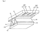
- FIG. 1 is a perspective diagram of a discharge cell of a 3-electrode AC surface discharge type PDP according to the related art.
- a discharge cell of a 3-electrodes AC surface discharge type PDP consists of a scan electrode 30Y and sustain electrode 30Z formed on an upper substrate 10 and an address electrode 20X formed on a lower substrate 18.
- Each of the scan and sustain electrodes 30Y and 30Z has a line width smaller than that of a transparent electrode 12Y or 12Z and includes a metal bus electrode 13Y or 13Z.
- the transparent electrodes 12Y and 12Z are generally formed of indium tin oxide (ITO) on the upper substrate 10.
- the metal bus electrodes 13Y and 13Z are generally formed of metal such as Cr or the like on the transparent electrodes 12Y and 12Z to reduce the voltage drops caused by the high resistance of the transparent electrodes 12Y and 12Z , respectively.
- An upper dielectric layer 14 and protecting layer 16 are stacked over the upper substrate 10 including the scan and sustain electrodes 30Y and 30Z. Wall charges generated from plasma discharge are accumulated on the upper dielectric layer 14.
- the protecting layer 16 protects the upper dielectric layer 14 against sputtering caused by plasma discharge and increases discharge efficiency of secondary electrons.
- the protecting layer 16 is generally formed of MgO.
- the address electrode 20X is formed in a direction crossing that of the scan or sustain electrode 30Y or 30Z.
- a lower dielectric layer 22 and barrier rib 24 are formed on the lower substrate 8 having the address electrode 20X formed thereon.
- a fluorescent layer 26 is formed on surfaces of the lower dielectric layer 22 and the barrier rib 24.
- the barrier rib 24 is formed parallel to the address electrode 20Z to physically partition each discharge cell and prevents UV and visible rays generated from electric discharge from leaking to neighbor discharge cells.
- the fluorescent layer 26 is excited by the UV-ray generated from plasma discharge to emit light including one of red, green, and blue visible rays.
- a mixed inert gas such as He+Xe, Ne+Xe, He+Xe+Ne, and the like for electric discharge is injected in a discharge space of the discharge cell provided between the barrier ribs 24 and the upper and lower substrates 10 and 18.
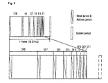
- one frame is divided into several subfields differing in luminous times to implement gray levels of image. And, each of the subfields is divided again into a reset period for generating electric discharge evenly, an address period for selecting a discharge cell, and a sustain period for implementing gray levels according to a discharging number.
- a frame period (16.67ms) corresponding to 1/60 second is divided into eight subfields SF1 To SF8. And, each of the eight subfields SF1 to SF8 is divided into a reset period, an address period, and a sustain period.
- image gray levels can be implemented.
- the subfields of each frame are selected to implement the gray levels in the manner of Table 1.
- Table 1 SF1 SF2 SF3 SF4 SF5 SF6 SF7 SF8 Y1 Y2 Y3 Y8 Y16 Y32 Y64 Y128 0 ⁇ ⁇ ⁇ ⁇ ⁇ ⁇ ⁇ 1 ⁇ ⁇ ⁇ ⁇ ⁇ ⁇ ⁇ 2 ⁇ ⁇ ⁇ ⁇ ⁇ ⁇ 15 ⁇ ⁇ ⁇ ⁇ ⁇ ⁇ 16 ⁇ ⁇ ⁇ ⁇ ⁇ ⁇ 17 ⁇ ⁇ ⁇ ⁇ ⁇ ⁇ ⁇ ⁇ ...
- 'SFx' means an x th subfield
- 'Yz' indicates a brightness weight set to a decimal number for the corresponding subfield ' ⁇ ' indicates a turned-on state of the corresponding subfield
- 'X' indicates a turned-off state of the corresponding subfield
- the subfields bring about sustain discharges to correspond to the brightness weights allocated to them, respectively, thereby representing gray levels corresponding to the brightness weights, respectively.
- the related art PDP brings about a problem that Contour Noise takes place by the discord between a light integration direction and a visual characteristic recognizable by human eyes between the gray levels 15-16, 31-32, 63-64, or 127-128 where a subfield pattern considerably varies.
- a luminosity difference between the two frames becomes a value of '1'.
- the gray value of '127' is displayed as shown in Table 1
- the first to seventh subfields SF1 to SF7 become luminous.
- the gray value of '128' is displayed as shown in Table 1
- the eighth subfield SF8 becomes luminous. Namely, when the subfield pattern is changed from '128' to '127', a subfield pattern timing difference between the two frames becomes big and in case of great movement of a luminous point, Contour Noise occurs.
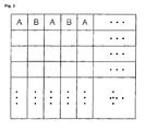
- gray levels A such as e.g., 31 and B such as e.g., 33' are displayed in two neighboring discharge cells, as shown in FIG. 3 , to represent gray level C such as e.g., 32 on the average.
- gray levels A and B such as above are displayed in discharge cells adjacent to each other, as shown in FIG. 3 , to minimize Contour Noise.
- a discharge timing of gray level A is largely different from that of gray level B.
- one discharge occurs in the first to fifth subfields SF1 To SF5 to display gray level A 31.
- the discharges simultaneously occur in the first subfield SF1 only but fail to occur simultaneously in the remaining subfields.
- a high-density Xe panel enables to display an image of high brightness by raising the Xe component of the discharge gas.
- the drive voltage of the high-density Xe panel is set higher than that of the low-density Xe panel, it becomes more probable that the mis-discharge or discharge failure of the high-density Xe panel may occur at lower or higher temperatures when displaying a gray level having a greatly changing subfield pattern on the average.
- US2001/0006379 describes a display apparatus capable of adjusting sub-field number according to brightness wherein the display apparatus may include a temperature detector which provides a signal to an image characteristic determining device.
- US2003/0173903 describes a plasma display apparatus in which the display load ratio of each sub-field is detected and the sustain pulse cycle is changed in response to it.
- a temperature detecting unit is additionally provided to control the number of sustain pulses.
- US6,337,673 describes general features of a plasma display device and a driving device for the display.
- the present invention provides a method and apparatus for driving a plasma display panel as set out in claims 1 and 6 respectively.
- An object of the present invention is to provide a method of driving a plasma display panel and apparatus thereof, by which mis-discharge or mal-discharge can be prevented.
- the method of driving the plasma display panel and apparatus thereof according to the present invention enable to display an image of which contour noise is minimized in a manner of displaying a gray level, of which subfield pattern is greatly changed, on the average in driving a plasma display panel at a normal drive temperature. And, when the plasma display panel is being driven at higher or lower temperatures, the method and apparatus according to the present invention enable to prevent flickering mal-discharge and mis-discharge occurring at higher or lower temperatures in a manner of displaying gray levels as they are.
- An embodiment of the present invention provides a method of driving a plasma display panel as set out in claim 1.
- the second subfield pattern mapping may be carried out in a manner of displaying the gray level subfield pattern greatly changing, on the average in adjacent discharge cells.
- the first subfield pattern mapping may be carried out in a manner of displaying as they are gray levels of valve 2 n with a subfield pattern greatly changing when compared to subfield patterns of nearby gray levels.
- the lower temperatures may range between about 15°C and minus 50 °C and the higher temperatures may range between about 50°C and 100 °C.
- a discharge gas including a Xe gas amounting to at least 5% thereof may be provided within an inner space of the panel.
- An embodiment of the present invention provides an apparatus for driving a plasma display panel as set out in claim 6.
- FIG. 4 is a diagram of a method of driving a plasma display panel according to an embodiment of the present invention.
- a subfield mapping method at lower and higher temperatures is set out to be different from a subfield pattern mapping method at a temperature, hereinafter called normal drive temperature, between the lower and higher temperature thresholds.
- a temperature sensor is attached to the PDP to monitor the drive temperature of the PDP.
- the PDP is driven at the normal drive temperature (16 ⁇ 49.9 °C) in the same manner as in the related art.
- gray levels such as, e.g., 16, 32, 64, and 128 having a greatly changing subfield pattern
- gray levels A such as (e.g., 31 and B such as e.g., 33 in two adjacent discharge cells, as shown in FIG. 3
- gray level C such as e.g., 32 is displayed on the average.
- gray levels having a greatly changing subfield pattern are not displayed on the average when the PDP is driven at the lower or higher temperatures but as they are.
- a gray level having a greatly changing subfield pattern is displayed as it is at the lower or higher temperatures, it is able to solve the problem such as flickering mal-discharge, mis-discharge, and the like.
- gray levels of C such as e.g., 32 or 64 with a subfield pattern greatly changing are directly displayed in the corresponding discharge cell, as shown in FIG. 5 .
- the adjacent discharge cells display identical gray levels, the discharges occur at the same time.
- a specific discharge cell can be supplied with the priming charged particles supplied from the adjacent discharge cells.
- the discharges are facilitated to occur in the discharge cells displaying the same gray level, whereby it is able to prevent a flickering mal-discharge and/or mis-discharge from occurring at the lower or higher temperatures.
- the present invention to a high-density Xe PDP having a component of Xe amounting to at least 5% of discharge gas sealed within the PDP, it is able to prevent a flickering mal-discharge and/or mis-discharge from occurring when the high-density Xe PDP is driven at lower or higher temperatures. Namely, in case of applying the present invention to the high-density Xe PDP, it is able to display an image having high brightness without flickering mal-discharge and/or mis-discharge.
- FIG. 6 is a block diagram of an apparatus for driving a plasma display panel according to an embodiment of the present invention.
- an apparatus for driving a plasma display panel includes a gain adjustment unit 32 connected between a first inverse gamma correction unit 31A and a data alignment unit 35, an error diffusion unit 33, a subfield mapping unit 34, an APL computation unit 36 connected between a second inverse gamma correction unit 31B and a waveform generating unit 37, and a temperature sensor 40 connected to the subfield mapping unit 34.
- Each of the first and second inverse gamma correction units 31A and 31B performs inverse gamma correction on digital video data RGB from an input line 29 to linearly convert brightness for a gray level value of a video signal.
- the gain adjustment unit 32 adjusts an effective gain per data of red, green, and blue to compensate a color temperature.
- the error diffusion unit 33 diffuses a quantization error of the digital video data RGB inputted from the gain adjustment unit 32 into adjacent cells.
- the subfield mapping unit 34 maps the data inputted from the error diffusion unit 33 to a subfield pattern previously stored per bit and then supplies the mapping data to the data alignment unit 35. A detailed operation of the subfield mapping unit 34 will be explained later.
- the data alignment unit 35 supplies the digital video data inputted from the subfield mapping unit 34 to a data driving circuit of a panel 38.
- the data driving circuit which is connected to data electrodes of the panel 38, latches the data inputted from the data alignment unit 35 for one horizontal line and then supplies the latched data to the data electrodes of the panel 38 during onehorizontal period unit.
- the APL computation unit 36 computes an average brightness for each picture frame, i.e., APL (average picture level), for the digital video data RGB inputted from the second inverse correction unit 31B and then outputs sustain pulse number information corresponding to the computed APL.
- APL average picture level
- the waveform generating unit 37 responds to the sustain pulse number information from the APL computation unit to generate a timing control signal and then supplies the timing control signal to a scan drive circuit and sustain drive circuit (not shown in the drawing).
- the scan and sustain drive circuits respond to the timing control signal inputted from the waveform generating unit 37 to supply a sustain pulses to scan electrodes and sustain electrodes of the panel 38 during a sustain period, respectively.
- the temperature sensor 40 detects a drive temperature (peripheral environment temperature) of the panel 38 and then supplies a control signal corresponding to the detected drive temperature to the subfield mapping unit 34.
- the temperature sensor 40 detects the drive temperature (low, high, or normal drive temperature) of the panel 38 and then supplies the control signal corresponding to the detected drive temperature to the subfield mapping unit 34.
- the subfield mapping unit 34 carries out mapping on the sub-field pattern so that a gray level such as, e.g. 16, 32, 64, 128, with a subfield pattern greatly changing , is displayed on average over two adjacent discharge cells. thereby enabling to display an image with minimized contour noise.
- the subfield mapping unit 34 carries out mapping on the subfield patterns so that all levels are directly displayed as they are. Problems such as flickering mal-discharge, mis-discharge, and the like are thereby solved.
Landscapes
- Engineering & Computer Science (AREA)
- Physics & Mathematics (AREA)
- Computer Hardware Design (AREA)
- General Physics & Mathematics (AREA)
- Theoretical Computer Science (AREA)
- Plasma & Fusion (AREA)
- Power Engineering (AREA)
- Control Of Indicators Other Than Cathode Ray Tubes (AREA)
- Control Of Gas Discharge Display Tubes (AREA)
- Gas-Filled Discharge Tubes (AREA)
- Transforming Electric Information Into Light Information (AREA)
Claims (10)
- Verfahren zur Ansteuerung eines Plasma-Anzeigefeldes zur Anzeige von digitalen Videodaten, wobei das Anzeigefeld aufweist:ein vorderes Substrat (10) und ein hinteres Substrat (18), die einander gegenüber liegen,Paare von transparenten Elektroden (12Y, 12Z) auf der Oberfläche des vorderen Substrats (10), das dem hinteren Substrat gegenüber liegt,eine Metallelektrode (13Y, 13Z), die auf jeder der transparenten Elektroden (12Y, 12Z) vorgesehen ist,eine vordere dielektrische Schicht (14), welche die transparenten Elektroden und die Metallelektroden überdeckt,eine Schutzschicht (16), die auf der vorderen dielektrischen Schicht (14) aufbeschichtet ist,Adresselektroden (20X), die auf der Oberfläche des hinteren Substrats (18) ausgebildet sind, das dem vorderen Substrat gegenüber liegt, wobei ihre Richtung die Richtung der transparenten Elektroden kreuzt,eine hintere dielektrische Schicht (22), welche die Adresselektroden (20X) überdeckt,Barriererippen (24), die auf der hinteren dielektrischen Schicht (22) ausgebildet sind,wobei das vordere Substrat und das hintere Substrat und die Barriererippen Entladungszellen bilden,
undeine Fluoreszenzschicht (26), die auf den Teilen der Barriererippen und der hinteren dielektrischen Schicht aufbeschichtet ist, welche die Entladungszellen bilden,wobei das Verfahren folgende Schritte umfasst:Erfassen der Ansteuerungstemperatur des Anzeigefeldes, Mapping der digitalen Videodaten unter Anwendung eines Mappings eines ersten Unterfeld-Musters, wenn die Ansteuerungstemperatur des Anzeigefeldes unterhalb eines ersten Temperatur-Schwellenwertes liegt und wenn die Ansteuerungstemperatur des Anzeigefeldes oberhalb eines zweiten Temperatur-Schwellenwertes liegt, wobei der zweite Temperatur-Schwellenwert höher ist als der erste Temperatur-Schwellenwert,
undMapping der digitalen Videodaten unter Anwendung eines Mappings eines zweiten Unterfeld-Musters, das vom Mapping des ersten Unterfeld-Musters verschieden ist, wenn das Anzeigefeld bei einer Temperatur zwischen dem ersten Temperatur-Schwellenwert und dem zweiten Temperatur-Schwellenwert angesteuert wird. - Verfahren nach Anspruch 1, bei dem, wenn in einer der Entladungszellen ein erster Grauwert eines sich im Vergleich mit den Unterfeld-Mustern in der Nähe liegender Grauwerte stark ändernden Unterfeld-Musters angezeigt werden soll, das Mapping des zweiten Unterfeld-Musters so durchgeführt wird, dass Grauwerte in der Nähe des ersten Grauwertes in der einen Entladungszelle benachbarten Entladungszellen so angezeigt werden, dass im Mittel über die eine Entladungszelle und die benachbarten Entladungszellen der erste Grauwert angezeigt wird.
- Verfahren nach Anspruch 1, bei dem beim Mapping des ersten Unterfeld-Musters jede der Entladungszellen so eingestellt wird, dass ein Grauwert entsprechend der Helligkeits-Gewichtung der einen Entladungszelle in den digitalen Videodaten angezeigt wird.
- Verfahren nach einem der vorhergehenden Ansprüche, bei dem das Muster des Mappings des ersten Unterfeldes zwischen einem ersten Temperatur-Schwellenwert von 15 °C und einer Temperatur von -50 °C und zwischen einem zweiten Temperatur-Schwellenwert von 50 °C und einer Temperatur von 100 °C verwendet wird.
- Verfahren nach einem der vorhergehenden Ansprüche, bei dem ein Entladungsgas, das Xe-Gas in einem Mengenanteil von mindestens 5 % enthält, in einem inneren Raum des Anzeigefeldes vorgesehen wird.
- Vorrichtung zur Ansteuerung eines Plasma-Anzeigefeldes zur Anzeige von digitalen Videodaten, wobei das Anzeigefeld aufweist:ein vorderes Substrat (10) und ein hinteres Substrat (18), die einander gegenüber liegen,Paare von transparenten Elektroden (12Y, 12Z) auf der Oberfläche des vorderen Substrats (10), das dem hinteren Substrat gegenüber liegt,eine Metallelektrode (13Y, 13Z), die auf jeder der transparenten Elektroden (12Y, 12Z) vorgesehen ist,eine vordere dielektrische Schicht (14), welche die transparenten Elektroden und die Metallelektroden überdeckt,eine Schutzschicht (16), die auf der vorderen dielektrischen Schicht (14) aufbeschichtet ist,Adresselektroden (20X), die auf der Oberfläche des hinteren Substrats (18) ausgebildet sind, das dem vorderen Substrat gegenüber liegt, wobei ihre Richtung die Richtung der transparenten Elektroden kreuzt,eine hintere dielektrische Schicht (22), welche die Adresselektroden (20X) überdeckt,Barriererippen (24), die auf der hinteren dielektrischen Schicht (22) ausgebildet sind,wobei das vordere Substrat und das hintere Substrat und die Barriererippen Entladungszellen bilden,
undeine Fluoreszenzschicht (26), die auf den Teilen der Barriererippen und der hinteren dielektrischen Schicht aufbeschichtet ist, welche die Entladungszellen bilden,wobei die Vorrichtung einen Temperatursensor (40), der die Ansteuerungstemperatur des Anzeigefeldes erfasst, und eine Unterfeld-Mappingeinheit (34) aufweist,dadurch gekennzeichnet, dass
die Unterfeld-Mappingeinheit (34) ein Mapping-Schema für Unterfeld-Muster aufweist, das umfasst:Mapping eines ersten Unterfeld-Musters, wenn die Ansteuerungstemperatur des Anzeigefeldes unterhalb eines ersten Temperatur-Schwellenwertes liegt und wenn die Ansteuerungstemperatur des Anzeigefeldes oberhalb eines zweiten Temperatur-Schwellenwertes liegt, wobei der zweite Temperatur-Schwellenwert höher ist als der erste Temperatur-Schwellenwert,
undMapping eines zweiten Unterfeld-Musters, wenn die Ansteuerungstemperatur des Anzeigefeldes zwischen dem ersten Temperatur-Schwellenwert und dem zweiten Temperatur-Schwellenwert liegt. - Vorrichtung nach Anspruch 6, bei der das Mapping des zweiten Unterfeld-Musters so ausgelegt ist, dass, wenn in einer der Entladungszellen ein erster Grauwert eines sich im Vergleich mit den Unterfeld-Mustern in der Nähe liegender Grauwerte stark ändernden Unterfeld-Musters angezeigt werden soll, die Unterfeld-Mappingeinheit dafür geeignet ist, dass das Mapping des zweiten Unterfeld-Musters so durchgeführt wird, dass Grauwerte in der Nähe des ersten Grauwertes in der einen Entladungszelle und in benachbarten Entladungszellen so angezeigt werden, dass im Mittel über die eine Entladungszelle und die benachbarten Entladungszellen der erste Grauwert angezeigt wird.
- Vorrichtung nach Anspruch 6, bei der die Unterfeld-Mappingeinheit (34) so ausgelegt ist, dass das Mapping des ersten Unterfeld-Musters so eingestellt wird, dass jede der Entladungszellen einen Grauwert entsprechend der Helligkeits-Gewichtung der einen Entladungszelle in den digitalen Videodaten anzeigt.
- Vorrichtung nach einem der Ansprüche 6 bis 8, bei der das Muster des Mappings des ersten Unterfeldes zwischen einem ersten Temperatur-Schwellenwert von 15 °C und einer Temperatur von -50 °C und zwischen einem zweiten Temperatur-Schwellenwert von 50 °C und einer Temperatur von 100 °C verwendet wird.
- Vorrichtung nach einem der Ansprüche 6 bis 9, bei der ein Entladungsgas, das Xe-Gas in einem Mengenanteil von mindestens 5 % enthält, in einem inneren Raum des Anzeigefeldes vorgesehen ist.
Applications Claiming Priority (2)
| Application Number | Priority Date | Filing Date | Title |
|---|---|---|---|
| KR10-2003-0071500A KR100509765B1 (ko) | 2003-10-14 | 2003-10-14 | 플라즈마 디스플레이 패널의 구동방법 및 구동장치 |
| KR2003071500 | 2003-10-14 |
Publications (3)
| Publication Number | Publication Date |
|---|---|
| EP1524645A2 EP1524645A2 (de) | 2005-04-20 |
| EP1524645A3 EP1524645A3 (de) | 2006-05-31 |
| EP1524645B1 true EP1524645B1 (de) | 2010-12-08 |
Family
ID=34374270
Family Applications (1)
| Application Number | Title | Priority Date | Filing Date |
|---|---|---|---|
| EP04256288A Expired - Lifetime EP1524645B1 (de) | 2003-10-14 | 2004-10-12 | Verfahren und Vorrichtung zur Ansteuerung eines Plasma-Anzeigefeldes |
Country Status (8)
| Country | Link |
|---|---|
| US (1) | US7425935B2 (de) |
| EP (1) | EP1524645B1 (de) |
| JP (1) | JP2005122184A (de) |
| KR (1) | KR100509765B1 (de) |
| CN (1) | CN100401351C (de) |
| AT (1) | ATE491200T1 (de) |
| DE (1) | DE602004030404D1 (de) |
| TW (1) | TWI269249B (de) |
Families Citing this family (3)
| Publication number | Priority date | Publication date | Assignee | Title |
|---|---|---|---|---|
| KR100738815B1 (ko) * | 2005-08-23 | 2007-07-12 | 엘지전자 주식회사 | 플라즈마 디스플레이 패널의 구동장치 및 방법 |
| EP1990795A4 (de) * | 2006-02-28 | 2009-12-16 | Panasonic Corp | Ansteuerverfahren für eine plasmaanzeigetafel und plasmaanzeigevorrichtung |
| KR100778418B1 (ko) * | 2006-12-12 | 2007-11-22 | 삼성에스디아이 주식회사 | 플라즈마 표시 장치 및 그 구동 방법 |
Family Cites Families (14)
| Publication number | Priority date | Publication date | Assignee | Title |
|---|---|---|---|---|
| JP2900966B2 (ja) * | 1993-04-02 | 1999-06-02 | 株式会社富士通ゼネラル | 画像表示方法およびその装置 |
| JPH07114360A (ja) * | 1993-10-15 | 1995-05-02 | Fujitsu General Ltd | 表示映像の処理方法およびその装置 |
| JP2994630B2 (ja) * | 1997-12-10 | 1999-12-27 | 松下電器産業株式会社 | 明るさによるサブフィールド数調整可能な表示装置 |
| JP2994634B2 (ja) * | 1997-12-10 | 1999-12-27 | 松下電器産業株式会社 | 表示装置 |
| JP2000047634A (ja) * | 1998-07-29 | 2000-02-18 | Pioneer Electron Corp | プラズマディスプレイ装置の駆動方法 |
| JP2000181395A (ja) * | 1998-12-11 | 2000-06-30 | Sharp Corp | マトリックス型表示装置 |
| JP2000227780A (ja) * | 1999-02-08 | 2000-08-15 | Mitsubishi Electric Corp | 気体放電型表示装置およびその駆動方法 |
| JP4360450B2 (ja) * | 1999-06-09 | 2009-11-11 | 株式会社日立プラズマパテントライセンシング | 表示装置 |
| JP3270435B2 (ja) * | 1999-10-04 | 2002-04-02 | 松下電器産業株式会社 | 表示装置およびその輝度制御方法 |
| JP4660036B2 (ja) * | 2000-09-01 | 2011-03-30 | パナソニック株式会社 | プラズマディスプレイ装置およびその駆動方法 |
| JP4795577B2 (ja) * | 2001-08-17 | 2011-10-19 | エルジー エレクトロニクス インコーポレイティド | プラズマディスプレイ装置 |
| US7215316B2 (en) * | 2001-10-25 | 2007-05-08 | Lg Electronics Inc. | Apparatus and method for driving plasma display panel |
| EP1331624A1 (de) * | 2002-01-23 | 2003-07-30 | Koninklijke Philips Electronics N.V. | Methode und Vorrichtung zur Ansteuerung eines Plasmabildschirms |
| JP4308488B2 (ja) * | 2002-03-12 | 2009-08-05 | 日立プラズマディスプレイ株式会社 | プラズマディスプレイ装置 |
-
2003
- 2003-10-14 KR KR10-2003-0071500A patent/KR100509765B1/ko not_active Expired - Fee Related
-
2004
- 2004-10-12 DE DE602004030404T patent/DE602004030404D1/de not_active Expired - Lifetime
- 2004-10-12 AT AT04256288T patent/ATE491200T1/de not_active IP Right Cessation
- 2004-10-12 EP EP04256288A patent/EP1524645B1/de not_active Expired - Lifetime
- 2004-10-13 TW TW093131006A patent/TWI269249B/zh not_active IP Right Cessation
- 2004-10-14 CN CNB2004100881227A patent/CN100401351C/zh not_active Expired - Fee Related
- 2004-10-14 US US10/963,601 patent/US7425935B2/en not_active Expired - Fee Related
- 2004-10-14 JP JP2004300700A patent/JP2005122184A/ja active Pending
Also Published As
| Publication number | Publication date |
|---|---|
| JP2005122184A (ja) | 2005-05-12 |
| US20050104810A1 (en) | 2005-05-19 |
| DE602004030404D1 (de) | 2011-01-20 |
| ATE491200T1 (de) | 2010-12-15 |
| TW200515344A (en) | 2005-05-01 |
| US7425935B2 (en) | 2008-09-16 |
| KR100509765B1 (ko) | 2005-08-24 |
| CN1629921A (zh) | 2005-06-22 |
| EP1524645A2 (de) | 2005-04-20 |
| EP1524645A3 (de) | 2006-05-31 |
| TWI269249B (en) | 2006-12-21 |
| CN100401351C (zh) | 2008-07-09 |
| KR20050036045A (ko) | 2005-04-20 |
Similar Documents
| Publication | Publication Date | Title |
|---|---|---|
| KR100352861B1 (ko) | Ac형 pdp의 구동방법 | |
| US7911417B2 (en) | Method and apparatus for expressing gray levels in a plasma display panel | |
| KR100524312B1 (ko) | 플라즈마 디스플레이 패널의 초기화 제어방법 및 장치 | |
| JP2005165328A (ja) | プラズマディスプレイパネルの駆動装置及び方法 | |
| KR20020061500A (ko) | 플라즈마 디스플레이 패널의 소수값 계조 표현방법 및 장치 | |
| EP1526501B1 (de) | Verfahren und Vorrichtung zur Ansteuerung einer Plasmaanzeigetafel | |
| JP2004318163A (ja) | プラズマディスプレイパネルの駆動方法および装置 | |
| EP1524645B1 (de) | Verfahren und Vorrichtung zur Ansteuerung eines Plasma-Anzeigefeldes | |
| EP1526499B1 (de) | Verfahren und Vorrichtung zur Ansteuerung einer Plasmaanzeigetafel | |
| US20070030214A1 (en) | Plasma display apparatus and driving method thereof | |
| KR100493915B1 (ko) | 플라즈마 디스플레이 패널의 구동 방법 및 장치 | |
| US7843405B2 (en) | Plasma display apparatus and method of driving the same | |
| JP2006528791A (ja) | プラズマディスプレイパネルの駆動装置およびその方法 | |
| EP1522987A2 (de) | Verfahren zur Ansteuerung einer Plasmaanzeigetafel | |
| KR100488150B1 (ko) | 플라즈마 디스플레이 패널의 구동장치 및 구동방법 | |
| KR100486910B1 (ko) | 플라즈마 디스플레이 패널 및 그의 구동방법 | |
| KR100738815B1 (ko) | 플라즈마 디스플레이 패널의 구동장치 및 방법 | |
| KR20050056828A (ko) | 플라즈마 디스플레이 패널의 구동방법 및 장치 | |
| KR20050106697A (ko) | 플라즈마 디스플레이 패널의 구동방법 및 장치 | |
| KR20080020341A (ko) | 플라즈마 디스플레이 패널의 구동 방법 | |
| KR20040072891A (ko) | 플라즈마 디스플레이 패널의 구동 방법 및 장치 | |
| KR20040057899A (ko) | 플라즈마 디스플레이 패널의 구동방법 및 장치 | |
| KR20050099222A (ko) | 플라즈마 디스플레이 패널의 구동방법 및 장치 | |
| KR20060127539A (ko) | 플라즈마 디스플레이 장치 및 플라즈마 디스플레이 패널의구동 방법 |
Legal Events
| Date | Code | Title | Description |
|---|---|---|---|
| PUAI | Public reference made under article 153(3) epc to a published international application that has entered the european phase |
Free format text: ORIGINAL CODE: 0009012 |
|
| AK | Designated contracting states |
Kind code of ref document: A2 Designated state(s): AT BE BG CH CY CZ DE DK EE ES FI FR GB GR HU IE IT LI LU MC NL PL PT RO SE SI SK TR |
|
| AX | Request for extension of the european patent |
Extension state: AL HR LT LV MK |
|
| RIN1 | Information on inventor provided before grant (corrected) |
Inventor name: SIM, SOO SEOK Inventor name: KIM,YOUNG DAEPDP DEVELOPMENT SECTION, PDP DEPT. |
|
| PUAL | Search report despatched |
Free format text: ORIGINAL CODE: 0009013 |
|
| AK | Designated contracting states |
Kind code of ref document: A3 Designated state(s): AT BE BG CH CY CZ DE DK EE ES FI FR GB GR HU IE IT LI LU MC NL PL PT RO SE SI SK TR |
|
| AX | Request for extension of the european patent |
Extension state: AL HR LT LV MK |
|
| 17P | Request for examination filed |
Effective date: 20060607 |
|
| 17Q | First examination report despatched |
Effective date: 20060717 |
|
| AKX | Designation fees paid |
Designated state(s): AT BE BG CH CY CZ DE DK EE ES FI FR GB GR HU IE IT LI LU MC NL PL PT RO SE SI SK TR |
|
| GRAJ | Information related to disapproval of communication of intention to grant by the applicant or resumption of examination proceedings by the epo deleted |
Free format text: ORIGINAL CODE: EPIDOSDIGR1 |
|
| GRAP | Despatch of communication of intention to grant a patent |
Free format text: ORIGINAL CODE: EPIDOSNIGR1 |
|
| RAP1 | Party data changed (applicant data changed or rights of an application transferred) |
Owner name: LG ELECTRONICS INC. |
|
| RIN1 | Information on inventor provided before grant (corrected) |
Inventor name: SIM, SOO SEOK Inventor name: KIM,YOUNG DAE |
|
| GRAS | Grant fee paid |
Free format text: ORIGINAL CODE: EPIDOSNIGR3 |
|
| GRAA | (expected) grant |
Free format text: ORIGINAL CODE: 0009210 |
|
| AK | Designated contracting states |
Kind code of ref document: B1 Designated state(s): AT BE BG CH CY CZ DE DK EE ES FI FR GB GR HU IE IT LI LU MC NL PL PT RO SE SI SK TR |
|
| REG | Reference to a national code |
Ref country code: GB Ref legal event code: FG4D |
|
| REG | Reference to a national code |
Ref country code: CH Ref legal event code: EP |
|
| REG | Reference to a national code |
Ref country code: IE Ref legal event code: FG4D |
|
| REG | Reference to a national code |
Ref country code: NL Ref legal event code: T3 |
|
| REF | Corresponds to: |
Ref document number: 602004030404 Country of ref document: DE Date of ref document: 20110120 Kind code of ref document: P |
|
| PG25 | Lapsed in a contracting state [announced via postgrant information from national office to epo] |
Ref country code: AT Free format text: LAPSE BECAUSE OF FAILURE TO SUBMIT A TRANSLATION OF THE DESCRIPTION OR TO PAY THE FEE WITHIN THE PRESCRIBED TIME-LIMIT Effective date: 20101208 Ref country code: FI Free format text: LAPSE BECAUSE OF FAILURE TO SUBMIT A TRANSLATION OF THE DESCRIPTION OR TO PAY THE FEE WITHIN THE PRESCRIBED TIME-LIMIT Effective date: 20101208 Ref country code: SI Free format text: LAPSE BECAUSE OF FAILURE TO SUBMIT A TRANSLATION OF THE DESCRIPTION OR TO PAY THE FEE WITHIN THE PRESCRIBED TIME-LIMIT Effective date: 20101208 Ref country code: SE Free format text: LAPSE BECAUSE OF FAILURE TO SUBMIT A TRANSLATION OF THE DESCRIPTION OR TO PAY THE FEE WITHIN THE PRESCRIBED TIME-LIMIT Effective date: 20101208 Ref country code: CY Free format text: LAPSE BECAUSE OF FAILURE TO SUBMIT A TRANSLATION OF THE DESCRIPTION OR TO PAY THE FEE WITHIN THE PRESCRIBED TIME-LIMIT Effective date: 20101208 Ref country code: BG Free format text: LAPSE BECAUSE OF FAILURE TO SUBMIT A TRANSLATION OF THE DESCRIPTION OR TO PAY THE FEE WITHIN THE PRESCRIBED TIME-LIMIT Effective date: 20110308 |
|
| PG25 | Lapsed in a contracting state [announced via postgrant information from national office to epo] |
Ref country code: GR Free format text: LAPSE BECAUSE OF FAILURE TO SUBMIT A TRANSLATION OF THE DESCRIPTION OR TO PAY THE FEE WITHIN THE PRESCRIBED TIME-LIMIT Effective date: 20110309 Ref country code: CZ Free format text: LAPSE BECAUSE OF FAILURE TO SUBMIT A TRANSLATION OF THE DESCRIPTION OR TO PAY THE FEE WITHIN THE PRESCRIBED TIME-LIMIT Effective date: 20101208 Ref country code: EE Free format text: LAPSE BECAUSE OF FAILURE TO SUBMIT A TRANSLATION OF THE DESCRIPTION OR TO PAY THE FEE WITHIN THE PRESCRIBED TIME-LIMIT Effective date: 20101208 Ref country code: ES Free format text: LAPSE BECAUSE OF FAILURE TO SUBMIT A TRANSLATION OF THE DESCRIPTION OR TO PAY THE FEE WITHIN THE PRESCRIBED TIME-LIMIT Effective date: 20110319 Ref country code: BE Free format text: LAPSE BECAUSE OF FAILURE TO SUBMIT A TRANSLATION OF THE DESCRIPTION OR TO PAY THE FEE WITHIN THE PRESCRIBED TIME-LIMIT Effective date: 20101208 Ref country code: PT Free format text: LAPSE BECAUSE OF FAILURE TO SUBMIT A TRANSLATION OF THE DESCRIPTION OR TO PAY THE FEE WITHIN THE PRESCRIBED TIME-LIMIT Effective date: 20110408 |
|
| PG25 | Lapsed in a contracting state [announced via postgrant information from national office to epo] |
Ref country code: PL Free format text: LAPSE BECAUSE OF FAILURE TO SUBMIT A TRANSLATION OF THE DESCRIPTION OR TO PAY THE FEE WITHIN THE PRESCRIBED TIME-LIMIT Effective date: 20101208 Ref country code: SK Free format text: LAPSE BECAUSE OF FAILURE TO SUBMIT A TRANSLATION OF THE DESCRIPTION OR TO PAY THE FEE WITHIN THE PRESCRIBED TIME-LIMIT Effective date: 20101208 Ref country code: RO Free format text: LAPSE BECAUSE OF FAILURE TO SUBMIT A TRANSLATION OF THE DESCRIPTION OR TO PAY THE FEE WITHIN THE PRESCRIBED TIME-LIMIT Effective date: 20101208 |
|
| PLBE | No opposition filed within time limit |
Free format text: ORIGINAL CODE: 0009261 |
|
| STAA | Information on the status of an ep patent application or granted ep patent |
Free format text: STATUS: NO OPPOSITION FILED WITHIN TIME LIMIT |
|
| PG25 | Lapsed in a contracting state [announced via postgrant information from national office to epo] |
Ref country code: DK Free format text: LAPSE BECAUSE OF FAILURE TO SUBMIT A TRANSLATION OF THE DESCRIPTION OR TO PAY THE FEE WITHIN THE PRESCRIBED TIME-LIMIT Effective date: 20101208 |
|
| 26N | No opposition filed |
Effective date: 20110909 |
|
| PG25 | Lapsed in a contracting state [announced via postgrant information from national office to epo] |
Ref country code: IT Free format text: LAPSE BECAUSE OF FAILURE TO SUBMIT A TRANSLATION OF THE DESCRIPTION OR TO PAY THE FEE WITHIN THE PRESCRIBED TIME-LIMIT Effective date: 20101208 |
|
| REG | Reference to a national code |
Ref country code: DE Ref legal event code: R097 Ref document number: 602004030404 Country of ref document: DE Effective date: 20110909 |
|
| PG25 | Lapsed in a contracting state [announced via postgrant information from national office to epo] |
Ref country code: MC Free format text: LAPSE BECAUSE OF NON-PAYMENT OF DUE FEES Effective date: 20111031 |
|
| REG | Reference to a national code |
Ref country code: CH Ref legal event code: PL |
|
| PG25 | Lapsed in a contracting state [announced via postgrant information from national office to epo] |
Ref country code: LI Free format text: LAPSE BECAUSE OF NON-PAYMENT OF DUE FEES Effective date: 20111031 Ref country code: CH Free format text: LAPSE BECAUSE OF NON-PAYMENT OF DUE FEES Effective date: 20111031 |
|
| REG | Reference to a national code |
Ref country code: IE Ref legal event code: MM4A |
|
| PG25 | Lapsed in a contracting state [announced via postgrant information from national office to epo] |
Ref country code: IE Free format text: LAPSE BECAUSE OF NON-PAYMENT OF DUE FEES Effective date: 20111012 |
|
| PG25 | Lapsed in a contracting state [announced via postgrant information from national office to epo] |
Ref country code: LU Free format text: LAPSE BECAUSE OF NON-PAYMENT OF DUE FEES Effective date: 20111012 |
|
| PG25 | Lapsed in a contracting state [announced via postgrant information from national office to epo] |
Ref country code: TR Free format text: LAPSE BECAUSE OF FAILURE TO SUBMIT A TRANSLATION OF THE DESCRIPTION OR TO PAY THE FEE WITHIN THE PRESCRIBED TIME-LIMIT Effective date: 20101208 |
|
| PG25 | Lapsed in a contracting state [announced via postgrant information from national office to epo] |
Ref country code: HU Free format text: LAPSE BECAUSE OF FAILURE TO SUBMIT A TRANSLATION OF THE DESCRIPTION OR TO PAY THE FEE WITHIN THE PRESCRIBED TIME-LIMIT Effective date: 20101208 |
|
| PGFP | Annual fee paid to national office [announced via postgrant information from national office to epo] |
Ref country code: NL Payment date: 20130911 Year of fee payment: 10 |
|
| PGFP | Annual fee paid to national office [announced via postgrant information from national office to epo] |
Ref country code: FR Payment date: 20130912 Year of fee payment: 10 Ref country code: GB Payment date: 20130911 Year of fee payment: 10 |
|
| PGFP | Annual fee paid to national office [announced via postgrant information from national office to epo] |
Ref country code: DE Payment date: 20130912 Year of fee payment: 10 |
|
| REG | Reference to a national code |
Ref country code: DE Ref legal event code: R119 Ref document number: 602004030404 Country of ref document: DE |
|
| REG | Reference to a national code |
Ref country code: NL Ref legal event code: V1 Effective date: 20150501 |
|
| GBPC | Gb: european patent ceased through non-payment of renewal fee |
Effective date: 20141012 |
|
| PG25 | Lapsed in a contracting state [announced via postgrant information from national office to epo] |
Ref country code: DE Free format text: LAPSE BECAUSE OF NON-PAYMENT OF DUE FEES Effective date: 20150501 Ref country code: GB Free format text: LAPSE BECAUSE OF NON-PAYMENT OF DUE FEES Effective date: 20141012 |
|
| REG | Reference to a national code |
Ref country code: FR Ref legal event code: ST Effective date: 20150630 |
|
| PG25 | Lapsed in a contracting state [announced via postgrant information from national office to epo] |
Ref country code: FR Free format text: LAPSE BECAUSE OF NON-PAYMENT OF DUE FEES Effective date: 20141031 Ref country code: NL Free format text: LAPSE BECAUSE OF NON-PAYMENT OF DUE FEES Effective date: 20150501 |