EP1523114B1 - Optisches Übertragungssystem - Google Patents
Optisches Übertragungssystem Download PDFInfo
- Publication number
- EP1523114B1 EP1523114B1 EP04023795A EP04023795A EP1523114B1 EP 1523114 B1 EP1523114 B1 EP 1523114B1 EP 04023795 A EP04023795 A EP 04023795A EP 04023795 A EP04023795 A EP 04023795A EP 1523114 B1 EP1523114 B1 EP 1523114B1
- Authority
- EP
- European Patent Office
- Prior art keywords
- signal
- optical transmission
- transmission path
- optical
- test signal
- Prior art date
- Legal status (The legal status is an assumption and is not a legal conclusion. Google has not performed a legal analysis and makes no representation as to the accuracy of the status listed.)
- Expired - Lifetime
Links
- 230000003287 optical effect Effects 0.000 title claims abstract description 176
- 230000005540 biological transmission Effects 0.000 title claims abstract description 163
- 238000012360 testing method Methods 0.000 claims abstract description 96
- 230000006854 communication Effects 0.000 claims abstract description 25
- 238000004891 communication Methods 0.000 claims abstract description 25
- 238000001514 detection method Methods 0.000 claims abstract description 13
- 238000003672 processing method Methods 0.000 claims description 8
- 238000000034 method Methods 0.000 claims description 4
- 238000012545 processing Methods 0.000 description 45
- 239000013307 optical fiber Substances 0.000 description 13
- 230000000977 initiatory effect Effects 0.000 description 9
- 238000010586 diagram Methods 0.000 description 6
- 230000004044 response Effects 0.000 description 6
- 230000009467 reduction Effects 0.000 description 5
- 230000007704 transition Effects 0.000 description 5
- 230000006870 function Effects 0.000 description 4
- 238000012544 monitoring process Methods 0.000 description 4
- 238000011084 recovery Methods 0.000 description 3
- 230000000007 visual effect Effects 0.000 description 3
- GNFTZDOKVXKIBK-UHFFFAOYSA-N 3-(2-methoxyethoxy)benzohydrazide Chemical compound COCCOC1=CC=CC(C(=O)NN)=C1 GNFTZDOKVXKIBK-UHFFFAOYSA-N 0.000 description 2
- FGUUSXIOTUKUDN-IBGZPJMESA-N C1(=CC=CC=C1)N1C2=C(NC([C@H](C1)NC=1OC(=NN=1)C1=CC=CC=C1)=O)C=CC=C2 Chemical compound C1(=CC=CC=C1)N1C2=C(NC([C@H](C1)NC=1OC(=NN=1)C1=CC=CC=C1)=O)C=CC=C2 FGUUSXIOTUKUDN-IBGZPJMESA-N 0.000 description 2
- 230000007257 malfunction Effects 0.000 description 2
- 230000003213 activating effect Effects 0.000 description 1
- 230000007175 bidirectional communication Effects 0.000 description 1
- 238000012790 confirmation Methods 0.000 description 1
- 238000005516 engineering process Methods 0.000 description 1
- 239000000284 extract Substances 0.000 description 1
- 230000002093 peripheral effect Effects 0.000 description 1
- 230000003252 repetitive effect Effects 0.000 description 1
- 230000000630 rising effect Effects 0.000 description 1
- 239000004065 semiconductor Substances 0.000 description 1
- 238000007493 shaping process Methods 0.000 description 1
- 230000011664 signaling Effects 0.000 description 1
- 230000005236 sound signal Effects 0.000 description 1
- 230000001052 transient effect Effects 0.000 description 1
Images


Classifications
-
- H—ELECTRICITY
- H04—ELECTRIC COMMUNICATION TECHNIQUE
- H04B—TRANSMISSION
- H04B10/00—Transmission systems employing electromagnetic waves other than radio-waves, e.g. infrared, visible or ultraviolet light, or employing corpuscular radiation, e.g. quantum communication
- H04B10/03—Arrangements for fault recovery
-
- H—ELECTRICITY
- H04—ELECTRIC COMMUNICATION TECHNIQUE
- H04B—TRANSMISSION
- H04B10/00—Transmission systems employing electromagnetic waves other than radio-waves, e.g. infrared, visible or ultraviolet light, or employing corpuscular radiation, e.g. quantum communication
- H04B10/07—Arrangements for monitoring or testing transmission systems; Arrangements for fault measurement of transmission systems
- H04B10/075—Arrangements for monitoring or testing transmission systems; Arrangements for fault measurement of transmission systems using an in-service signal
- H04B10/077—Arrangements for monitoring or testing transmission systems; Arrangements for fault measurement of transmission systems using an in-service signal using a supervisory or additional signal
- H04B10/0775—Performance monitoring and measurement of transmission parameters
-
- H—ELECTRICITY
- H04—ELECTRIC COMMUNICATION TECHNIQUE
- H04B—TRANSMISSION
- H04B2210/00—Indexing scheme relating to optical transmission systems
- H04B2210/08—Shut-down or eye-safety
Definitions
- the present invention relates to an optical transmission system which transmits and receives an optical signal through an optical transmission path, for example, an optical fiber cable or the like.
- JP-A-2000131566 discloses a front plate structure for an optical connector which comprises an optical shutter in an optical output part of an optical transceiver, and uses the optical shutter to block an optical beam if an optical connector or an optical fiber cable comes off the transceiver.
- JP-A-2003032189 discloses an optical transceiver which measures the level of a received optical signal from a destination device connected through an optical fiber cable, determines that a trouble has occurred such as a broken optical fiber cable, a detached optical connector, or the like when the level falls below a predetermined threshold, and reduces the power of its optical output part.
- an optical shutter which involves a mechanical structure causes a more complicated structure of the apparatus, and an increase in susceptibility due to mechanical operations is not negligible.
- a method of detecting the level of received light additionally requires elements and circuits for detecting the level of received light, causing a complicated structure of the apparatus, like the former solution.
- the level of received light largely varies due to an attenuation factor of an optical fiber cable used as a transmission path, and a dynamic range of a transmitted optical signal, a threshold improperly set for determining the level of received light would cause frequent malfunctions. Further, it would be desirable to provide a fault detecting system which is stable in detecting operation and does not malfunction even with a transient signal error due to the introduction of noise or the like.
- US 6,433,905 discloses equipment of a hybrid fiber-coaxial network having a frequency agile transponder connected thereto.
- Each frequency agile transponder includes a transmitter and a receiver which are connectable to a coaxial line of the network. Bidirectional communication can occur between a controller and each frequency agile transponder via the network.
- the frequency agile transponder has analog inputs/outputs connectable to test points.
- a computer can store the test result data for subsequent retrieval and/or generate an alarm when a particular test result data exceeds a predetermined limit.
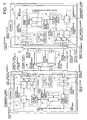
- Fig. 1 shows an exemplary configuration of an optical transmission system and a optical transceiver 10 according to a first embodiment of the present invention.
- a terminal A is a supply controller for a so-called audio visual source such as a video disk reproducing apparatus, a digital broadcast receiver, and the like.
- a terminal B in turn is an audio visual information display terminal device, for example, a wall-mounted television, a large screen display panel, or the like.
- the optical transceiver 10 is built in each of the two terminals, and the optical transceivers 10 contained in the respective terminals are connected to each other through optical connectors 20 and an optical fiber cable 30.
- the optical transceiver 10 mainly comprises a signal generator part 11, an optical transmitter unit 12, a light receiver unit 13, a signal state determination unit 14, and a control unit 15.
- the signal generator part 11 mainly comprises a transmission signal generator circuit, and an output power setting circuit.
- the transmission signal generator circuit adds a synchronization signal and an error correcting code to a data signal representative of video, audio, and the like, transmitted from the terminal A to the terminal B, to generate an electric transmission signal in a predetermined transmission format.
- the transmission signal generator circuit also switches the number of times a transmission format for transmission data is repeated, and a format for the transmission data to a test mode, later described, in accordance with a state determination signal from the signal state determination part 14, later described.
- the output power setting circuit in turn, generates an output control signal for adjusting the output power of an optical transmission signal output from the optical transmitter part 12 in accordance with the state determination signal.
- the optical transmitter part 12 is composed of a light emitting element such as a semiconductor laser diode, a monitor light receiving element such as a photodiode, a light emitting element driving circuit, and an optical output control circuit.
- the light emitting element is applied with a modulated current signal from the light emitting element driving circuit in combination with a bias current signal from the optical output control circuit.
- the light emitting element driving circuit generates a modulated current signal in accordance with the electric transmission signal, and the modulated current signal is applied to the light emitting element.
- the light emitting element is excited by the modulated current signal applied thereto, and outputs an optical transmission signal having output power in accordance with the level of the modulated current signal, i.e., high or low level, to the optical fiber cable 30 through the optical connector 20.
- the output of the optical transmission signal is monitored by the monitor light receiving element which generates an electric monitor signal in accordance with the output power of the optical transmission signal, and supplies the electric monitor signal to the optical output control circuit.
- the optical output control circuit adjusts the value of the bias current signal such that the value of the electric monitor signal is constant.
- the optical output control circuit is also supplied with an output control signal from the signal generator part 11, so that the optical output control circuit adjusts the value of the bias current signal in accordance with the output control signal to increase or decrease the output power of the optical transmission signal.
- the light receiver part 13 mainly comprises a light receiving element such as a photodiode, and an identification circuit.
- a light receiving element such as a photodiode
- an identification circuit As an optical reception signal is input to the light receiving element from the optical transceiver 10 in the terminal B through the optical fiber cable 30 and optical connector 20, the light receiving element generates a light reception current signal of a magnitude conforming to the high or low level of the optical reception signal, and supplies the light reception current signal to the identification circuit.
- the identification circuit amplifies the light reception current signal, and performs signal processing such as waveform shaping on this signal to generate an electric reception signal.
- the signal state determination part 14 mainly comprises a signal state detector circuit, a reference value generator circuit, and a comparison/determination circuit.
- the signal state detector circuit extracts a synchronization signal, an error correcting code, and the like from the electric reception signal to determine whether a receiving condition is good or bad.
- the comparison/determination circuit compares the result of the determination as to good or bad of the receiving condition with a reference value, indicative of goodness/badness of the receiving condition, generated by the reference value generator circuit to generate a predetermined condition determination signal which is supplied to the signal generator circuit 11.
- the control part 15 mainly comprises a microprocessor, a memory circuit such as RAM, ROM, and the like, and an associated peripheral circuit.
- the control part 15 totally controls the entire optical transceiver 10, and is connected to the components described above through a bus line, not shown, and a variety of control and monitoring lines.
- the ROM in the memory circuit of the control part 15 stores a variety of programs for defining the operation of the optical transceiver 10.
- the microprocessor executes such programs step by step in synchronism with the clock signal to execute a variety of processing in the optical transceiver 10.
- the RAM in the memory circuit in turn is used as an temporary storage area for a variety of flags, processed values, or a variety of count values, and the like in course of the operational processing.
- Arrows in Fig. 1 indicate flows of main signals between the respective components described above.
- a response signal, a monitoring signal, and the like for the main signals may be transmitted in the directions opposite to those indicated by the arrows.
- the arrows in the figures indicate conceptual flows of signals between respective components, and in the actual optical transceiver, signals need not be transmitted and received along paths as indicated by the arrows.
- a variety of control signals and state monitoring signals may be once collected in the control part 15 and then transmitted to associated components through the control part 15.
- Fig. 1 represents each of the signal generator part 11, signal state determination part 14, and the like as an independent component, part or all of functions provided by these components may be implemented by software processing with a program stored in the memory of the control part 15. Alternatively, those components which exist independently of one another may be used in combination with part of functions of respective components implemented by software processing.
- each of the terminals A, B comprises a variety of circuits for performing essential functions of each terminal, for example, a video disk reproducing apparatus, a wall-mounted television, and the like, other than the optical transceiver 10, these circuits are not directly related to the implementation of the present invention, so that description thereon is omitted.
- step a in Fig. 2 assume that some fault occurs on a transmission path: terminal A --> terminal B, for example, detachment of the optical connector 20, breakage of the optical fiber cable 30, or the like.
- This fault causes the terminal B to experience a failure in correctly detecting the synchronization signal included in received data, or a reduction in error rate of received data.
- the signal state determination part 14 of the terminal B evaluates such a state in the form of an error rate, an error correcting ratio, or the like with respect to a received signal, compares the value with a reference value indicative of a normal communication state, and determines that a trouble occurs in a signal receiving condition when the value exceeds the predetermined reference value (step b).
- the signal generator part 11 switches the format of transmission data to test data, and generates an output control signal for reducing the power of an optical transmission signal which is output to the optical transmitter part 12 (step c).
- a variety of formats can be contemplated for the test data depending on conditions including a signaling scheme used in the optical transmission system, an operating policy of the system, and the like.
- a data portion may be set in a bit pattern which cannot be generally taken by data, as shown in Fig. 3B, for use as test data.
- an interval between synchronization signals included in the transmission format may be defined as a signal untransmitted portion, and this transmission format may be used to identify the test data.
- a modulation method or a signal speed of a transmission signal may be made different from normal data, so that test data is recognized.
- predetermined test data is transmitted from the optical transmitter part 12 of the terminal B onto the transmission path: terminal B --> terminal A, as an optical transmission signal having a reduced output power.
- an optical transmission signal from the terminal B is communicated to the terminal A through a transmission path: terminal B --> terminal A, and when the signal state determination part 14 of the terminal A determines that the received data is test data, the signal state determination part 14 of the terminal A notifies the signal generator part 11 of this information through a state determination signal (step e).
- the signal generator part 11 switches the format of the transmission data to the aforementioned test data, and supplies the optical transmitter part 12 with an output control signal for reducing the output power of the optical transmission signal (step f).
- the optical transmitter part 12 may be supplied with an output control signal for forcedly stopping the output of the optical transmission signal.
- Such a transmission stopping operation based on so-called timeout may be implemented in the optical transceiver 10 by any of the terminal A and terminal B, or may be implemented by the optical transceiver 10 in both the terminal A and terminal B.
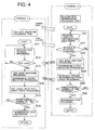
- the flow chart of Fig. 4 represents processing programs for the operation of the optical transceiver 10 incorporated in each of the terminals A, B which is related to the sequence processing in Fig. 2.
- a program related to the processing in the terminal A is called the "test data reception processing task”
- a program related to the processing in the terminal B is called the “received data determination processing task.”
- This task may be repeatedly initiated at all times during the operation of the terminal B, or may be initiated in synchronism with reception of data from the terminal A.
- the microprocessor in the control part 15 determines a receiving condition based on a state determination signal from the signal state determination part 14 at step S21. As a result of the determination, if no trouble is recognized in the receiving condition, the CPU returns to step S21 to repeat the foregoing processing (step S22). To avoid preventing the execution of other processing executed by the CPU due to the continuing repetitive processing, the control of the CPU may be once returned to a main program (not shown) of the control part 15 during a repeatedly executed processing loop.
- step S23 execute test mode switching processing and transmission output reduction processing.
- This brings the operation of the signal generator part 11 and optical transmitter part 12 into a test mode. Specifically, transmission data is replaced from normal data to test data in a special data format, and the output power of an optical transmission signal output from the terminal B is reduced by a variety of control instructions from the control part 15.
- step S24 the CPU proceeds to step S24 to execute reception trouble determination count check processing.
- This processing may be performed by providing a predetermined counter register within a RAM area of the control part 15, counting this each time the reception trouble determination is made at step S22, and referencing the count value, or performed by activating a timer (not shown) using a reference clock each time a reception trouble is determined, and referencing an accumulated elapsed time.
- step S24 if it is determined that the number of times a reception trouble is determined does not reach a predetermined value, the CPU returns to step S21 to repeat the processing described above (step S25). On the other hand, if the number of times of the determination exceeds the predetermined value, the CPU proceeds to step S26 to execute transmission stop processing. In this way, the optical transmitter part 12 is supplied with an output control signal for instructing the same to stop the optical transmission signal, thus stopping the delivery of the optical transmission signal from the terminal B.
- This task may be repeatedly initiated at all times when the state determination signal from the signal state determination part 14 does not indicate a reception trouble, or may be initiated each time received data from the terminal B is normally received.
- the CPU of the control part 15 fetches received data from the signal state determination part 14 to analyze the format. If the data format does not correspond the aforementioned test data in Figs. 3B and 3C, the CPU returns to step S11 to repeat the foregoing processing (step S12).
- step S12 determines whether the received data is test data. If it is determined at step S12 that the received data is test data, the CPU proceeds to step S13 to execute the test mote switching processing and transmission output reduction processing. Specifically, based on instructions from the control part 15, transmission data from the terminal A is replaced from normal data to test data, and the output power of an optical transmission signal is reduced.
- step S14 the CPU proceeds to step S14 to execute check processing for checking the number of times a test signal is received from the terminal B. If it is determined at step S14 that the number of times the test data is received does not reach a preset value, the CPU returns to step S11 to repeat the processing described above (step S15). On the other hand, if it is determined that the number of times of reception exceeds the predetermined value, the CPU proceeds to step S26 to execute transmission stop processing. This forces the terminal A to output an optical transmission signal onto the transmission path: terminal A --> terminal B, on which it is supposed that a fault has occurred.
- the first embodiment of the present invention includes:
- an optical signal delivered from each terminal onto the optical transmission path can be promptly replaced with the test signal, and the delivery can be stopped, thereby making it possible to prevent an optical beam from leaking, for example, from an opening produced on the optical transmission path by the fault.
- the second embodiment is intended to ensure a stable operation at the time each terminal is initiated, and at the time the optical transmission path is recovered from a trouble, in addition to the first embodiment. Since the configuration of an optical transmission system to which this embodiment is applied is the same as the first embodiment, description on the configuration is omitted.
- FIG. 5 A case represented in Fig. 5 is given on the assumption that the terminal A is initiated in response of power-on or a reset instruction applied thereto.
- the signal generator part 11 of the optical transceiver 10 incorporated in the terminal A sets the test data in the format, for example, shown in Figs. 3B and 3C to transmission data at step a in Fig. 5. Also, the optical transmitter part 12 delivers the transmission signal onto the transmission path: terminal A --> terminal B, as an optical transmission signal having reduced output power in response to an output control instruction from the signal generator part 11.
- the receiving condition determination part 14 of the terminal B checks received data from the terminal A, and when determining that the transmission mode of the terminal A is the test mode, notifies the signal generator part 11 of this information (step b). In this way, the signal generator part 11 sets the test data to transmission data, and the optical transmission part 12 delivers this test data onto the transmission path: terminal B --> terminal A, as an optical transmission signal having reduced output power in response to an output control instruction from the signal generator part 11 (step c).
- the signal state determination part 14 of the terminal A checks the received data to determine whether the transmission mode of the terminal B is the normal mode or test mode (step d). If the test mode is determined at step d, the number of times of determination is also checked, and if the number of times does not reach a predetermined value, the CPU returns to step a to repeat the foregoing processing.
- the signal state determination part 14 notifies the signal generator part 11 of the end of the test mode at the initiation (step e).
- the signal generator part 11 switches transmission data from test data to normal data, and generates an output control instruction to the optical transmitter part 12 to increase the output power of the optical transmission signal to that for normal data transmission (step f).
- normal data such as a video/audio signal and the like from the terminal A is delivered onto the transmission path: terminal A --> terminal B, as an optical transmission signal having normal output power.
- the reception determination part 14 of the terminal B determines that the transmission mode of the terminal A is the normal mode, and notifies the signal generator part 11 of the result (step g), causing the terminal B to terminate the test mode of the transmission operation and to transition to the normal mode in which normal data is sent with normal output power (step h).
- Fig. 6 shows a flow chart of a processing program in the terminal A
- a processing program related to the operation of the signal sate determination part 14 in the processing method is called the "communication mode flag processing task”
- a processing program related to the operation of the signal generator part 11 is called the "transmission mode switching processing task.”
- the communication mode flag refers to an identification flag indicated, for example, by the state of a register provided on the RAM memory of the control part 15, and the flag set at "1" is called a "normal mode," while the flag set at "0" is called a "test mode.”
- the normal mode refers to a communication mode in which normal data such as video data, audio data, and a variety of monitoring and control data is transmitted and received between both terminals.
- the test mode in turn refers to a communication mode in which the test data of Fig. 3B or 3C, for example, is transmitted and received between both terminals.
- This task may be repeatedly initiated at all times after the terminal A normally starts the operation, or may be initiated in synchronism with a timing at which the terminal A transmits data.
- the CPU in the control part 15 determines the state of the communication mode flag at step S41. If the flag is set, i.e., if the communication mode is determined to be the normal mode, the CPU proceeds to step S42. If the flag has been reset, i.e., if the communication mode is determined to be the test mode, the CPU proceeds to step S43.
- step S43 executes the test mode switching processing and transmission output reduction processing.
- the CPU executes the normal mode switching processing and transmission output restitution processing at step S42, thus bringing the operation of the signal generator part 11 and optical transmitter part 12 into the normal mode. Specifically, the transmission data is replaced from the test data to the normal data, and the output power of the optical transmission signal output from the optical transmitter u nit 12 is increased to the value for normal data transmission in response to a variety of control instructions from the control part 15.
- This task may be repeatedly initiated at all time after the transmission operation has been started from the terminal A with recognition that a signal from the terminal B is normally received, or may be initiated at a predetermined timing in synchronism with reception of a normal signal.
- the CPU first fetches received data from the signal state determination part 14 at step 31 to determine the contents (step S32). If it is determined at step S32 that the fetched data is the test data, for example, shown in Fig. 3B or 3C, the CPU recognizes the communication processing currently under way is in the test mode, and resets the communication mode flag (step S33). On the other hand, if it is determined at step S32 that the received data is not the test data but normal data, the CPU proceeds to step S36.
- step S34 After terminating the communication mode flag reset processing at step S33, the CPU proceeds to step S34 to check the number of times the test data has been so far received, and proceeds to step S36 if it is determined that the number of times exceeds a predetermined value (step S35). On the other hand, if it is determined at step S35 that the number of times does not exceed the predetermined value, the CPU returns to step S31 to repeat the foregoing operation.
- the CPU sets the communication mode flag to "1" at step S36, followed by termination of the task.
- the communication mode of the terminal A is first set into the test mode after the terminal A has been initiated. Specifically, the test data in a particular format is delivered from the terminal A to the transmission path as an optical transmission signal having reduced output power. Subsequently, when the test data from a destination terminal has been received a number of times exceeding a predetermined value, or normal data is received from the destination terminal, the communication mode of the terminal A is switched to the normal mode, permitting the terminal A to transmit normal data such as video, audio and the like through an optical signal having normal output power.
- the foregoing processing method is not limited only to the initiation of the terminal A, but is also applied to the initiation of the terminal B. Also, the sequence processing method can be applied even to an embodiment which assumes a recovery from a fault on a transmission path between both terminals.
- the second embodiment of the present invention includes, in addition to the first embodiment, the signal generator part 11, optical transmitter part 12, optical receiver part 13, signal state determination part 14, and control part 15 which make up third test signal supplying means for supplying a test signal to the optical transmission path when transmission/reception of a signal is started through the optical transmission path; the signal generator part 11, optical transmitter part 12, optical receiver part 13, signal state determination part 14, and control part 15 which make up communication mode switching means for stopping supplying the test signal to the optical transmission path and starting supplying a normal signal when the frequency of detecting the test signal exceeds a predetermined threshold.
- confirmation can be made with the test signal that the optical transmission path normally functions before starting optical transmission of a normal signal at the initiation of the terminal, and at a recovery from a fault on the transmission path, thus making it possible to increase the stability of the operation of the optical transmission system.
Landscapes
- Physics & Mathematics (AREA)
- Electromagnetism (AREA)
- Engineering & Computer Science (AREA)
- Computer Networks & Wireless Communication (AREA)
- Signal Processing (AREA)
- Optical Communication System (AREA)
- Monitoring And Testing Of Transmission In General (AREA)
- Maintenance And Management Of Digital Transmission (AREA)
- Detection And Prevention Of Errors In Transmission (AREA)
Claims (8)
- Optisches Übertragungssystem mit einem ersten und einem zweiten Terminal (A, B) zum Übertragen/Empfangen eines Signals durch einen optischen Übertragungsweg (30), das umfasst:ein erstes Mittel (11) zum Liefern eines Testsignals, das in dem ersten Terminal (B) vorgesehen ist und das auf eine Detektion von fehlerhaften Inhalten in einem empfangenen Signal anspricht, das durch den optischen Übertragungsweg (30) empfangen wird, um ein Testsignal an den optischen Übertragungsweg (30) zu liefern;ein zweites Mittel (11) zum Liefern eines Testsignals, das in dem zweiten Terminal (A) vorgesehen ist und das auf eine Detektion eines empfangenen Signals anspricht, das durch den optischen Übertragungsweg (30) empfangen wird, um ein Testsignal an den optischen Übertragungsweg (30) zu liefern, wenn das empfangene Signal das von dem ersten Mittel zum Liefern eines Testsignals gelieferte Testsignal ist; undein Mittel (15) zum Anhalten einer Kommunikation,dadurch gekennzeichnet, dass
das Testsignal ein Signaldatenformat aufweist, bei dem die Struktur eines Datenabschnitts von einem normalen Signal verschieden ist, und dass das Mittel (15) zum Anhalten einer Kommunikation die Übertragung/den Empfang von Signalen durch den optischen Übertragungsweg (30) anhält, wenn eine Häufigkeit, mit der die fehlerhaften Inhalte detektiert werden, oder eine Häufigkeit, mit der das Testsignal detektiert wird, einen vorbestimmten Schwellenwert übersteigt. - Optisches Übertragungssystem nach Anspruch 1, das ferner umfasst:ein Mittel zum Wechseln eines Kommunikationsmodus, um das Liefern eines Testsignals an den optischen Übertragungsweg (30) anzuhalten und um das Liefern eines normalen Signals zu starten, wenn die Häufigkeit, mit der das Testsignal detektiert wird, den vorbestimmten Schwellenwert übersteigt, nachdem die Übertragung/der Empfang eines Signals durch den optischen Übertragungsweg (30) gestartet wurde.
- Optisches Übertragungssystem nach Anspruch 1 oder 2, wobei das Testsignal eine Ausgangsleistung aufweist, die geringer ist als die Ausgangsleistung des normalen Signals.
- Optisches Übertragungssystem nach einem der Ansprüche 1 bis 3, wobei das Signaldatenformat des Testsignals nur aus einem Synchronisationssignal besteht.
- Verfahren zum Verarbeiten einer Störungsdetektion in einem optischen Übertragungssystem zum Übertragen und Empfangen eines Signals durch einen optischen Übertragungsweg (30), wobei das Verfahren die Schritte umfasst, dass:ein Testsignal von einem ersten Terminal (B) an den optischen Übertragungsweg (30) geliefert wird, wenn fehlerhafte Inhalte in einem empfangenen Signal detektiert werden, das durch den optischen Übertragungsweg (30) empfangen wird; undein Testsignal von einem zweiten Terminal (A) an den optischen Übertragungsweg (30) geliefert wird, wenn das empfangene Signal, das durch den optischen Übertragungsweg (30) empfangen wird, das von dem ersten Terminal (B) bereitgestellte Testsignal ist;dadurch gekennzeichnet, dass
das Testsignal ein Signaldatenformat aufweist, bei dem die Struktur eines Datenabschnitts von einem normalen Signal verschieden ist, und
dass die Übertragung/der Empfang eines Signals durch den optischen Übertragungsweg (30) angehalten wird, wenn eine Häufigkeit, mit der die fehlerhaften Inhalte detektiert werden, oder eine Häufigkeit, mit der das Testsignal detektiert wird, einen vorbestimmten Schwellenwert übersteigt. - Verfahren zum Verarbeiten einer Störungsdetektion nach Anspruch 5, das ferner die Schritte umfasst, dass:ein Testsignal an den optischen Übertragungsweg (30) geliefert wird, wenn die Übertragung/der Empfang eines Signals durch den optischen Übertragungsweg (30) gestartet wird; unddas Liefern des Testsignals an den optischen Übertragungsweg (30) angehalten wird und das Liefern eines normalen Signals gestartet wird, wenn die Häufigkeit, mit der das Testsignal detektiert wird, den vorbestimmten Schwellenwert übersteigt, nachdem die Übertragung/der Empfang eines Signals durch den optischen Übertragungsweg (30) gestartet wurde.
- Optisches Terminal (B) zur Verwendung in einem optischen Übertragungssystem nach Anspruch 1 zum Übertragen/Empfangen eines Signals durch einen optischen Übertragungsweg (30), das umfasst:ein erstes Mittel (11) zum Liefern eines Testsignals, das auf eine Detektion von fehlerhaften Inhalten in einem empfangenen Signal anspricht, das von einem zweiten optischen Terminal (A) durch den optischen Übertragungsweg (30) empfangen wird, um ein Testsignal an den optischen Übertragungsweg (30) zu liefern;ein zweites Mittel zum Liefern eines Testsignals, das auf eine Detektion eines empfangenen Signals anspricht, das von einem zweiten optischen Terminal (A) durch den optischen Übertragungsweg (30) empfangen wird, um ein Testsignal an den optischen Übertragungsweg (30) zu liefern; undein Mittel zum Anhalten einer Kommunikation;dadurch gekennzeichnet, dass
das Testsignal ein Signaldatenformat aufweist, bei dem die Struktur eines Datenabschnitts von einem normalen Signal verschieden ist, und dass das Mittel (15) zum Anhalten einer Kommunikation die Übertragung/den Empfang von Signalen durch den optischen Übertragungsweg (30) anhält, wenn eine Häufigkeit, mit der die fehlerhaften Inhalte detektiert werden, oder eine Häufigkeit, mit der das Testsignal detektiert wird, einen vorbestimmten Schwellenwert übersteigt. - Optisches Terminal nach Anspruch 7, das ferner umfasst:ein Mittel zum Wechseln eines Kommunikationssmodus, um das Liefern des Testsignals an den optischen Übertragungsweg (30) anzuhalten und das Liefern eines normalen Signals zu starten, wenn die Häufigkeit, mit der das Testsignal detektiert wird, den vorbestimmten Schwellenwert übersteigt, nachdem die Übertragung/ der Empfang eines Signals durch den optischen Übertragungsweg gestartet wurde.
Applications Claiming Priority (2)
| Application Number | Priority Date | Filing Date | Title |
|---|---|---|---|
| JP2003347972A JP4584563B2 (ja) | 2003-10-07 | 2003-10-07 | 光伝送システム |
| JP2003347972 | 2003-10-07 |
Publications (3)
| Publication Number | Publication Date |
|---|---|
| EP1523114A2 EP1523114A2 (de) | 2005-04-13 |
| EP1523114A3 EP1523114A3 (de) | 2005-09-28 |
| EP1523114B1 true EP1523114B1 (de) | 2007-02-14 |
Family
ID=34309197
Family Applications (1)
| Application Number | Title | Priority Date | Filing Date |
|---|---|---|---|
| EP04023795A Expired - Lifetime EP1523114B1 (de) | 2003-10-07 | 2004-10-06 | Optisches Übertragungssystem |
Country Status (4)
| Country | Link |
|---|---|
| US (1) | US20050105900A1 (de) |
| EP (1) | EP1523114B1 (de) |
| JP (1) | JP4584563B2 (de) |
| DE (1) | DE602004004720T2 (de) |
Families Citing this family (15)
| Publication number | Priority date | Publication date | Assignee | Title |
|---|---|---|---|---|
| US20080002569A1 (en) * | 2006-06-30 | 2008-01-03 | Cole Mark W | Method and apparatus for identifying a fault in a communications link |
| JP2008141670A (ja) * | 2006-12-05 | 2008-06-19 | Fujitsu Ltd | Dqpsk変調装置、光送信装置およびdqpsk変調方法 |
| JP4861804B2 (ja) * | 2006-12-07 | 2012-01-25 | 富士通株式会社 | 受信装置および受信方法 |
| JP5426821B2 (ja) * | 2007-09-05 | 2014-02-26 | オリンパス株式会社 | 内視鏡システム |
| JP5073519B2 (ja) * | 2008-01-30 | 2012-11-14 | 富士フイルム株式会社 | 電子機器 |
| JP2009180929A (ja) * | 2008-01-30 | 2009-08-13 | Fujifilm Corp | 電子機器 |
| JP5315839B2 (ja) * | 2008-08-01 | 2013-10-16 | 日本電気株式会社 | 光通信装置及び光出力制御方法及び光通信システム及びプログラム |
| CN101674105B (zh) * | 2008-09-09 | 2015-05-27 | 华为技术有限公司 | 联合收发方式下信道变化的处理方法及收发器 |
| JP5642484B2 (ja) * | 2010-09-30 | 2014-12-17 | オリンパス株式会社 | 内視鏡システム |
| US8712236B2 (en) * | 2010-12-21 | 2014-04-29 | Intel Corporation | Power management implementation in an optical link |
| US9287991B2 (en) * | 2012-10-17 | 2016-03-15 | Christie Digital Systems Usa, Inc. | Light module interlock system |
| JP5508569B1 (ja) * | 2013-05-09 | 2014-06-04 | 利仁 曽根 | 光通信を確立する装置 |
| JP6554897B2 (ja) * | 2015-04-22 | 2019-08-07 | ソニー株式会社 | 通信装置および通信システム |
| KR102433875B1 (ko) * | 2018-03-23 | 2022-08-19 | 삼성전자주식회사 | 디스플레이 장치 및 디스플레이 장치의 제어 방법 |
| US10623090B2 (en) * | 2018-05-24 | 2020-04-14 | At&T Intellectual Property I, L.P. | Multi-lane optical transport network recovery |
Family Cites Families (25)
| Publication number | Priority date | Publication date | Assignee | Title |
|---|---|---|---|---|
| JPS61251247A (ja) * | 1985-04-27 | 1986-11-08 | Fujitsu Ltd | デ−タ通信装置 |
| JPH0720128B2 (ja) * | 1986-06-25 | 1995-03-06 | 古河電気工業株式会社 | 光通信システムの障害検知・除去方法 |
| JPH02209030A (ja) * | 1989-02-09 | 1990-08-20 | Fujitsu Ltd | 光伝送回線装置 |
| US4994675A (en) * | 1989-04-28 | 1991-02-19 | Rebo Research, Inc. | Method and apparatus for checking continuity of optic transmission |
| JPH0394529A (ja) * | 1989-09-07 | 1991-04-19 | Nec Corp | 光出力自動遮断方式 |
| JPH03232328A (ja) * | 1990-02-07 | 1991-10-16 | Fujitsu Ltd | 双方向光通信方式 |
| JPH0677961A (ja) * | 1992-05-29 | 1994-03-18 | Victor Co Of Japan Ltd | 光無線データ伝送システム |
| JPH0723050A (ja) * | 1993-07-02 | 1995-01-24 | Nec Corp | 光トランシーバ装置 |
| JPH07147564A (ja) * | 1993-11-24 | 1995-06-06 | Toshiba Corp | 光接続モニタ |
| JPH08316909A (ja) * | 1995-05-16 | 1996-11-29 | Toshiba Corp | 光伝送システム、光送信モジュール、及び光変調器の駆動方法 |
| US6359708B1 (en) * | 1997-09-18 | 2002-03-19 | Lucent Technologies Inc. | Optical transmission line automatic power reduction system |
| AU9675898A (en) * | 1997-09-29 | 1999-04-23 | Tollgrade Communications, Inc. | Frequency agile transponder |
| JP3102406B2 (ja) * | 1998-02-20 | 2000-10-23 | 日本電気株式会社 | 光インタフェース障害検出装置 |
| JP4300632B2 (ja) * | 1998-06-10 | 2009-07-22 | ソニー株式会社 | 光送受信装置 |
| US6504630B1 (en) * | 1998-12-04 | 2003-01-07 | Lucent Technologies Inc. | Automatic power shut-down arrangement for optical line systems |
| GB2348063B (en) * | 1999-03-19 | 2001-03-07 | Marconi Comm Ltd | Optical communication system |
| WO2001080384A1 (en) * | 2000-04-19 | 2001-10-25 | Fujitsu Limited | Parallel optical module and information processing device |
| JP2002026947A (ja) * | 2000-07-03 | 2002-01-25 | Furukawa Electric Co Ltd:The | ネットワーク伝送方法及びそのシステム |
| DE10058776B8 (de) * | 2000-11-27 | 2006-07-06 | Adva Ag Optical Networking | Verfahren zur Überprüfung der Funktionsfähigkeit einer optischen Übertragungsstrecke, sowie Sende- und Empfangseinrichtung für die optische Datenübertragung |
| GB2369509A (en) * | 2000-11-28 | 2002-05-29 | Marconi Comm Ltd | Optical shutter for a communication system |
| JP2003032189A (ja) * | 2001-07-17 | 2003-01-31 | Opnext Japan Inc | 光送受信機及び光伝送システム |
| US7092630B2 (en) * | 2001-11-16 | 2006-08-15 | Avago Technologies Fiber Ip(Singapore) Ptd. Ltd. | Open fiber control for optical transceivers |
| US6614968B1 (en) * | 2002-05-02 | 2003-09-02 | At&T Corp. | Spare fiber monitoring arrangement |
| US7260324B2 (en) * | 2002-09-11 | 2007-08-21 | Altera Corporation | Automatic optical power management in optical communications system |
| US7218442B2 (en) * | 2005-03-04 | 2007-05-15 | Jds Uniphase Corporation | Optical communications system with fiber break detection in the presence of Raman amplification |
-
2003
- 2003-10-07 JP JP2003347972A patent/JP4584563B2/ja not_active Expired - Fee Related
-
2004
- 2004-10-06 US US10/958,639 patent/US20050105900A1/en not_active Abandoned
- 2004-10-06 EP EP04023795A patent/EP1523114B1/de not_active Expired - Lifetime
- 2004-10-06 DE DE602004004720T patent/DE602004004720T2/de not_active Expired - Lifetime
Also Published As
| Publication number | Publication date |
|---|---|
| US20050105900A1 (en) | 2005-05-19 |
| EP1523114A2 (de) | 2005-04-13 |
| DE602004004720T2 (de) | 2007-11-22 |
| EP1523114A3 (de) | 2005-09-28 |
| DE602004004720D1 (de) | 2007-03-29 |
| JP4584563B2 (ja) | 2010-11-24 |
| JP2005117294A (ja) | 2005-04-28 |
Similar Documents
| Publication | Publication Date | Title |
|---|---|---|
| EP1523114B1 (de) | Optisches Übertragungssystem | |
| US8755285B2 (en) | Method, system and apparatus for diagnosing physical downlink failure | |
| EP3812279A1 (de) | Drosselsteuersignalverarbeitungsverfahren und elektronischer drehzahlregler | |
| US20020021294A1 (en) | Apparatus for self-diagnosing a video signal in an LCD panel and a method thereof | |
| EP1496629B1 (de) | Lichtempfangs- und -sendeeinrichtung | |
| US20060087975A1 (en) | Methods and systems for providing redundancy protection in a Y-cable-based signal transmitter arrangement | |
| CN1316393C (zh) | 控制电路 | |
| WO1991003886A1 (en) | Coupler verification test circuit | |
| US20020018466A1 (en) | Communication parts comprising operating system and waiting system therein | |
| EP1662787A2 (de) | Signalübertragungs-und Empfangsgerät und Methode | |
| US20020181406A1 (en) | Electronic device adaptable for fibre channel arbitrated loop and method for detecting wrong condition in FC-AL | |
| US20040008986A1 (en) | Optical transmitter module and optical transmitter apparatus | |
| CN221553316U (zh) | 一种用于数据传输终端的自检系统 | |
| CN119232261A (zh) | 复位信号的发送方法、存储介质、电子设备、计算机程序产品 | |
| JP2860359B2 (ja) | 双方向catvシステムの状態判別方法 | |
| JP2532157B2 (ja) | 双方向catvシステムの中継増幅器 | |
| JPH07202954A (ja) | 伝送制御装置 | |
| KR930007800B1 (ko) | 원격고지 중계소의 무인감시 제어장치 및 방법 | |
| KR100950741B1 (ko) | 안정적인 전원공급이 가능한 전원중첩영상전송 시스템 | |
| JP3517991B2 (ja) | 受信装置 | |
| JPH09331512A (ja) | マルチメディア通信端末装置の異常検出システム | |
| JPH11284551A (ja) | 複数の送信器から単一の受信器への単方向通信方法 | |
| JPH04132426A (ja) | 配電自動化システムにおける通信用レーザ不当発光防止回路 | |
| CN118897537A (zh) | 一种ecu错误状态检测方法及系统 | |
| JPH0795669A (ja) | 遠方監視制御装置 |
Legal Events
| Date | Code | Title | Description |
|---|---|---|---|
| PUAI | Public reference made under article 153(3) epc to a published international application that has entered the european phase |
Free format text: ORIGINAL CODE: 0009012 |
|
| AK | Designated contracting states |
Kind code of ref document: A2 Designated state(s): AT BE BG CH CY CZ DE DK EE ES FI FR GB GR HU IE IT LI LU MC NL PL PT RO SE SI SK TR |
|
| AX | Request for extension of the european patent |
Extension state: AL HR LT LV MK |
|
| PUAL | Search report despatched |
Free format text: ORIGINAL CODE: 0009013 |
|
| AK | Designated contracting states |
Kind code of ref document: A3 Designated state(s): AT BE BG CH CY CZ DE DK EE ES FI FR GB GR HU IE IT LI LU MC NL PL PT RO SE SI SK TR |
|
| AX | Request for extension of the european patent |
Extension state: AL HR LT LV MK |
|
| 17P | Request for examination filed |
Effective date: 20050915 |
|
| AKX | Designation fees paid |
Designated state(s): DE FR GB |
|
| GRAP | Despatch of communication of intention to grant a patent |
Free format text: ORIGINAL CODE: EPIDOSNIGR1 |
|
| GRAS | Grant fee paid |
Free format text: ORIGINAL CODE: EPIDOSNIGR3 |
|
| GRAA | (expected) grant |
Free format text: ORIGINAL CODE: 0009210 |
|
| AK | Designated contracting states |
Kind code of ref document: B1 Designated state(s): DE FR GB |
|
| REG | Reference to a national code |
Ref country code: GB Ref legal event code: FG4D |
|
| REF | Corresponds to: |
Ref document number: 602004004720 Country of ref document: DE Date of ref document: 20070329 Kind code of ref document: P |
|
| ET | Fr: translation filed | ||
| PLBE | No opposition filed within time limit |
Free format text: ORIGINAL CODE: 0009261 |
|
| STAA | Information on the status of an ep patent application or granted ep patent |
Free format text: STATUS: NO OPPOSITION FILED WITHIN TIME LIMIT |
|
| 26N | No opposition filed |
Effective date: 20071115 |
|
| REG | Reference to a national code |
Ref country code: GB Ref legal event code: 746 Effective date: 20091127 |
|
| PGFP | Annual fee paid to national office [announced via postgrant information from national office to epo] |
Ref country code: FR Payment date: 20121031 Year of fee payment: 9 |
|
| PGFP | Annual fee paid to national office [announced via postgrant information from national office to epo] |
Ref country code: GB Payment date: 20121019 Year of fee payment: 9 |
|
| PGFP | Annual fee paid to national office [announced via postgrant information from national office to epo] |
Ref country code: DE Payment date: 20121228 Year of fee payment: 9 |
|
| REG | Reference to a national code |
Ref country code: DE Ref legal event code: R119 Ref document number: 602004004720 Country of ref document: DE |
|
| GBPC | Gb: european patent ceased through non-payment of renewal fee |
Effective date: 20131006 |
|
| REG | Reference to a national code |
Ref country code: DE Ref legal event code: R079 Ref document number: 602004004720 Country of ref document: DE Free format text: PREVIOUS MAIN CLASS: H04B0010080000 Ipc: H04B0010070000 |
|
| PG25 | Lapsed in a contracting state [announced via postgrant information from national office to epo] |
Ref country code: GB Free format text: LAPSE BECAUSE OF NON-PAYMENT OF DUE FEES Effective date: 20131006 |
|
| REG | Reference to a national code |
Ref country code: FR Ref legal event code: ST Effective date: 20140630 |
|
| REG | Reference to a national code |
Ref country code: DE Ref legal event code: R119 Ref document number: 602004004720 Country of ref document: DE Effective date: 20140501 Ref country code: DE Ref legal event code: R079 Ref document number: 602004004720 Country of ref document: DE Free format text: PREVIOUS MAIN CLASS: H04B0010080000 Ipc: H04B0010070000 Effective date: 20140709 |
|
| PG25 | Lapsed in a contracting state [announced via postgrant information from national office to epo] |
Ref country code: DE Free format text: LAPSE BECAUSE OF NON-PAYMENT OF DUE FEES Effective date: 20140501 Ref country code: FR Free format text: LAPSE BECAUSE OF NON-PAYMENT OF DUE FEES Effective date: 20131031 |