EP1522521B1 - Capteur capacitif - Google Patents
Capteur capacitif Download PDFInfo
- Publication number
- EP1522521B1 EP1522521B1 EP03256397.5A EP03256397A EP1522521B1 EP 1522521 B1 EP1522521 B1 EP 1522521B1 EP 03256397 A EP03256397 A EP 03256397A EP 1522521 B1 EP1522521 B1 EP 1522521B1
- Authority
- EP
- European Patent Office
- Prior art keywords
- electrode
- diaphragm
- sensor according
- silicon
- glass
- Prior art date
- Legal status (The legal status is an assumption and is not a legal conclusion. Google has not performed a legal analysis and makes no representation as to the accuracy of the status listed.)
- Expired - Fee Related
Links
Images


Classifications
-
- B—PERFORMING OPERATIONS; TRANSPORTING
- B81—MICROSTRUCTURAL TECHNOLOGY
- B81B—MICROSTRUCTURAL DEVICES OR SYSTEMS, e.g. MICROMECHANICAL DEVICES
- B81B7/00—Microstructural systems; Auxiliary parts of microstructural devices or systems
- B81B7/0032—Packages or encapsulation
- B81B7/007—Interconnections between the MEMS and external electrical signals
-
- B—PERFORMING OPERATIONS; TRANSPORTING
- B81—MICROSTRUCTURAL TECHNOLOGY
- B81B—MICROSTRUCTURAL DEVICES OR SYSTEMS, e.g. MICROMECHANICAL DEVICES
- B81B2201/00—Specific applications of microelectromechanical systems
- B81B2201/02—Sensors
- B81B2201/0264—Pressure sensors
-
- B—PERFORMING OPERATIONS; TRANSPORTING
- B81—MICROSTRUCTURAL TECHNOLOGY
- B81C—PROCESSES OR APPARATUS SPECIALLY ADAPTED FOR THE MANUFACTURE OR TREATMENT OF MICROSTRUCTURAL DEVICES OR SYSTEMS
- B81C2203/00—Forming microstructural systems
- B81C2203/01—Packaging MEMS
- B81C2203/0172—Seals
- B81C2203/019—Seals characterised by the material or arrangement of seals between parts
Definitions
- Silicon sensors are extensively used in a large and increasingly varied field, including important areas such as medical instrumentation, automotive applications such as engine control and tyre pressure monitoring, industrial process control and the avionics industry.
- the most commonly used conversion principles for silicon based sensors are capacitive detection and piezoresistive detection.
- Piezoresistive sensors are generally considered to be more robust than capacitive sensors. Another advantage is that they give an output signal proportional to the input with good linearity. Capacitive sensors, on the other hand, have the advantage over the piezoresistive type in that they consume less power, but have a non-linear direct output signal and are more sensitive to electromagnetic interference. Capacitive silicon sensors can be made to be small in size and can easily be made by surface micromachining. However, they are not very robust and their pressure sensitive diaphragm needs to be protected against the pressure media by a gel or other flexible material in most applications. This results in an increase in vibration sensitivity due to the mass added to the top of the diaphragm. Advanced and well proven methods of manufacturing silicon pressure sensors and inertial sensors are described in the patent publications EP-A-742581 and EP-A-994330 , but these have the problems mentioned above.
- the present invention seeks to provide a capacitive silicon sensor arrangement that overcome the above mentioned problems.
- a capacitive-type sensor according to claim 1 comprising:
- This invention teaches a capacitive arrangement for the measurement of physical measurands such as pressure, flow and acceleration.
- the pressure sensor arrangement of this invention has a micromachined silicon diaphragm acting as the movable electrode in the capacitor, an on-chip vacuum reference volume sealed by anodic bonding acting as the gap in the capacitor and with the counter electrode of the capacitor on glass, connected to the outside of the sealed cavity by a conduction system consisting of metal interconnects on the glass, press contacts between the metal on glass and a metal seal ring on the silicon part, which also forms an hermetically sealed cavity.
- the invention results in robust and reliable sensors with good media compatibility, obtained by having the measureand inlet towards the rear side of the silicon diaphragm.
- This invention is made possible by using silicon planar processing combined with silicon bulk micromaching processes such as dry etching, anisotropic and selective etching, thin-film metallization of glass and anodic bonding between glass and a thin-film layer. All of these techniques are well known within microsystem technology (MST) and micro-electro-mechanical systems (MEMS).
- MST microsystem technology
- MEMS micro-electro-mechanical systems
- silicon is used as the material of choice in the description, the invention is not limited to silicon and can also be made by using other semiconductor materials such as III-V semiconductors such as GaAs or the high-temperature semiconductor SiC.
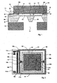
- a sensor has a silicon part 100, formed on a substrate with a rigid support rim 102 and a flexible microstructure which forms a thin flexible diaphragm 104.
- the substrate is heavily doped in order to obtain low series resistance.
- a shallow recess is etched in the diaphragm 104, and the support rim 102 has an electrically insulating layer 107 on the surface thereof.
- a conductive thin film layer 108 is formed on the electrically insulating layer 107 as a ring which surrounds the diaphragm 104.
- a first glass part 120 has a thin-film surface conduction system, formed with metal interconnects, on its surface, which constitutes a plate electrode 121 facing the silicon diaphragm 104.
- the glass 120 is anodically bonded to the conductive thin film layer on the silicon part 100, thereby forming a complete seal ring 108 at the interface 122.
- the plate electrode 121 makes contact with the electrically conductive thin film seal ring 108 via electrical press contacts 109a and 109b.
- the etched recess of the diaphragm 104 provides a sealed cavity 123 within the device.
- the substrate 100 and the glass part 120 form a capacitive sensing device with the plate electrode 121, on the glass 120, acting as the first electrode.
- This electrode is electrically connected to a wire bonding pad 111a, that is outside of the sealed cavity 123, via the press contacts 109a, 109b formed between the electrode 121 and the metal seal ring 108.
- the sealed cavity 123 acts as the electrical isolation gap in the capacitor.
- the flexible diaphragm 104 is the second electrode of the variable capacitor, and is electrically connected via the support rim 102 to an electrical contact pad 111 b outside the sealed cavity.
- Sensing function is provided by a change in capacitance when a force acts on the flexible structure of the diaphragm 104, thereby pressing the diaphragm 104 in the direction towards the plate electrode 121 on the glass, giving a smaller gap 123 in the capacitor.
- insulating layer 107 is formed on a dielectric material and the seal-ring 108 also acts as a conductor to provide electrical contact between the plate electrode 121 on the glass 120 and the wire bonding pad 111 a situated outside the cavity.
- the basic sensing device shown in Figures 1 and 2 comprises a flexible microstructure which can take the form of a thin diaphragm 104.
- pressure acting on the diaphragm 104 presses the diaphragm 104 towards the plate electrode 121, in the form of the thin-film conduction system.
- the gap 112 between the electrodes therefore decreases.
- the sensing device can therefore be used as a pressure sensor to detect changes in air or liquid pressures.
- the sensor of Figures 1 and 2 also includes a resilient centre boss 106, and an electrically insulating mechanical overload protection component 110.
- This component ensures that, under the influence of an extreme change in the parameter being sensed, the component 110 makes contact with the electrode 121 on the glass 120, thereby ensuring the continued electrical isolation of the two electrodes.
- FIG 3 shows another example of the sensing device of the present invention, in the form of a capacitive accelerometer.
- the accelerometer 40 comprises a silicon part 400 built on a substrate 430.
- the silicon part 400 has a rigid support rim 402 joined by a thin, flexible spring to seismic mass 406, such that the mass 406 is supported at the end of the spring.
- the spring and mass constitute a thin, flexible diaphragm 404 which is electrically connected to an electrical contact pad (not shown) through the support rim 402.
- the silicon support rim 402 has an electrically insulating ring-shaped layer 407, the surface of which has an electrically conductive, thin-film layer 408.
- This thin-film layer acts an electrically conductive seal ring 408 which surrounds the diaphragm 404, and is similar to the seal ring 108 of the pressure sensor of Figure 1 .
- a glass part 420 of the capacitor accelerometer 40 has a thin-film conduction system, formed with metal interconnects, on its surface, which faces the silicon part 400.
- the conduction system acts as a plate electrode in use.
- the glass part 420 is anodically bonded to the silicon part 400 in order to form a complete seal at the interface 422 between the two parts.
- the seal-ring 408 has press contact areas 409A, 409B formed between the electrode 421 and the seal ring 408, and is connected to the wire bonding area 411 that is situated outside the capacitive accelerometer, in order to provide an electrical connection out of and/or into the sensing device. Press contacts 409A and 409B form an effective electrical connection between the plate electrode 421 and the thin-film seal ring 408.
- a shallow recess is etched in the thin diaphragm 404 such that, when the glass and silicon parts are connected as described above, a vacuum reference volume, exists between the plate electrode 421 and diaphragm 404.
- a sealed cavity 423 is therefore provided between the glass 420 and the silicon 400 parts of the sensing device. This seal cavity 423 acts as an electrical isolation gap of the capacitive accelerometer.
- the plate electrode 421 and seismic mass 406 of the silicon diaphragm 404 act as the first and second electrodes, respectively, of the capacitive accelerometer 40.
- the accelerometer 40 functions in a similar way to the capacitive pressure sensor 10 described above.
- An acceleration acting on the mass 406 forces the diaphragm 404 to deflect in a direction towards or away from the plate electrode 421, thereby altering the size of the gap 412 between the electrodes, and hence the capacitance value measured.
- an electrically insulating mechanical overload protection component 410 is provided on the diaphragm 404.
- Figures 4 and 5 show alternative configurations for forming the press contacts 109 of the sensing device.
- Figure 4 shows details of a press contact 109 as a individual component which links the metal electrode 121 of the glass 120 to the metal of the seal ring 108.
- Figure 5 the metal of the electrode 121 and that of the seal ring 108, contact one another directly.
- These press contact arrangements use the seal-ring 122 to incorporate the sealing function and electrical contact function into a single component, thereby allowing for a simplified device, with fewer parts. This incorporation also makes the device easier to manufacture.
- FIG. 6 shows a further example of the invention in which a sensing device 20 is connected in series to one or more metal-oxide-semiconductor capacitors (MOS-capacitors) 212a-d via the substrate of the sensor.
- MOS-capacitors metal-oxide-semiconductor capacitors
- the MOS-capacitors should initially have a capacitance value higher than that of the sensor, and have interconnect 213a-d designed with areas which can be removed using a laser beam. By “trimming" the MOS-capacitor in this way, its capacitance value is reduced, and hence the overall capacitance value of the system, is increased.
- the ratio at which the capacitor changes as a function of the detected parameter, the sensitivity of the device can be set at a constant defined value that is not dependent on processing tolerances.
- the electrode pattern on the glass part 320 of the sensor 30 comprises at least two electrodes.
- the electrodes 321 a-h are connected in parallel within the cavity by a metal interconnect system on the glass part, (322a-h) and the silicon part, (323a-d).
- the metal line connecting the top capacitance electrode can be cut through the glass using a laser beam, and the overall capacitance value of the sensor can be reduced.
- Figure 8 illustrates a sequence of the manufacturing process of a device according to the present invention (as illustrated in Figures 1 and 2 ).
- the silicon substrate should be heavily doped via a standard lithographic method, ion implantation and/or high temperature diffusion of dopants.
- the silicon part 100 of the sensor, including the rigid support rim 102 can be manufactured by standard methods well-known within ths field of technology, such as silicon planar processors, double side photolithography, and wet and dry etching techniques.
- the recess is wet and/or dry etched on the silicon in two etching steps. The first of which creates press contacts 109a and 109b, and the second of which creates the recess to provide a gap 112 in the fully manufactured sensor.
- the electrically insulating layer 107 may be thermally grown or vapour deposited on the surface of the rigid support rim 102, and the seal ring 108, in the form of a conductive thin-film layer, may then be formed on top of this.
- the metal plate electrode 121 on the glass part 120 can be made by standard methods for the fabrication of thin-film structures on glass.
- the gap 112 and position of the press contacts 109a and 109b can also be created by etching the recess in the glass 120, or by performing a combination of etching steps in both the glass parts 120 and the silicon part 100.
- Manufacture of this sensing device is completed by anodically bonding, in a vacuum, a glass substrate 120 with metal electrode 121 and thin film interconnects already formed thereon, to the silicon substrate 100, resulting in a structure as shown in Figures 1 and 2 , with the (anodic bonded) seal-ring 108 and the sealed cavity 123 formed by the recesses etched in the surface of the silicon substrate.
Claims (8)
- Capteur de type capacitif comprenant :un substrat (120; 420) en verre, sur lequel est formée une électrode (121; 421) etune structure (100; 400) micro-usinée en un matériau semi-conducteur et comprenant un bord (102; 402) rigide de support ayant un bord (107; 407) isolant qui y est formé etun joint (108; 408) conducteur formé sur le bord (107; 407) isolant et relié au substrat (120; 420) en verre pour définir une cavité (123; 423) enfermée contenant l'électrode (121; 421), en définissant ainsi un élément capacitif,le joint (108; 408) conducteur étant agencé en outre pour relier électriquement l'électrode (121; 421) à un plot (111; 411) de connexion électrique prévu à l'extérieur de la cavité (123; 423) de manière en ce que, en utilisation, un signal électrique puisse y passer pour en déterminer une capacité indicatrice du paramètre à déterminer par le capteur,caractérisé en ce qu'un côté du bord (102; 402) faisant face au substrat (120; 420) en verre comprend un premier étage plus bas et un deuxième étage plus haut, des contacts (109, 109a, 109b; 409a, 409b) par pression étant formés entre le joint (108; 408) conducteur et l'électrode (121; 421) au premier étage plus bas et le substrat (120; 420) en verre étant reliés au joint (108; 408) conducteur au deuxième étage plus haut.
- Capteur suivant la revendication 1, dans lequel la structure micro-usinée comprend un diaphragme (104; 404).
- Capteur suivant la revendication 2, dans lequel un connecteur électrique est prévu aussi sur le diaphragme (104; 404).
- Capteur suivant la revendication 3, dans lequel le connecteur électrique pour le diaphragme (104; 404) est procuré par le matériau semi-conducteur.
- Capteur suivant l'une des revendications 2 à 4, dans lequel le diaphragme (104) comprend un bossage (106) rigide au centre.
- Capteur suivant n'importe quelle revendication précédente, dans lequel le matériau semi-conducteur est du silicium.
- Capteur suivant n'importe quelle revendication précédente, dans lequel la structure (100; 400) à semi-conducteur et le bord (102; 402) rigide de support sont en une pièce unique en matériau semi-conducteur.
- Capteur suivant n'importe quelle revendication précédente, dans lequel le joint entre le substrat (120; 420) en verre et le matériau semi-conducteur est procuré par une liaison anodique.
Priority Applications (3)
| Application Number | Priority Date | Filing Date | Title |
|---|---|---|---|
| EP03256397.5A EP1522521B1 (fr) | 2003-10-10 | 2003-10-10 | Capteur capacitif |
| US10/915,485 US7150195B2 (en) | 2003-10-10 | 2004-08-11 | Sealed capacitive sensor for physical measurements |
| CNA2004100770099A CN1605560A (zh) | 2003-10-10 | 2004-09-09 | 电容传感器 |
Applications Claiming Priority (1)
| Application Number | Priority Date | Filing Date | Title |
|---|---|---|---|
| EP03256397.5A EP1522521B1 (fr) | 2003-10-10 | 2003-10-10 | Capteur capacitif |
Publications (2)
| Publication Number | Publication Date |
|---|---|
| EP1522521A1 EP1522521A1 (fr) | 2005-04-13 |
| EP1522521B1 true EP1522521B1 (fr) | 2015-12-09 |
Family
ID=34307003
Family Applications (1)
| Application Number | Title | Priority Date | Filing Date |
|---|---|---|---|
| EP03256397.5A Expired - Fee Related EP1522521B1 (fr) | 2003-10-10 | 2003-10-10 | Capteur capacitif |
Country Status (3)
| Country | Link |
|---|---|
| US (1) | US7150195B2 (fr) |
| EP (1) | EP1522521B1 (fr) |
| CN (1) | CN1605560A (fr) |
Families Citing this family (62)
| Publication number | Priority date | Publication date | Assignee | Title |
|---|---|---|---|---|
| WO2005001422A2 (fr) * | 2003-06-06 | 2005-01-06 | The Board Of Trustees Of The University Of Illinois | Puce de detection et appareil pour une detection tactile et/ou de flux |
| JP4555612B2 (ja) * | 2004-01-21 | 2010-10-06 | セイコーインスツル株式会社 | 容量型力学量センサ |
| SE0400330D0 (sv) * | 2004-02-12 | 2004-02-12 | Gambro Lundia Ab | Pressure sensing |
| US7644624B2 (en) | 2004-06-04 | 2010-01-12 | The Board Of Trustees Of The University Of Illinois | Artificial lateral line |
| US20060191351A1 (en) * | 2005-02-25 | 2006-08-31 | Meehan Peter G | Sealed capacitive sensor |
| US7622782B2 (en) * | 2005-08-24 | 2009-11-24 | General Electric Company | Pressure sensors and methods of making the same |
| JP4839747B2 (ja) * | 2005-09-20 | 2011-12-21 | 三菱電機株式会社 | 静電容量型加速度センサ |
| US7635077B2 (en) * | 2005-09-27 | 2009-12-22 | Honeywell International Inc. | Method of flip chip mounting pressure sensor dies to substrates and pressure sensors formed thereby |
| US7216547B1 (en) * | 2006-01-06 | 2007-05-15 | Honeywell International Inc. | Pressure sensor with silicon frit bonded cap |
| US7661319B2 (en) * | 2006-06-02 | 2010-02-16 | The Board Of Trustees Of The University Of Illinois | Micromachined artificial haircell |
| JP5092462B2 (ja) * | 2006-06-13 | 2012-12-05 | 株式会社デンソー | 力学量センサ |
| WO2008125130A1 (fr) * | 2007-04-12 | 2008-10-23 | Nokia Corporation | Clavier |
| US7737514B1 (en) * | 2008-02-21 | 2010-06-15 | Yee-Chung Fu | MEMS pressure sensor using area-change capacitive technique |
| US8115265B2 (en) * | 2008-03-26 | 2012-02-14 | Meggitt (San Juan Capistrano), Inc. | Interconnection system on a plane adjacent to a solid-state device structure |
| US8872287B2 (en) * | 2008-03-27 | 2014-10-28 | United Microelectronics Corp. | Integrated structure for MEMS device and semiconductor device and method of fabricating the same |
| ES2341159B1 (es) * | 2008-04-11 | 2011-02-02 | Farsens, S.L. | Proceso de prototipado multiple para microsensores mecanicos de tipo capacitivo. |
| US7851975B2 (en) * | 2008-09-02 | 2010-12-14 | United Microelectronics Corp. | MEMS structure with metal protection rings |
| US8525389B2 (en) | 2008-09-02 | 2013-09-03 | United Microelectronics Corp. | MEMS device with protection rings |
| TWI472472B (zh) * | 2008-09-08 | 2015-02-11 | United Microelectronics Corp | 微機電系統結構及其製造方法 |
| US8334159B1 (en) | 2009-03-30 | 2012-12-18 | Advanced Numicro Systems, Inc. | MEMS pressure sensor using capacitive technique |
| US8072056B2 (en) | 2009-06-10 | 2011-12-06 | Medtronic, Inc. | Apparatus for restricting moisture ingress |
| US8172760B2 (en) | 2009-06-18 | 2012-05-08 | Medtronic, Inc. | Medical device encapsulated within bonded dies |
| TWI372570B (en) * | 2009-12-25 | 2012-09-11 | Ind Tech Res Inst | Capacitive sensor and manufacturing method thereof |
| FR2958748B1 (fr) * | 2010-04-08 | 2012-06-08 | Commissariat Energie Atomique | Dispositif formant capteur de pression, procede de realisation d'un tel capteur et application a la realisation d'un ecran tactile |
| TWI421955B (zh) | 2010-06-30 | 2014-01-01 | 矽品精密工業股份有限公司 | 具壓力感測器之微機電結構及其製法 |
| CN102336390B (zh) * | 2010-07-26 | 2015-07-15 | 矽品精密工业股份有限公司 | 具有压力感测器的微机电结构及其制造方法 |
| DE102010038534A1 (de) * | 2010-07-28 | 2012-02-02 | Robert Bosch Gmbh | Sensorelement zur kapazitiven Differenzdruckmessung |
| US8666505B2 (en) | 2010-10-26 | 2014-03-04 | Medtronic, Inc. | Wafer-scale package including power source |
| US8424388B2 (en) | 2011-01-28 | 2013-04-23 | Medtronic, Inc. | Implantable capacitive pressure sensor apparatus and methods regarding same |
| US8643140B2 (en) | 2011-07-11 | 2014-02-04 | United Microelectronics Corp. | Suspended beam for use in MEMS device |
| US8525354B2 (en) | 2011-10-13 | 2013-09-03 | United Microelectronics Corporation | Bond pad structure and fabricating method thereof |
| US8590389B2 (en) * | 2012-02-10 | 2013-11-26 | Metrodyne Microsystems Corporation, R.O.C. | MEMS pressure sensor device and manufacturing method thereof |
| JP6008393B2 (ja) | 2012-07-28 | 2016-10-19 | 株式会社ワコム | 電磁誘導方式の位置指示器及び電子インクカートリッジ |
| JP6012069B2 (ja) * | 2012-09-13 | 2016-10-25 | 株式会社ワコム | 電磁誘導方式の位置指示器及び電子インクカートリッジ |
| US9249008B2 (en) | 2012-12-20 | 2016-02-02 | Industrial Technology Research Institute | MEMS device with multiple electrodes and fabricating method thereof |
| CN103964370A (zh) * | 2013-01-29 | 2014-08-06 | 北京大学 | 一种电容式压力传感器的制备方法 |
| US8981501B2 (en) | 2013-04-25 | 2015-03-17 | United Microelectronics Corp. | Semiconductor device and method of forming the same |
| FI125960B (en) | 2013-05-28 | 2016-04-29 | Murata Manufacturing Co | Improved pressure gauge box |
| EP3028007A4 (fr) | 2013-08-02 | 2017-07-12 | Motion Engine Inc. | Capteur de mouvement à système microélectromécanique (mems) et procédé de fabrication |
| FI126999B (en) | 2014-01-17 | 2017-09-15 | Murata Manufacturing Co | Improved pressure sensor |
| CN103792036B (zh) * | 2014-03-05 | 2016-01-20 | 中国电子科技集团公司第三十八研究所 | 气压与加速度传感器相集成的mems芯片及其制作方法 |
| US20170030788A1 (en) | 2014-04-10 | 2017-02-02 | Motion Engine Inc. | Mems pressure sensor |
| US11674803B2 (en) | 2014-06-02 | 2023-06-13 | Motion Engine, Inc. | Multi-mass MEMS motion sensor |
| US11111135B2 (en) * | 2014-07-02 | 2021-09-07 | My01 Ip Holdings Inc. | Methods and devices for microelectromechanical pressure sensors |
| TWI513981B (zh) | 2014-11-13 | 2015-12-21 | Ind Tech Res Inst | 具多重氣密空腔的微機電裝置及其製作方法 |
| WO2016090467A1 (fr) | 2014-12-09 | 2016-06-16 | Motion Engine Inc. | Magnétomètre de système micro électromécanique (mems) 3d et procédés associés |
| US10107662B2 (en) | 2015-01-30 | 2018-10-23 | Honeywell International Inc. | Sensor assembly |
| US9967679B2 (en) * | 2015-02-03 | 2018-05-08 | Infineon Technologies Ag | System and method for an integrated transducer and temperature sensor |
| DE102016107059B4 (de) | 2015-07-17 | 2022-12-22 | Infineon Technologies Dresden Gmbh | Integriertes Halbleiterbauelement und Herstellungsverfahren |
| WO2018235415A1 (fr) * | 2017-06-21 | 2018-12-27 | パナソニックIpマネジメント株式会社 | Capteur de quantité physique |
| JP2019128304A (ja) * | 2018-01-26 | 2019-08-01 | セイコーエプソン株式会社 | 物理量センサー、慣性計測ユニット、電子機器、携帯型電子機器、および移動体 |
| US10823631B2 (en) | 2018-04-18 | 2020-11-03 | Rosemount Aerospace Inc. | High temperature capacitive MEMS pressure sensor |
| CN112840676B (zh) | 2018-10-05 | 2022-05-03 | 美商楼氏电子有限公司 | 响应于声学信号来生成电信号的声学换能器和麦克风组件 |
| WO2020072938A1 (fr) | 2018-10-05 | 2020-04-09 | Knowles Electronics, Llc | Procédés de formation de diaphragmes mems comprenant des ondulations |
| DE112019004970T5 (de) | 2018-10-05 | 2021-06-24 | Knowles Electronics, Llc | Mikrofonvorrichtung mit Eindringschutz |
| US11573145B2 (en) * | 2020-03-31 | 2023-02-07 | Rosemount Aerospace Inc. | Capacitive MEMS pressure sensor and method of manufacture |
| CN114530483A (zh) * | 2020-11-23 | 2022-05-24 | 联华电子股份有限公司 | 半导体元件及其制作方法 |
| US11528546B2 (en) | 2021-04-05 | 2022-12-13 | Knowles Electronics, Llc | Sealed vacuum MEMS die |
| US11540048B2 (en) | 2021-04-16 | 2022-12-27 | Knowles Electronics, Llc | Reduced noise MEMS device with force feedback |
| US11649161B2 (en) | 2021-07-26 | 2023-05-16 | Knowles Electronics, Llc | Diaphragm assembly with non-uniform pillar distribution |
| US11772961B2 (en) | 2021-08-26 | 2023-10-03 | Knowles Electronics, Llc | MEMS device with perimeter barometric relief pierce |
| US11780726B2 (en) | 2021-11-03 | 2023-10-10 | Knowles Electronics, Llc | Dual-diaphragm assembly having center constraint |
Citations (1)
| Publication number | Priority date | Publication date | Assignee | Title |
|---|---|---|---|---|
| US5929497A (en) * | 1998-06-11 | 1999-07-27 | Delco Electronics Corporation | Batch processed multi-lead vacuum packaging for integrated sensors and circuits |
Family Cites Families (11)
| Publication number | Priority date | Publication date | Assignee | Title |
|---|---|---|---|---|
| US4426673A (en) * | 1976-03-12 | 1984-01-17 | Kavlico Corporation | Capacitive pressure transducer and method of making same |
| JPS5544786A (en) * | 1978-09-27 | 1980-03-29 | Hitachi Ltd | Pressure sensor |
| US5591679A (en) | 1995-04-12 | 1997-01-07 | Sensonor A/S | Sealed cavity arrangement method |
| US6109113A (en) * | 1998-06-11 | 2000-08-29 | Delco Electronics Corp. | Silicon micromachined capacitive pressure sensor and method of manufacture |
| CA2341182C (fr) * | 1998-08-19 | 2005-01-04 | Wisconsin Alumni Research Foundation | Capteurs de pression capacitifs etanches |
| EP0994330B1 (fr) | 1998-10-12 | 2007-01-03 | Infineon Technologies SensoNor AS | Procédé de fabrication d'un capteur de vitesse angulaire |
| JP3567089B2 (ja) * | 1998-10-12 | 2004-09-15 | 株式会社日立製作所 | 静電容量式圧力センサ |
| US6232150B1 (en) | 1998-12-03 | 2001-05-15 | The Regents Of The University Of Michigan | Process for making microstructures and microstructures made thereby |
| US6449139B1 (en) * | 1999-08-18 | 2002-09-10 | Maxwell Electronic Components Group, Inc. | Multi-electrode double layer capacitor having hermetic electrolyte seal |
| EP1122778A3 (fr) * | 2000-01-31 | 2004-04-07 | Sanyo Electric Co., Ltd. | Dispositif de circuit et son procédé de fabrication |
| US6909178B2 (en) * | 2000-09-06 | 2005-06-21 | Sanyo Electric Co., Ltd. | Semiconductor device and method of manufacturing the same |
-
2003
- 2003-10-10 EP EP03256397.5A patent/EP1522521B1/fr not_active Expired - Fee Related
-
2004
- 2004-08-11 US US10/915,485 patent/US7150195B2/en not_active Expired - Fee Related
- 2004-09-09 CN CNA2004100770099A patent/CN1605560A/zh active Pending
Patent Citations (1)
| Publication number | Priority date | Publication date | Assignee | Title |
|---|---|---|---|---|
| US5929497A (en) * | 1998-06-11 | 1999-07-27 | Delco Electronics Corporation | Batch processed multi-lead vacuum packaging for integrated sensors and circuits |
Also Published As
| Publication number | Publication date |
|---|---|
| EP1522521A1 (fr) | 2005-04-13 |
| US20050076719A1 (en) | 2005-04-14 |
| US7150195B2 (en) | 2006-12-19 |
| CN1605560A (zh) | 2005-04-13 |
Similar Documents
| Publication | Publication Date | Title |
|---|---|---|
| EP1522521B1 (fr) | Capteur capacitif | |
| EP1359402B1 (fr) | Capteur de pression | |
| US7305889B2 (en) | Microelectromechanical system pressure sensor and method for making and using | |
| US7563692B2 (en) | Microelectromechanical system pressure sensor and method for making and using | |
| KR100404904B1 (ko) | 차동 용량형 압력센서 및 그 제조방법 | |
| US8779536B2 (en) | Hybrid integrated pressure sensor component | |
| EP0720731B1 (fr) | Capteur de pression a membranes suspendues | |
| EP1920229B1 (fr) | Capteurs de pression et procedes de realisation | |
| Diem et al. | SOI'SIMOX'; from bulk to surface micromachining, a new age for silicon sensors and actuators | |
| EP1407464B1 (fr) | Capteur micro electromecanique | |
| EP0164413B1 (fr) | Transducteur de pression | |
| US7918136B2 (en) | Micromechanical sensor element | |
| EP3165888B1 (fr) | Capteur de pression à entrefer de détection variable | |
| EP1898196A2 (fr) | Procédé de fabrication d'un capteur de pression capacitif et capteur de pression capacitif fabriqué selon ce procédé | |
| KR20010032103A (ko) | 마이크로-기계적 차압 감응 장치 | |
| CN113428829B (zh) | 一种mems湿压集成传感器及制备方法 | |
| CA2377189A1 (fr) | Dispositifs microelectriques et leurs procedes de fabrication | |
| CN113353883B (zh) | 一种基于相位检测原理的mems压力传感器及制备方法 | |
| Gogoi et al. | Force balanced micromachined pressure sensors | |
| CN117629506A (zh) | 一种复合真空度传感器及其制造方法 | |
| JP2003004566A (ja) | 静電容量型圧力センサ及びその製造方法 | |
| CN113247857A (zh) | 一种高可靠性mems压力传感器结构及封装方法 |
Legal Events
| Date | Code | Title | Description |
|---|---|---|---|
| PUAI | Public reference made under article 153(3) epc to a published international application that has entered the european phase |
Free format text: ORIGINAL CODE: 0009012 |
|
| AK | Designated contracting states |
Kind code of ref document: A1 Designated state(s): AT BE BG CH CY CZ DE DK EE ES FI FR GB GR HU IE IT LI LU MC NL PT RO SE SI SK TR |
|
| AX | Request for extension of the european patent |
Extension state: AL LT LV MK |
|
| 17P | Request for examination filed |
Effective date: 20050930 |
|
| AKX | Designation fees paid |
Designated state(s): DE |
|
| RAP1 | Party data changed (applicant data changed or rights of an application transferred) |
Owner name: INFINEON TECHNOLOGIES SENSONOR AS |
|
| 17Q | First examination report despatched |
Effective date: 20080502 |
|
| RAP1 | Party data changed (applicant data changed or rights of an application transferred) |
Owner name: INFINEON TECHNOLOGIES AG |
|
| REG | Reference to a national code |
Ref country code: DE Ref legal event code: R079 Ref document number: 60348321 Country of ref document: DE Free format text: PREVIOUS MAIN CLASS: B81C0001000000 Ipc: B81B0007000000 |
|
| GRAP | Despatch of communication of intention to grant a patent |
Free format text: ORIGINAL CODE: EPIDOSNIGR1 |
|
| RIC1 | Information provided on ipc code assigned before grant |
Ipc: B81B 7/00 20060101AFI20150505BHEP |
|
| INTG | Intention to grant announced |
Effective date: 20150526 |
|
| GRAS | Grant fee paid |
Free format text: ORIGINAL CODE: EPIDOSNIGR3 |
|
| GRAA | (expected) grant |
Free format text: ORIGINAL CODE: 0009210 |
|
| AK | Designated contracting states |
Kind code of ref document: B1 Designated state(s): DE |
|
| REG | Reference to a national code |
Ref country code: DE Ref legal event code: R096 Ref document number: 60348321 Country of ref document: DE |
|
| REG | Reference to a national code |
Ref country code: DE Ref legal event code: R097 Ref document number: 60348321 Country of ref document: DE |
|
| PLBE | No opposition filed within time limit |
Free format text: ORIGINAL CODE: 0009261 |
|
| STAA | Information on the status of an ep patent application or granted ep patent |
Free format text: STATUS: NO OPPOSITION FILED WITHIN TIME LIMIT |
|
| 26N | No opposition filed |
Effective date: 20160912 |
|
| PGFP | Annual fee paid to national office [announced via postgrant information from national office to epo] |
Ref country code: DE Payment date: 20161220 Year of fee payment: 14 |
|
| REG | Reference to a national code |
Ref country code: DE Ref legal event code: R119 Ref document number: 60348321 Country of ref document: DE |
|
| PG25 | Lapsed in a contracting state [announced via postgrant information from national office to epo] |
Ref country code: DE Free format text: LAPSE BECAUSE OF NON-PAYMENT OF DUE FEES Effective date: 20180501 |