EP1521363A1 - Integrierter Koppler - Google Patents
Integrierter Koppler Download PDFInfo
- Publication number
- EP1521363A1 EP1521363A1 EP04104837A EP04104837A EP1521363A1 EP 1521363 A1 EP1521363 A1 EP 1521363A1 EP 04104837 A EP04104837 A EP 04104837A EP 04104837 A EP04104837 A EP 04104837A EP 1521363 A1 EP1521363 A1 EP 1521363A1
- Authority
- EP
- European Patent Office
- Prior art keywords
- coupler
- junction
- capacitor
- frequency
- series
- Prior art date
- Legal status (The legal status is an assumption and is not a legal conclusion. Google has not performed a legal analysis and makes no representation as to the accuracy of the status listed.)
- Granted
Links
Images

Classifications
-
- H—ELECTRICITY
- H03—ELECTRONIC CIRCUITRY
- H03H—IMPEDANCE NETWORKS, e.g. RESONANT CIRCUITS; RESONATORS
- H03H7/00—Multiple-port networks comprising only passive electrical elements as network components
- H03H7/48—Networks for connecting several sources or loads, working on the same frequency or frequency band, to a common load or source
- H03H7/487—Networks for connecting several sources or loads, working on the same frequency or frequency band, to a common load or source particularly adapted as coupling circuit between transmitters and antennas
Definitions
- the present invention relates to the field of couplers whose function is to take some of the power present on a main line to a secondary line to purposes of control and enslavement.
- Couplers are typically used in gain control systems in closed loop, in order to have a real measure of the power.
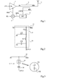
- FIG. 1 represents, very schematically, a example of a conventional circuit using a coupler.
- This example relates to the servo-control of a power amplifier 1 (PA) of amplification of a useful signal UTI to a destination transmission antenna 2.
- PA power amplifier
- a coupler 3 is interposed between the output of the amplifier 1 and the antenna 2 to extract information proportional to the power actually emitted.
- This information is operated by a detector 4 (DET) providing a measured value MES at a comparator 5 with respect to the power required PL.
- the comparator 5 provides a servo signal REG to amplifier 1.
- a first category concerns so-called couplers distributed which are made from transmission lines coupled.
- a second category concerns element couplers localized, based on capacitors and inductors.
- Couplers are directive, that is to say that they detect the meaning of the measured power and are sensitive dimensional variations of the lines. Such couplers are cumbersome because of the size of the lines to be performed, especially for radiofrequency applications (from several hundred MHz to a few GHz).
- Localized element couplers are non-directional. They have the advantage of having a wide bandwidth and being more compact.
- a coupler is defined four ports or terminals IN, DIR, CPLD and ISO.
- IN terminals and DIR are on the main line while CPLD terminals and ISO define the coupled secondary line.
- the IN terminal is power amplifier side 1 while the DIR terminal is antenna side 2.
- the CPLD terminal is the terminal on from which the information proportional to the power in the main line.
- the IN terminals and DIR are merged and the ISO terminal does not generally exist not.
- FIG. 2 shows the electrical diagram of a conventional non-directional coupler with localized elements.
- Such coupler is essentially made up of the association of two cells 31 and 32 constituting respectively pass filters high and low.
- the cell 31 comprises a capacitor C31 whose first electrode is connected to line 12 of transmission (terminals IN and DIR combined) and of which a second electrode is connected by an inductor L31 to ground.
- the second electrode of the capacitor C31 is also a input terminal of the cell 32 formed of an inductor L32 connecting this second electrode to the terminal CPLD, the terminal CPLD being further connected by a capacitor C32 to ground.
- a disadvantage of localized element couplers liabilities such as that illustrated in Figure 2 is related to dispersions (of the order of 20%) of the inductive components and capacitive during their manufacture. Such dispersions find on the parameters of the coupler, which are given for a frequency band of operation.
- the present invention aims at proposing a novel integrable coupler architecture.
- the invention aims more particularly at proposing a non-directive coupler whose parameters are free from scattering problems of localized element couplers classics.
- the invention also aims to allow a fixation easy and accurate values of the coupler components.
- this invention provides a non-directional coupler comprising a semiconductor junction in series with a capacitor, the semiconductor junction being realized so that the frequency threshold below which it has a rectifier behavior is lower than the working frequency of the coupler.
- said semiconductor junction is made in a layer epitaxial whose thickness conditions the threshold frequency at from which the junction does not have a recovery function.
- said capacitor has a value greater than 10 picofarads.
- the semiconductor junction is sized to present, at the coupler's working frequency, a series capacitance the order of a few hundred femtofarads and a resistance series of the order of a few tens of Ohms.
- a feature of the present invention is make an integrated coupler in the form of a junction Semiconductor (PN) in series with a capacitor.
- PN junction Semiconductor
- FIG. 3 represents an embodiment of a coupler 3 according to the present invention.
- a PN 35 junction is connected by a first terminal (indifferently P or N) at the transmission line 12 (terminals IN and DIR confused) while its other terminal is connected to a first electrode of a capacitor 36 whose other electrode defines the CPLD terminal of the coupler.
- the PN junction 35 is used not in recovery element but, at the desired frequencies for the operation of the coupler, to constitute a capacitance 351 in series with a resistor 352 both of very low value.
- Very low value means capacity 351 less than picofarad and 352 resistance less than 100 Ohms.
- the PN junction is thus constructed so as not to straighten the signal at relatively high frequencies (higher at a hundred MHz) of operation selected for the coupler. According to a preferred example, it is carried out with a intrinsic area (PIN diode), for example, in a layer epitaxial.
- the capacitor 36 has the role of blocking the component keep on going. Its value is sufficient to be able to be neglected in the serial association with 351 capacity. preferably, a value greater than 10 picofarads respects these conditions.
- the role of capacitor 36 will be better understood in relationship with the description of Figure 4 incorporating the coupler in its application.
- FIG. 4 represents a coupler 3 according to the invention, shown in the form of a diode 35 in series with a capacitor 36, and whose terminal CPLD is connected to a detection circuit 4 providing a measurement signal MES to destination of a comparator.
- Circuit 4 is a circuit conventional, for example, of the type illustrated in FIG. It comprises a rectifying element 41 (for example, a diode) whose anode is connected to the CPLD terminal and whose cathode is connected, via a capacitor 44, to the mass.
- the cathode of the element 41 is moreover connected, by a resistor 42 to the terminal MES which is connected, by a capacitor 43 to ground.
- Capacitors 43 and 44 form with the resistor 42 a low-pass filter reducing the ripple continuous signal taken from the MES terminal.
- the detector 4 further comprises a circuit of compensated polarization in temperature bringing a level Vdc on the anode of the diode 41.
- This circuit consists of two resistors 45 and 46 in series between an application terminal 47 of the voltage Vdc and the anode of the diode 41. The midpoint of this series association is connected to the ground by a diode 48 in series with a resistor 49.
- Such an assembly makes it possible to obtain an exploitable level even for low powers of signals carried on the main line 12 (less than 0 dBm). Without this polarization, the diode 41 would be blocked for such levels. However, the presence of this tension of polarization requires the use of capacitor 36 so as to avoid a continuous polarization of the PN 35 junction coupler 3 which would cancel the desired operation.
- Figure 5 illustrates an example of integration into a silicon substrate 7 of a PN 35 junction of a coupler according to the invention.
- an epitaxial region 71 is provided between a region P + doped 72 and N + doped substrate 7. This is an example, types of doping that can be reversed.
- a first contact (anode) 73 is taken on region 72 and a second contact (of cathode) 74 is taken on the region N +, that is to say on the substrate 7.
- the PN junction can be made from a bipolar transistor type NPN diode mounted (base and collector connected).
- the threshold frequency fs from which the junction PN no longer corrects the signal depends on the transit time carriers (noted tt). This frequency is proportional to the opposite of the transit time.
- the voltage goes from one negative value to a positive value and vice versa with a periodicity less than the transit time.
- the incursion into direct is too stiff to cause a current and the carrier is evacuated by negative alternation before recombining, therefore before generating a rectified current. It's in this condition that the PN junction is equated with a capacity in series with a resistance.
- the transit time is essentially a function of the thickness of the epitaxial layer and the diffusion coefficient of the carriers. More precisely, the time tt is proportional to W 2 / D, where W represents the thickness of the epitaxial layer and D the diffusion coefficient of the carriers.
- the frequency fs is approximately 1300 / W 2 (fs in MHz and W in ⁇ m).
- the diffusion coefficient D of the carriers can be considered constant. Therefore, the smaller the thickness of the epitaxial layer, the higher the frequency from which the PN junction does not have a rectifying behavior.
- the doping level of the regions intervenes little on the threshold frequency of the PN junction.
- An example of a particular application of the invention relates to couplers used in the field of telephony mobile phone (GSM and DCS).
- GSM and DCS telephony mobile phone
- the value of the 351 capacity is of the order of a few hundred femtofarads.
- This value from the realization of the diode can be adjusted by setting, in according to the desired response and taking into account possible parasitic capacitances, in particular the doping of epitaxy, the active surface, the thickness of the epitaxy in case of complete depletion. Such a value is compatible with frequencies of the order of GHz.
- the resistive element 352 is the order of a few tens of ohms, which is compatible with the realization of a PN junction and, again, adjustable in according to the desired characteristics, by adjusting the gap between the P + and N + regions.
- the anode of the diode thus produced constitutes directly the terminal on which is connected the line 12, that is the antenna and the output of the amplifier power.
- An advantage of a PN junction to realize the coupler is that, in the form of an active coupler, its parameters are controllable even for low capacitance values and resistance, with a much lower dispersion (related to semiconductor technology).
- the "active" coupler becomes therefore integrable. It can then be integrated on the same chip than that of the detection circuit (4, FIG. 4).
- the values to give to resistance 352 and capacity 351 by the conformation of the junction 35 are determined by usual modeling and simulation tools in function of the coupling factor and insertion losses desired and / or acceptable at operating frequencies selected.
- the present invention is capable of various variations and modifications that will appear to man art.
- the practical realization of a diode respecting the constraints given by the invention to form a coupler is within the reach of those skilled in the art from functional and sizing indications given above.
- the invention applies equally well for a lateral diode only for a diode made in a technology vertical and whatever type of diode is made (PN diode, PIN diode, etc.), provided that it is sufficiently slow by relation to the working frequencies sought.
Landscapes
- Transmitters (AREA)
- Semiconductor Integrated Circuits (AREA)
Applications Claiming Priority (2)
| Application Number | Priority Date | Filing Date | Title |
|---|---|---|---|
| FR0350643 | 2003-10-03 | ||
| FR0350643 | 2003-10-03 |
Publications (2)
| Publication Number | Publication Date |
|---|---|
| EP1521363A1 true EP1521363A1 (de) | 2005-04-06 |
| EP1521363B1 EP1521363B1 (de) | 2007-12-12 |
Family
ID=34307564
Family Applications (1)
| Application Number | Title | Priority Date | Filing Date |
|---|---|---|---|
| EP04104837A Not-in-force EP1521363B1 (de) | 2003-10-03 | 2004-10-01 | Integrierter Koppler |
Country Status (4)
| Country | Link |
|---|---|
| US (2) | US7375603B2 (de) |
| EP (1) | EP1521363B1 (de) |
| JP (1) | JP2005167202A (de) |
| DE (1) | DE602004010589D1 (de) |
Cited By (1)
| Publication number | Priority date | Publication date | Assignee | Title |
|---|---|---|---|---|
| US7187062B2 (en) | 2004-04-14 | 2007-03-06 | Avago Technologies Wireless Ip (Singapore) Pte. Ltd. | Coupler detector |
Families Citing this family (9)
| Publication number | Priority date | Publication date | Assignee | Title |
|---|---|---|---|---|
| US7375603B2 (en) * | 2003-10-03 | 2008-05-20 | Stmicroelectronics S.A. | Integrated coupler |
| US7911236B2 (en) * | 2006-11-22 | 2011-03-22 | Intel Mobile Communications GmbH | Detection circuit and detection method |
| JP5279551B2 (ja) * | 2009-03-03 | 2013-09-04 | 三菱電機株式会社 | 半導体スイッチ、半導体スイッチmmic、切り替えスイッチrfモジュール、耐電力スイッチrfモジュールおよび送受信モジュール |
| US8391806B2 (en) | 2011-01-04 | 2013-03-05 | Research In Motion Limited | Wireless communications device with an adjustable impedance matching network and associated methods |
| EP2472728B1 (de) * | 2011-01-04 | 2013-11-27 | BlackBerry Limited | Drahtlose Kommunikationsvorrichtung mit einem einstellbaren Impedanzanpassungsnetzwerk und zugehörige Verfahren |
| US9319006B2 (en) * | 2013-10-01 | 2016-04-19 | Infineon Technologies Ag | System and method for a radio frequency coupler |
| US9322858B2 (en) | 2014-02-04 | 2016-04-26 | Infineon Technologies Austria Ag | System and method for a phase detector |
| JP2018518087A (ja) | 2015-04-17 | 2018-07-05 | バード テクノロジーズ グループ インコーポレイテッド | 無指向性結合器を有する無線周波数電力センサ |
| CN109521496B (zh) * | 2018-12-24 | 2020-09-08 | 广东工业大学 | 基于介质谐振天线的nmosfet太赫兹探测器和方法 |
Citations (4)
| Publication number | Priority date | Publication date | Assignee | Title |
|---|---|---|---|---|
| US3296527A (en) * | 1962-04-12 | 1967-01-03 | Van B Cones | Direct measurement probe for radio frequency energy |
| US4603310A (en) * | 1985-08-20 | 1986-07-29 | The United States Of America As Represented By The Secretary Of The Air Force | T-section digital phase shifter apparatus |
| JPS632404A (ja) * | 1986-06-23 | 1988-01-07 | Kokusai Electric Co Ltd | 誘電体フイルタの帯域幅調整方法 |
| US20020100950A1 (en) * | 2001-01-31 | 2002-08-01 | Babcock Jeffrey A. | P-i-n transit time silicon-on-insulator device |
Family Cites Families (7)
| Publication number | Priority date | Publication date | Assignee | Title |
|---|---|---|---|---|
| US4044373A (en) * | 1967-11-13 | 1977-08-23 | Hitachi, Ltd. | IGFET with gate protection diode and antiparasitic isolation means |
| US4059803A (en) * | 1973-12-13 | 1977-11-22 | Mikhailovsky Leonard Konstanti | Method of converting the electromagnetic spectrum carrier frequency and an electromagnetic energy receiver for same |
| DE3276513D1 (en) * | 1982-11-26 | 1987-07-09 | Ibm | Self-biased resistor structure and application to interface circuits realization |
| US5352994A (en) * | 1987-10-06 | 1994-10-04 | The Board Of Trustees Of The Leland Stanford Junior University | Gallium arsenide monolithically integrated nonlinear transmission line impedance transformer |
| JPH07154169A (ja) * | 1993-11-30 | 1995-06-16 | Matsushita Electric Ind Co Ltd | 高周波電力増幅器 |
| US6660688B2 (en) | 2000-05-31 | 2003-12-09 | Ricoh Company Ltd. | Thermosensitive recording medium |
| US7375603B2 (en) * | 2003-10-03 | 2008-05-20 | Stmicroelectronics S.A. | Integrated coupler |
-
2004
- 2004-09-24 US US10/949,941 patent/US7375603B2/en not_active Expired - Lifetime
- 2004-10-01 EP EP04104837A patent/EP1521363B1/de not_active Not-in-force
- 2004-10-01 JP JP2004289785A patent/JP2005167202A/ja not_active Abandoned
- 2004-10-01 DE DE602004010589T patent/DE602004010589D1/de active Active
-
2008
- 2008-02-22 US US12/035,458 patent/US7760155B2/en not_active Expired - Fee Related
Patent Citations (4)
| Publication number | Priority date | Publication date | Assignee | Title |
|---|---|---|---|---|
| US3296527A (en) * | 1962-04-12 | 1967-01-03 | Van B Cones | Direct measurement probe for radio frequency energy |
| US4603310A (en) * | 1985-08-20 | 1986-07-29 | The United States Of America As Represented By The Secretary Of The Air Force | T-section digital phase shifter apparatus |
| JPS632404A (ja) * | 1986-06-23 | 1988-01-07 | Kokusai Electric Co Ltd | 誘電体フイルタの帯域幅調整方法 |
| US20020100950A1 (en) * | 2001-01-31 | 2002-08-01 | Babcock Jeffrey A. | P-i-n transit time silicon-on-insulator device |
Non-Patent Citations (2)
| Title |
|---|
| PATENT ABSTRACTS OF JAPAN vol. 012, no. 204 (E - 620) 11 June 1988 (1988-06-11) * |
| PATENT ABSTRACTS OF JAPAN vol. 013, no. 195 (E - 754) 10 May 1989 (1989-05-10) * |
Cited By (2)
| Publication number | Priority date | Publication date | Assignee | Title |
|---|---|---|---|---|
| US7187062B2 (en) | 2004-04-14 | 2007-03-06 | Avago Technologies Wireless Ip (Singapore) Pte. Ltd. | Coupler detector |
| GB2413217B (en) * | 2004-04-14 | 2007-09-12 | Agilent Technologies Inc | Coupler detector |
Also Published As
| Publication number | Publication date |
|---|---|
| US20080158090A1 (en) | 2008-07-03 |
| US7375603B2 (en) | 2008-05-20 |
| US20050073373A1 (en) | 2005-04-07 |
| JP2005167202A (ja) | 2005-06-23 |
| US7760155B2 (en) | 2010-07-20 |
| EP1521363B1 (de) | 2007-12-12 |
| DE602004010589D1 (de) | 2008-01-24 |
Similar Documents
| Publication | Publication Date | Title |
|---|---|---|
| US7282692B2 (en) | Light receiving method of an avalanche photodiode and a bias control circuit of the same | |
| EP1521363B1 (de) | Integrierter Koppler | |
| EP3660930A1 (de) | Herstellungsverfahren einer fotodiodenmatrix auf germaniumbasis und mit schwachem dunkelstrom | |
| FR2595007A1 (fr) | Tete de detection optique realisee en optique integree et procede de realisation | |
| EP0836271A1 (de) | Integrierter Oszillator und einen solchen Oszillator verwendendes Funktelefon | |
| EP3706274A1 (de) | Schutzvorrichtung gegen überspannungen | |
| EP1011143B1 (de) | Halbleitervorrichtung mit Substrat vom BiCMOS Typ und Rauschentkopplung | |
| EP0905852A1 (de) | Schutzschaltung mit Filtercharakteristik | |
| EP0737003B1 (de) | Ausleseverstärker für CCD-Register | |
| EP1147389B1 (de) | Bolometrischer detektor mit einer antenne | |
| FR2473811A1 (fr) | Dispositif a onde acoustique de surface | |
| EP0161166B1 (de) | Kompakter Addierer mit Halbleiteranordnungen im Hyperfrequenz-Betrieb | |
| FR2820875A1 (fr) | Structure d'inductance integree | |
| EP0199332B1 (de) | Empfänger für optische Breitbandsignale | |
| FR2849538A1 (fr) | Composant discret comprenant des diodes hf en serie et a cathode commune | |
| EP0241383B1 (de) | Integriertes Tiefpassfilter | |
| JP4045170B2 (ja) | アバランシェフォトダイオードの特性定義方法 | |
| FR2483667A1 (fr) | Dispositif d'echantillonnage et maintien a capacite mos | |
| EP0699359B1 (de) | Vorspannungsstromgesteuerte elektronische schaltung, insbesondere einstellbarer widerstand, negativer widerstand, oder filter oder dergleichen | |
| EP0093086A2 (de) | Bipolare Halbleiteranordnung und MOS-Schaltung mit solch einer Anordnung | |
| FR2780813A1 (fr) | Dispositif a semiconducteur avec isolation inter-element amelioree | |
| EP1229587B1 (de) | Schutzstruktur gegen Störungen | |
| EP0032069B1 (de) | Verfahren zum Einstellen des Temperaturkoeffizienten einer Referenzdiode und so eingestellte Referenzdiode | |
| FR2657202A1 (fr) | Dispositif a onde acoustique de surface et procede pour sa fabrication. | |
| FR3066017B1 (fr) | Dispositif pyroelectrique de detection infrarouge comportant un emetteur infrarouge de modulation |
Legal Events
| Date | Code | Title | Description |
|---|---|---|---|
| PUAI | Public reference made under article 153(3) epc to a published international application that has entered the european phase |
Free format text: ORIGINAL CODE: 0009012 |
|
| AK | Designated contracting states |
Kind code of ref document: A1 Designated state(s): AT BE BG CH CY CZ DE DK EE ES FI FR GB GR HU IE IT LI LU MC NL PL PT RO SE SI SK TR |
|
| AX | Request for extension of the european patent |
Extension state: AL HR LT LV MK |
|
| 17P | Request for examination filed |
Effective date: 20050929 |
|
| AKX | Designation fees paid |
Designated state(s): DE FR GB IT |
|
| GRAP | Despatch of communication of intention to grant a patent |
Free format text: ORIGINAL CODE: EPIDOSNIGR1 |
|
| GRAS | Grant fee paid |
Free format text: ORIGINAL CODE: EPIDOSNIGR3 |
|
| GRAA | (expected) grant |
Free format text: ORIGINAL CODE: 0009210 |
|
| AK | Designated contracting states |
Kind code of ref document: B1 Designated state(s): DE FR GB IT |
|
| REG | Reference to a national code |
Ref country code: GB Ref legal event code: FG4D Free format text: NOT ENGLISH |
|
| REF | Corresponds to: |
Ref document number: 602004010589 Country of ref document: DE Date of ref document: 20080124 Kind code of ref document: P |
|
| GBT | Gb: translation of ep patent filed (gb section 77(6)(a)/1977) |
Effective date: 20080123 |
|
| PLBE | No opposition filed within time limit |
Free format text: ORIGINAL CODE: 0009261 |
|
| STAA | Information on the status of an ep patent application or granted ep patent |
Free format text: STATUS: NO OPPOSITION FILED WITHIN TIME LIMIT |
|
| PG25 | Lapsed in a contracting state [announced via postgrant information from national office to epo] |
Ref country code: DE Free format text: LAPSE BECAUSE OF FAILURE TO SUBMIT A TRANSLATION OF THE DESCRIPTION OR TO PAY THE FEE WITHIN THE PRESCRIBED TIME-LIMIT Effective date: 20080313 |
|
| 26N | No opposition filed |
Effective date: 20080915 |
|
| PGFP | Annual fee paid to national office [announced via postgrant information from national office to epo] |
Ref country code: GB Payment date: 20080926 Year of fee payment: 5 |
|
| REG | Reference to a national code |
Ref country code: FR Ref legal event code: ST Effective date: 20090630 |
|
| PG25 | Lapsed in a contracting state [announced via postgrant information from national office to epo] |
Ref country code: FR Free format text: LAPSE BECAUSE OF NON-PAYMENT OF DUE FEES Effective date: 20081031 |
|
| PG25 | Lapsed in a contracting state [announced via postgrant information from national office to epo] |
Ref country code: GB Free format text: LAPSE BECAUSE OF NON-PAYMENT OF DUE FEES Effective date: 20091001 |
|
| PG25 | Lapsed in a contracting state [announced via postgrant information from national office to epo] |
Ref country code: IT Free format text: LAPSE BECAUSE OF NON-PAYMENT OF DUE FEES Effective date: 20081031 |