EP1521311A2 - Strahlungsemittierender Halbleiterkörper mit Confinement-Schichten - Google Patents
Strahlungsemittierender Halbleiterkörper mit Confinement-Schichten Download PDFInfo
- Publication number
- EP1521311A2 EP1521311A2 EP04022801A EP04022801A EP1521311A2 EP 1521311 A2 EP1521311 A2 EP 1521311A2 EP 04022801 A EP04022801 A EP 04022801A EP 04022801 A EP04022801 A EP 04022801A EP 1521311 A2 EP1521311 A2 EP 1521311A2
- Authority
- EP
- European Patent Office
- Prior art keywords
- radiation
- confinement
- layers
- active layer
- semiconductor body
- Prior art date
- Legal status (The legal status is an assumption and is not a legal conclusion. Google has not performed a legal analysis and makes no representation as to the accuracy of the status listed.)
- Withdrawn
Links
Images

Classifications
-
- H—ELECTRICITY
- H10—SEMICONDUCTOR DEVICES; ELECTRIC SOLID-STATE DEVICES NOT OTHERWISE PROVIDED FOR
- H10H—INORGANIC LIGHT-EMITTING SEMICONDUCTOR DEVICES HAVING POTENTIAL BARRIERS
- H10H20/00—Individual inorganic light-emitting semiconductor devices having potential barriers, e.g. light-emitting diodes [LED]
- H10H20/80—Constructional details
- H10H20/81—Bodies
- H10H20/822—Materials of the light-emitting regions
- H10H20/824—Materials of the light-emitting regions comprising only Group III-V materials, e.g. GaP
-
- H—ELECTRICITY
- H10—SEMICONDUCTOR DEVICES; ELECTRIC SOLID-STATE DEVICES NOT OTHERWISE PROVIDED FOR
- H10H—INORGANIC LIGHT-EMITTING SEMICONDUCTOR DEVICES HAVING POTENTIAL BARRIERS
- H10H20/00—Individual inorganic light-emitting semiconductor devices having potential barriers, e.g. light-emitting diodes [LED]
- H10H20/80—Constructional details
- H10H20/81—Bodies
-
- H—ELECTRICITY
- H10—SEMICONDUCTOR DEVICES; ELECTRIC SOLID-STATE DEVICES NOT OTHERWISE PROVIDED FOR
- H10H—INORGANIC LIGHT-EMITTING SEMICONDUCTOR DEVICES HAVING POTENTIAL BARRIERS
- H10H20/00—Individual inorganic light-emitting semiconductor devices having potential barriers, e.g. light-emitting diodes [LED]
- H10H20/80—Constructional details
- H10H20/81—Bodies
- H10H20/811—Bodies having quantum effect structures or superlattices, e.g. tunnel junctions
- H10H20/812—Bodies having quantum effect structures or superlattices, e.g. tunnel junctions within the light-emitting regions, e.g. having quantum confinement structures
-
- H—ELECTRICITY
- H10—SEMICONDUCTOR DEVICES; ELECTRIC SOLID-STATE DEVICES NOT OTHERWISE PROVIDED FOR
- H10H—INORGANIC LIGHT-EMITTING SEMICONDUCTOR DEVICES HAVING POTENTIAL BARRIERS
- H10H20/00—Individual inorganic light-emitting semiconductor devices having potential barriers, e.g. light-emitting diodes [LED]
- H10H20/80—Constructional details
- H10H20/81—Bodies
- H10H20/822—Materials of the light-emitting regions
-
- H—ELECTRICITY
- H10—SEMICONDUCTOR DEVICES; ELECTRIC SOLID-STATE DEVICES NOT OTHERWISE PROVIDED FOR
- H10H—INORGANIC LIGHT-EMITTING SEMICONDUCTOR DEVICES HAVING POTENTIAL BARRIERS
- H10H20/00—Individual inorganic light-emitting semiconductor devices having potential barriers, e.g. light-emitting diodes [LED]
- H10H20/80—Constructional details
- H10H20/81—Bodies
- H10H20/822—Materials of the light-emitting regions
- H10H20/823—Materials of the light-emitting regions comprising only Group II-VI materials, e.g. ZnO
Definitions
- the invention relates to a radiation-emitting Semiconductor body according to the preamble of patent claim 1 and a radiation-emitting semiconductor body according to the Preamble of claim 6.
- Desirable is as complete as possible Inclusion or a long residence time of the charge carriers in the active layer, since charge carriers outside the active Layer no significant contribution to radiation generation Afford.
- Confinement layers are usually lattice-matched the active layer is executed.
- Lattice matching involves the risk that mechanical Tensions between confinement layer and active Layer as well as defects in the crystal lattice arise. such Defects can degrade the radiation yield as they for example, the non-radiative recombination of Charge carriers.
- the achievable barrier height comparatively low.
- the maximum barrier height is achieved with AlInP confinement layers. Due to the limited barrier height occur in such Semiconductor bodies so-called leakage currents of charge carriers that do not contribute to the generation of radiation.
- a closely related problem of the load carrier inclusion occurs in radiation-emitting quantum well structures InGaAlP based on.
- the inclusion of the charge carriers takes place here in the quantum well or the quantum wells themselves InGaAlP-based quantum well structure has a plurality of successive quantum well and barrier layers.
- the problem occurs here that the height the barrier layers are limited in the case of lattice matching is.
- a radiation-emitting semiconductor body having a radiation-emitting active layer based on In x Al y Ga 1-xy P with 0 ⁇ x ⁇ 1, 0 ⁇ y ⁇ 1, 0 ⁇ x + y ⁇ 1, is disposed between a At least one of the confinement layers In x Al y Ga 1-xy P u N 1-u (InAlGaPN) with 0 ⁇ x ⁇ 1, 0 ⁇ y ⁇ 1, 0 ⁇ x + y ⁇ 1 and 0 ⁇ u ⁇ 1, B z In x Al y Ga 1-xyz P u N 1-u where 0 ⁇ x ⁇ 1, 0 ⁇ y ⁇ 1, 0 ⁇ z ⁇ 1, 0 ⁇ x + y + z ⁇ 1 and 0 ⁇ u ⁇ 1 (BInAlGaPN) or an II-VI semiconductor material, preferably Zn ⁇ Mg 1 -x S y Se 1-y with 0 ⁇ x ⁇ 1 and 0 ⁇ y ⁇ 1 ( Zn
- a confinement layer for an active layer based on InGaAlP be formed, which advantageously a larger Barrier height as an InGaAlP confinement layer, in particular an AlInP confinement layer.
- the confinement layer or are the Confinement layers are lattice-matched.
- the invention with the mentioned Materials for the confinement layers both a sufficiently high barrier height as well as lattice matching the confinement layers to the active layer feasible.
- Grid adaptation of the confinement layers is not mandatory is required. Due to the advantageously large Barrier height of the confinement layers can also be on the Lattice adjustment is dispensed with and a - usually tensile - Tension between active layer and confinement layer be accepted. An increase in the radiation yield can be achieved in this case by the fact that the stress-induced losses due to the improved Inclusion of charge carriers are overcompensated.
- both contain confinement layers in the invention InAlGaPN, BInAlGaPN or II-VI semiconductor material, wherein particularly preferably the first and the second confinement layer has the same composition exhibit.
- the first and the second confinement layer has the same composition exhibit.
- the active layer confinement layers are thus on both sides of the active layer confinement layers with a advantageously provided large barrier height. This leads to an efficient inclusion of the charge carriers or a especially low leakage current.
- the first and / or the second confinement layer in one Spaced from the active layer, which is smaller than the diffusion length is. This is to achieve that the highest possible proportion of those injected into the active layer Charge carriers from inclusion through the confinement layers is detected. Overall, so will the efficiency of Radiation generation further increased.
- a radiation-emitting semiconductor body having a radiation-emitting active layer with a quantum well structure based on In x Al y Ga 1-xy P with 0 ⁇ x ⁇ 1, 0 ⁇ y ⁇ 1, 0 ⁇ x + y ⁇ 1, the barrier layer or at least one of the barrier layers In x Al y Ga 1-xy P u N 1-u with 0 ⁇ x ⁇ 1, 0 ⁇ y ⁇ 1, 0 ⁇ x + y ⁇ 1 and 0 ⁇ u ⁇ 1 and / or B z In x Al y Ga 1-xyz P u N 1-u with 0 ⁇ x ⁇ 1, 0 ⁇ y ⁇ 1, 0 ⁇ z ⁇ 1, 0 ⁇ x + y + z ⁇ 1 and 0 ⁇ u ⁇ 1 or an II-VI semiconductor material.
- InAlGaPN and BInAlGaPN or a II-VI semiconductor material such as Example ZnMgSSe advantageously a larger one Barrier height than with InGaAlP barrier layers and thus a achieve more efficient confinement of the charge carriers, wherein compared to the first embodiment of the Inclusion on the individual quantum wells within the refers to active layer.
- the quantum well or surround the quantum wells on both sides with barrier layers, the InAlGaPN, BInAlGaPN or II-VI semiconductor material contain and prefers the same composition exhibit.
- a further embodiment of the invention consists in a Combination of the first and the second embodiment, so in the case of a radiation-emitting semiconductor body, the active layer a quantum well structure according to the second Embodiment, wherein the active layer on or on both sides of confinement layers after the first Embodiment is surrounded.
- the active layer contain both the barrier layer or Barrier layers of the quantum well structure in the active Layer as well as at least one, preferably both Confinement layers InAlGaPN, BInAlGaPN or an II-VI semiconductor material such as ZnMgSSe.
- the semiconductor body is in the invention as Light emitting diode, for example as LED or laser diode executed.
- the invention can with these components a significant increase in efficiency can be achieved.
- Laser diodes is added that by the invention improved charge trapping the threshold current density can be advantageously reduced.
- the illustrated in Figure 1 first embodiment has a semiconductor body having a substrate 1 on which a Semiconductor layer sequence 7 is applied.
- this Semiconductor layer sequence 7 may, for example, an LED structure will be realized.
- the semiconductor layer sequence 7 comprises a radiation-generating active layer based on InAlGaP.
- the active layer consists of InAlGaP or InAlGaP contains, in the latter case, the active layer may also contain other materials.
- the active layer does not contain a nitride compound semiconductor, ie In x Al y Ga 1-xy P u N 1-u , where 0 ⁇ x ⁇ 1, 0 ⁇ y ⁇ 1, 0 ⁇ x + y ⁇ 1 and 0 ⁇ u ⁇ 1, and in particular consists of one or more layers of InAlGaP.
- the active layer can also be formed in multiple layers with only partial regions of the active layer InAlGaP contained and / or the InAlGaP composition in Subareas of the active layer is different.
- the active layer is lattice-matched on both sides Confinement füren 3,4 downstream, which are preferred directly adjacent to the active layer 2.
- At least one of the two confinement layers contains InAlGaPN, BInAlGaPN or an II-VI semiconductor material such as ZnMgSSe.
- InAlGaPN, BInAlGaPN or a II-VI semiconductor material such as Example ZnMgSSe included, preferably with the same Composition.
- the confinement layers 3,4 not directly to the boundaries are the distance between the confinement layer 3,4 and active layer 2 are preferred in the invention smaller than the diffusion length of the charge carriers in the active layer.
- the diffusion length is a measure of the spatial Staying area of a load carrier during his medium life. At a distance from the active one Layer that is larger than the diffusion length takes the Number of charge carriers injected into the active layer strong. Accordingly, the influence or the efficiency decreases Confinement layers, which are also beneficial increased barrier height only with respect to the remaining Charge carrier can positively affect.
- the illustrated in Figure 2 second embodiment has as the first embodiment with a semiconductor body a substrate 1, on which a semiconductor layer sequence 7 is applied.
- the semiconductor layer sequence 7 comprises again an active radiation generating layer on the Base of InAlGaP and can be used, for example, as a laser structure be executed.
- the active layer 2 is in the second embodiment as a quantum well structure in the form of a Double quantum well structure (DQW, double quantum well) with three Barrier layers 6 and two between each two Barrier layers 6 arranged quantum well layers 8 InGaAlP basis executed.
- DQW Double quantum well structure
- Quantum well structures for example Single quantum well structures or Multiple quantum well structures with more than two Quantum well layers can be provided.
- the barrier layers 6 contain InAlGaPN, BInAlGaPN or an II-VI semiconductor material such as ZnMgSSe. This allows greater barrier heights than conventional InGaAlP barrier layers can be achieved, whereby the Containers and subsequently the efficiency of the Radiation generation is advantageously improved.
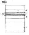
- the third embodiment shown in Figure 3 corresponds to a combination of the first and the second Embodiment.
- the semiconductor body has a substrate 1 with one thereon angeordenten semiconductor layer sequence on.
- the Semiconductor layer sequence comprises as in the first Embodiment one or two InAlGaPN, BInAlGaPN or a confinement layer containing II-VI semiconductor material 3,4, between which the active layer 2 on InGaAlP base is arranged.
- the active layer contains as in the second Embodiment, a quantum well structure 5 with Barrier layers 6 and intermediate InGaAlP-based quantum well layers 8, wherein the Barrier layers 6 InAlGaPN, BInAlGaPN or II-VI semiconductor material contain.
- the barrier height of the confinement layers 3.4 in the third embodiment not the Barrier height of the barrier layers 6 must correspond.
- the barrier height of the Confinement layers 3.4 the barrier height of the Barrier layers surpasses and thus a twofold, staggered charge carrier inclusion is realized.
- the semiconductor layer sequence 7 can also be used in the invention contain additional layers.
- a buffer layer and on the substrate opposite side of the active layer one or more Be arranged contact layers may be arranged between Substrate 1 and active layer 2 or the first confinement layer 3 .
- the active layer or the active layer including the Confinement layers between two mantle or Coating layers may be arranged.
- a substrate is in an inventive Semiconductor body is not mandatory and can be used for Formation of a thin-film component of the Semiconductor layer sequence, which then the semiconductor body represents, be replaced.
- a thin film device Here is a device with a on a growth substrate epitaxially grown Hableiter Anlagenengol to understand, wherein the growth substrate is at least partially of the semiconductor layer sequence is removed.
Landscapes
- Led Devices (AREA)
- Semiconductor Lasers (AREA)
Abstract
Description
Claims (12)
- Strahlungsemittierender Halbleiterkörper mit einer auf InxAlyGa1-x-yP mit 0≤x≤1, 0≤y≤1, 0≤x+y≤1 basierenden strahlungsemittierenden aktiven Schicht (2)
die zwischen einer ersten Confinement-Schicht (3) und einer zweiten Confinement-Schicht (4) angeordnet ist,
dadurch gekennzeichnet, dass
zumindest eine der Confinement-Schichten (3,4) InxAlyGa1-x-yPuN1-u mit 0≤x≤1, 0≤y≤1, 0≤x+y≤1 und 0≤u<1 und/oder BzInxAlyGa1-x-y-zPuN1-u mit 0≤x≤1, 0≤y≤1, 0<z≤1, 0≤x+y+z≤1 und 0≤u<1 oder ein II-VI-Halbleitermaterial enthält. - Strahlungsemittierender Halbleiterträger nach Anspruch 1,
dadurch gekennzeichnet, dass
die Confinement-Schichten (3,4) an die aktive Schicht gitterangepasst sind. - Strahlungsemittierender Halbleiterkörper nach Anspruch 1 oder 2,
dadurch gekennzeichnet, dass
die erste Confinement-Schicht (3) und die zweite Confinement-Schicht (4) InxAlyGa1-x-yPuN1-u mit 0≤x≤1, 0≤y≤1, 0≤x+y≤1 und 0≤u<1, BzInxAlyGa1-x-y-zPuN1-u mit 0≤x≤1, 0≤y≤1, 0<z≤1, 0≤x+y+z≤1 und 0≤u<1 oder ein II-VI-Halbleitermaterial enthalten. - Strahlungsemittierender Halbleiterkörper nach einem der Ansprüche 1 bis 3,
dadurch gekennzeichnet, dass
die Zusammensetzung der ersten und der zweiten Confinement-Schicht (3,4) gleich ist. - Strahlungsemittierender Halbleiterkörper nach einem der Ansprüche 1 bis 4,
dadurch gekennzeichnet, dass
der aktiven Schicht (2) eine Diffusionslänge für die im Betrieb injizierten Ladungsträger zugeordnet ist,
und die erste und/oder die zweite Confinement-Schicht (3,4) in einem Abstand von der aktiven Schicht (2) angeordnet ist, der kleiner ist als die Diffusionlänge. - Strahlungsemittierender Halbleiterkörper mit einer auf InxAlyGa1-x-yP mit 0≤x≤1, 0≤y≤1, 0≤x+y≤1 basierenden strahlungsemittierenden aktiven Schicht (2) mit einer Quantentopfstruktur (5), die eine oder mehrere Barrierenschichten (6) aufweist,
dadurch gekennzeichnet, dass
die Barrierenschicht (6) bzw. mindestens eine der Barrierenschichten (6) InxAlyGa1-x-yPuN1-u mit 0≤x≤1, 0≤y≤1, 0≤x+y≤1 und 0≤u<1 und/oder BzInxAlyGa1-x-y-zPuN1-u mit 0≤x≤1, 0≤y≤1, 0<z≤1, 0≤x+y+z≤1 und 0≤u<1 oder ein II-VI-Halbleitermaterial enthält. - Strahlungsemittierender Halbleiterkörper nach Anspruch 6,
dadurch gekennzeichnet, dass
die Quantentopfstruktur (5) mehrere Barriereschichten (6) mit der gleichen Zusammensetzung aufweist. - Strahlungsemittierender Halbleiterkörper nach Anspruch 6,
dadurch gekennzeichnet, dass
die aktive Schicht (2) zwischen zwei Confinement-Schichten (3,4) gemäß einem der Ansprüche 1 bis 5 angeordnet ist. - Strahlungsemittierender Halbleiterkörper nach einem der Ansprüche 1 bis 8,
dadurch gekennzeichnet, dass
das II-VI-Halbleitermaterial ZnxMg1-xSySe1-y mit 0≤x≤1 und 0≤y≤1 ist. - Strahlungsemittierender Halbleiterkörper nach einem der Ansprüche 1 bis 9,
dadurch gekennzeichnet, dass
gilt: x>0, y>0 und x+y<1. - Strahlungsemittierender Halbleiterkörper nach Anspruch 10,
dadurch gekennzeichnet, dass
gilt: u>0. - Strahlungsemittierender Halbleiterkörper nach einem der Ansprüche 1 bis 11,
dadurch gekennzeichnet, dass
der Halbleiterkörper eine Lichtemissionsdiode, insbesondere eine LED oder eine Laserdiode ist.
Applications Claiming Priority (4)
| Application Number | Priority Date | Filing Date | Title |
|---|---|---|---|
| DE10345412 | 2003-09-30 | ||
| DE10345412 | 2003-09-30 | ||
| DE10355962 | 2003-12-01 | ||
| DE10355962A DE10355962A1 (de) | 2003-09-30 | 2003-12-01 | Strahlungsemittierender Halbleiterkörper mit Confinement-Schichten |
Publications (2)
| Publication Number | Publication Date |
|---|---|
| EP1521311A2 true EP1521311A2 (de) | 2005-04-06 |
| EP1521311A3 EP1521311A3 (de) | 2010-09-15 |
Family
ID=34315000
Family Applications (1)
| Application Number | Title | Priority Date | Filing Date |
|---|---|---|---|
| EP20040022801 Withdrawn EP1521311A3 (de) | 2003-09-30 | 2004-09-24 | Strahlungsemittierender Halbleiterkörper mit Confinement-Schichten |
Country Status (3)
| Country | Link |
|---|---|
| US (1) | US7495249B2 (de) |
| EP (1) | EP1521311A3 (de) |
| JP (1) | JP2005109495A (de) |
Cited By (2)
| Publication number | Priority date | Publication date | Assignee | Title |
|---|---|---|---|---|
| WO2014029633A1 (de) * | 2012-08-23 | 2014-02-27 | Osram Opto Semiconductors Gmbh | Optoelektronischer halbleiterkörper und optoelektronischer halbleiterchip |
| WO2018234153A1 (de) * | 2017-06-20 | 2018-12-27 | Osram Opto Semiconductors Gmbh | Optoelektronischer halbleiterchip und verfahren zum betrieb des optoelektronischen halbleiterchips |
Families Citing this family (1)
| Publication number | Priority date | Publication date | Assignee | Title |
|---|---|---|---|---|
| RU2650606C2 (ru) * | 2016-08-17 | 2018-04-16 | Российская Федерация, от имени которой выступает Федеральное государственное казенное учреждение "Войсковая часть 35533" | ГЕТЕРОСТРУКТУРА GaPAsN СВЕТОДИОДА И ФОТОПРИЕМНИКА НА ПОДЛОЖКЕ Si И СПОСОБ ЕЕ ИЗГОТОВЛЕНИЯ |
Family Cites Families (17)
| Publication number | Priority date | Publication date | Assignee | Title |
|---|---|---|---|---|
| JPH07115243A (ja) | 1993-10-15 | 1995-05-02 | Hitachi Ltd | 半導体レーザ素子 |
| JPH07231142A (ja) * | 1994-02-18 | 1995-08-29 | Mitsubishi Electric Corp | 半導体発光素子 |
| US5670798A (en) * | 1995-03-29 | 1997-09-23 | North Carolina State University | Integrated heterostructures of Group III-V nitride semiconductor materials including epitaxial ohmic contact non-nitride buffer layer and methods of fabricating same |
| JPH0945993A (ja) * | 1995-07-28 | 1997-02-14 | Sony Corp | 半導体発光素子 |
| KR100486803B1 (ko) * | 1996-06-18 | 2005-06-16 | 소니 가부시끼 가이샤 | 자발광표시장치 |
| US6233264B1 (en) * | 1996-08-27 | 2001-05-15 | Ricoh Company, Ltd. | Optical semiconductor device having an active layer containing N |
| US6563850B1 (en) * | 1997-10-06 | 2003-05-13 | Sharp Kabushiki Kaisha | Light-emitting device and fabricating method thereof |
| JP3559453B2 (ja) * | 1998-06-29 | 2004-09-02 | 株式会社東芝 | 発光素子 |
| JP2000183399A (ja) | 1998-12-11 | 2000-06-30 | Furukawa Electric Co Ltd:The | GaN系化合物半導体発光素子 |
| JP2000332362A (ja) * | 1999-05-24 | 2000-11-30 | Sony Corp | 半導体装置および半導体発光素子 |
| US6472679B1 (en) * | 1999-12-31 | 2002-10-29 | Matsushita Electric Industrial Co., Ltd. | Semiconductor structures using a group III-nitride quaternary material system with reduced phase separation and method of fabrication |
| US6448584B1 (en) * | 2000-01-14 | 2002-09-10 | Shih-Hsiung Chan | Light emitting diode with high luminance and method for making the same |
| US6858882B2 (en) * | 2000-09-08 | 2005-02-22 | Sharp Kabushiki Kaisha | Nitride semiconductor light-emitting device and optical device including the same |
| JP4416297B2 (ja) * | 2000-09-08 | 2010-02-17 | シャープ株式会社 | 窒化物半導体発光素子、ならびにそれを使用した発光装置および光ピックアップ装置 |
| JP2002164352A (ja) * | 2000-09-13 | 2002-06-07 | Toshiba Corp | バイポーラトランジスタ、半導体発光素子、及び半導体素子 |
| US6525335B1 (en) * | 2000-11-06 | 2003-02-25 | Lumileds Lighting, U.S., Llc | Light emitting semiconductor devices including wafer bonded heterostructures |
| TW546852B (en) * | 2002-04-15 | 2003-08-11 | Epistar Corp | Mixed-light type LED and the manufacturing method thereof |
-
2004
- 2004-09-24 EP EP20040022801 patent/EP1521311A3/de not_active Withdrawn
- 2004-09-28 JP JP2004281689A patent/JP2005109495A/ja not_active Withdrawn
- 2004-09-30 US US10/956,728 patent/US7495249B2/en not_active Expired - Fee Related
Cited By (3)
| Publication number | Priority date | Publication date | Assignee | Title |
|---|---|---|---|---|
| WO2014029633A1 (de) * | 2012-08-23 | 2014-02-27 | Osram Opto Semiconductors Gmbh | Optoelektronischer halbleiterkörper und optoelektronischer halbleiterchip |
| US9306114B2 (en) | 2012-08-23 | 2016-04-05 | Osram Opto Semiconductors Gmbh | III-V compound semiconductor-based-light-emitting diode device with embedded charge carrier barrier |
| WO2018234153A1 (de) * | 2017-06-20 | 2018-12-27 | Osram Opto Semiconductors Gmbh | Optoelektronischer halbleiterchip und verfahren zum betrieb des optoelektronischen halbleiterchips |
Also Published As
| Publication number | Publication date |
|---|---|
| JP2005109495A (ja) | 2005-04-21 |
| US20050074044A1 (en) | 2005-04-07 |
| EP1521311A3 (de) | 2010-09-15 |
| US7495249B2 (en) | 2009-02-24 |
Similar Documents
| Publication | Publication Date | Title |
|---|---|---|
| EP1883141B1 (de) | LD oder LED mit Übergitter-Mantelschicht | |
| DE112004001447B4 (de) | Nitridhalbleiter-Licht-emittierende Einrichtung | |
| EP2208240B1 (de) | Optoelektronischer halbleiterchip mit einer mehrfachquantentopfstruktur | |
| DE102011112706B4 (de) | Optoelektronisches Bauelement | |
| EP1883140A1 (de) | LD oder LED mit Übergitter-Mantelschicht und Dotierungsgradienten | |
| EP3206238B1 (de) | Lichtemittierende dünnfilm-diode mit einer spiegelschicht und verfahren zu deren herstellung | |
| WO2018050466A1 (de) | Halbleiterschichtenfolge | |
| DE102013105707A1 (de) | Halbleitervorrichtung, Übergitterschicht, welche in derselben verwendet wird, und Verfahren zur Herstellung der Halbleitervorrichtung | |
| DE112012005796T5 (de) | Photoaktive Bauelemente mit einer verbesserten Verteilung von Ladungsträgern sowie Verfahren zum Ausbilden derselben | |
| DE102007044439A1 (de) | Optoelektronischer Halbleiterchip mit Quantentopfstruktur | |
| EP1883119B1 (de) | Halbleiter-Schichtstruktur mit Übergitter | |
| EP3345224B1 (de) | Optoelektronischer halbleiterchip und verfahren zu dessen herstellung | |
| EP2235759B1 (de) | Optoelektronisches bauelement und verfahren zur herstellung eines optoelektronischen bauelements | |
| DE102009037416B4 (de) | Elektrisch gepumpter optoelektronischer Halbleiterchip | |
| WO2021013740A1 (de) | Optoelektronischer halbleiterchip | |
| DE102006046237A1 (de) | Halbleiter-Schichtstruktur mit Übergitter | |
| DE112023000394T5 (de) | Mikrohalbleiter-leuchtdioden-struktur und verfahren zu deren herstellung | |
| DE102017113585A1 (de) | Halbleiterschichtenfolge und Verfahren zur Herstellung einer Halbleiterschichtenfolge | |
| DE112005000703B4 (de) | Licht-emittierende Einrichtung und Herstellungsverfahren derselben | |
| WO2013034486A1 (de) | Optoelektronisches bauelement | |
| DE10203393B4 (de) | Halbleiterbauelement mit einem Halbleiterkörper auf der Basis eines Nitrid-Verbindungshalbleiters | |
| DE102024127908A1 (de) | Lichtemittierendes element vom typ nitrid-halbleiter | |
| DE102019133214A1 (de) | Strahlungsemittierender Halbleiterchip | |
| WO2014173950A1 (de) | Optoelekronisches gan-basiertes bauelement mit erhöhter esd resistenz durch ein übergitter und verfahren zu seiner herstellung | |
| DE102008010296A1 (de) | LED mit Stromaufweitungsschicht |
Legal Events
| Date | Code | Title | Description |
|---|---|---|---|
| PUAI | Public reference made under article 153(3) epc to a published international application that has entered the european phase |
Free format text: ORIGINAL CODE: 0009012 |
|
| AK | Designated contracting states |
Kind code of ref document: A2 Designated state(s): AT BE BG CH CY CZ DE DK EE ES FI FR GB GR HU IE IT LI LU MC NL PL PT RO SE SI SK TR |
|
| AX | Request for extension of the european patent |
Extension state: AL HR LT LV MK |
|
| RAP1 | Party data changed (applicant data changed or rights of an application transferred) |
Owner name: OSRAM OPTO SEMICONDUCTORS GMBH |
|
| RAP1 | Party data changed (applicant data changed or rights of an application transferred) |
Owner name: OSRAM OPTO SEMICONDUCTORS GMBH |
|
| PUAL | Search report despatched |
Free format text: ORIGINAL CODE: 0009013 |
|
| AK | Designated contracting states |
Kind code of ref document: A3 Designated state(s): AT BE BG CH CY CZ DE DK EE ES FI FR GB GR HU IE IT LI LU MC NL PL PT RO SE SI SK TR |
|
| AX | Request for extension of the european patent |
Extension state: AL HR LT LV MK |
|
| 17P | Request for examination filed |
Effective date: 20110221 |
|
| AKX | Designation fees paid |
Designated state(s): DE FR GB |
|
| 17Q | First examination report despatched |
Effective date: 20110429 |
|
| STAA | Information on the status of an ep patent application or granted ep patent |
Free format text: STATUS: THE APPLICATION IS DEEMED TO BE WITHDRAWN |
|
| 18D | Application deemed to be withdrawn |
Effective date: 20150724 |