EP1521306A2 - Bipolartransistor und dessen Herstellungsverfahren - Google Patents
Bipolartransistor und dessen Herstellungsverfahren Download PDFInfo
- Publication number
- EP1521306A2 EP1521306A2 EP04255999A EP04255999A EP1521306A2 EP 1521306 A2 EP1521306 A2 EP 1521306A2 EP 04255999 A EP04255999 A EP 04255999A EP 04255999 A EP04255999 A EP 04255999A EP 1521306 A2 EP1521306 A2 EP 1521306A2
- Authority
- EP
- European Patent Office
- Prior art keywords
- emitter
- opening
- forming
- substrate
- bipolar junction
- Prior art date
- Legal status (The legal status is an assumption and is not a legal conclusion. Google has not performed a legal analysis and makes no representation as to the accuracy of the status listed.)
- Pending
Links
Images


Classifications
-
- H—ELECTRICITY
- H10—SEMICONDUCTOR DEVICES; ELECTRIC SOLID-STATE DEVICES NOT OTHERWISE PROVIDED FOR
- H10D—INORGANIC ELECTRIC SEMICONDUCTOR DEVICES
- H10D10/00—Bipolar junction transistors [BJT]
-
- H—ELECTRICITY
- H10—SEMICONDUCTOR DEVICES; ELECTRIC SOLID-STATE DEVICES NOT OTHERWISE PROVIDED FOR
- H10D—INORGANIC ELECTRIC SEMICONDUCTOR DEVICES
- H10D10/00—Bipolar junction transistors [BJT]
- H10D10/01—Manufacture or treatment
- H10D10/021—Manufacture or treatment of heterojunction BJTs [HBT]
-
- H—ELECTRICITY
- H10—SEMICONDUCTOR DEVICES; ELECTRIC SOLID-STATE DEVICES NOT OTHERWISE PROVIDED FOR
- H10D—INORGANIC ELECTRIC SEMICONDUCTOR DEVICES
- H10D10/00—Bipolar junction transistors [BJT]
- H10D10/01—Manufacture or treatment
- H10D10/051—Manufacture or treatment of vertical BJTs
-
- H—ELECTRICITY
- H10—SEMICONDUCTOR DEVICES; ELECTRIC SOLID-STATE DEVICES NOT OTHERWISE PROVIDED FOR
- H10D—INORGANIC ELECTRIC SEMICONDUCTOR DEVICES
- H10D10/00—Bipolar junction transistors [BJT]
- H10D10/01—Manufacture or treatment
- H10D10/051—Manufacture or treatment of vertical BJTs
- H10D10/054—Forming extrinsic base regions on silicon substrate after insulating device isolation in vertical BJTs having single crystalline emitter, collector or base regions
-
- H—ELECTRICITY
- H10—SEMICONDUCTOR DEVICES; ELECTRIC SOLID-STATE DEVICES NOT OTHERWISE PROVIDED FOR
- H10D—INORGANIC ELECTRIC SEMICONDUCTOR DEVICES
- H10D10/00—Bipolar junction transistors [BJT]
- H10D10/40—Vertical BJTs
- H10D10/421—Vertical BJTs having both emitter-base and base-collector junctions ending at the same surface of the body
-
- H—ELECTRICITY
- H10—SEMICONDUCTOR DEVICES; ELECTRIC SOLID-STATE DEVICES NOT OTHERWISE PROVIDED FOR
- H10D—INORGANIC ELECTRIC SEMICONDUCTOR DEVICES
- H10D10/00—Bipolar junction transistors [BJT]
- H10D10/80—Heterojunction BJTs
- H10D10/821—Vertical heterojunction BJTs
- H10D10/891—Vertical heterojunction BJTs comprising lattice-mismatched active layers, e.g. SiGe strained-layer transistors
-
- H—ELECTRICITY
- H10—SEMICONDUCTOR DEVICES; ELECTRIC SOLID-STATE DEVICES NOT OTHERWISE PROVIDED FOR
- H10D—INORGANIC ELECTRIC SEMICONDUCTOR DEVICES
- H10D62/00—Semiconductor bodies, or regions thereof, of devices having potential barriers
- H10D62/10—Shapes, relative sizes or dispositions of the regions of the semiconductor bodies; Shapes of the semiconductor bodies
- H10D62/13—Semiconductor regions connected to electrodes carrying current to be rectified, amplified or switched, e.g. source or drain regions
- H10D62/133—Emitter regions of BJTs
-
- H—ELECTRICITY
- H10—SEMICONDUCTOR DEVICES; ELECTRIC SOLID-STATE DEVICES NOT OTHERWISE PROVIDED FOR
- H10D—INORGANIC ELECTRIC SEMICONDUCTOR DEVICES
- H10D84/00—Integrated devices formed in or on semiconductor substrates that comprise only semiconducting layers, e.g. on Si wafers or on GaAs-on-Si wafers
- H10D84/01—Manufacture or treatment
- H10D84/0107—Integrating at least one component covered by H10D12/00 or H10D30/00 with at least one component covered by H10D8/00, H10D10/00 or H10D18/00, e.g. integrating IGFETs with BJTs
- H10D84/0109—Integrating at least one component covered by H10D12/00 or H10D30/00 with at least one component covered by H10D8/00, H10D10/00 or H10D18/00, e.g. integrating IGFETs with BJTs the at least one component covered by H10D12/00 or H10D30/00 being a MOS device
-
- H—ELECTRICITY
- H10—SEMICONDUCTOR DEVICES; ELECTRIC SOLID-STATE DEVICES NOT OTHERWISE PROVIDED FOR
- H10D—INORGANIC ELECTRIC SEMICONDUCTOR DEVICES
- H10D84/00—Integrated devices formed in or on semiconductor substrates that comprise only semiconducting layers, e.g. on Si wafers or on GaAs-on-Si wafers
- H10D84/01—Manufacture or treatment
- H10D84/02—Manufacture or treatment characterised by using material-based technologies
- H10D84/03—Manufacture or treatment characterised by using material-based technologies using Group IV technology, e.g. silicon technology or silicon-carbide [SiC] technology
- H10D84/038—Manufacture or treatment characterised by using material-based technologies using Group IV technology, e.g. silicon technology or silicon-carbide [SiC] technology using silicon technology, e.g. SiGe
-
- H—ELECTRICITY
- H10—SEMICONDUCTOR DEVICES; ELECTRIC SOLID-STATE DEVICES NOT OTHERWISE PROVIDED FOR
- H10D—INORGANIC ELECTRIC SEMICONDUCTOR DEVICES
- H10D84/00—Integrated devices formed in or on semiconductor substrates that comprise only semiconducting layers, e.g. on Si wafers or on GaAs-on-Si wafers
- H10D84/40—Integrated devices formed in or on semiconductor substrates that comprise only semiconducting layers, e.g. on Si wafers or on GaAs-on-Si wafers characterised by the integration of at least one component covered by groups H10D12/00 or H10D30/00 with at least one component covered by groups H10D10/00 or H10D18/00, e.g. integration of IGFETs with BJTs
- H10D84/401—Combinations of FETs or IGBTs with BJTs
Definitions
- This invention relates generally to bipolar transistors, and more specifically to a process for forming an emitter region of a bipolar transistor and a transistor formed according to such a process.
- a bipolar junction transistor comprises three adjacent doped semiconductor regions or layers having an NPN or PNP doping configuration.
- a middle region forms a base and two end regions form an emitter and a collector.
- the emitter has a higher dopant concentration than the base and the collector, and the base has a higher dopant concentration than the collector.
- the BJT can be operated as an amplifier (for example, to amplify an input signal supplied between the base and the emitter, with the output signal appearing across the emitter/collector) or as a switch (for example, an input signal applied across the base/emitter switches the emitter/collector circuit to an opened or a closed (i.e., short-circuited) state.
- the simplest structure is a planar architecture with stacked NPN or PNP regions formed by successive dopant implantations into a substrate.
- Significant performance enhancements are achieved by forming the emitter from a single layer of polysilicon. For example, using a polysilicon emitter allows greater control over the emitter-base doping profile.
- a second significant enhancement can be achieved by using two layers of polysilicon, one for the emitter and the other for an extrinsic base region. This architecture reduces base resistance and collector-base capacitance, among other advantages.
- the emitter polysilicon layer deposits in an emitter window
- the polysilicon deposits on both the bottom surface and sidewalls of the window.
- the bottom window surface is formed by the base region, and thus the polysilicon deposited on the bottom surface forms a base/emitter junction.
- the polysilicon formed on the bottom window surface tends to be thinner than a fully deposited layer thickness due to a pinch-off condition caused as polysilicon is deposited on window sidewalls, interfering with polysilicon deposition on the window bottom surface. If the polysilicon material on the bottom window surface material is too thin, the bipolar junction transistor may not function properly. As emitter window width is reduced to achieve higher transistor operating speeds, the problem of emitter polysilicon window pinch-off is exacerbated.
- the single polysilicon layer process (also referred to as an implanted base process) avoids certain of these disadvantages.
- the masking, patterning and etching steps required to form the base and the emitter can also involve complicated process steps that are prone to produce devices that do not function properly.
- the window pinch-off problem is also observed during deposition of the polysilicon layer in the emitter window.
- An embodiment of the present invention comprises a process for forming an emitter of a bipolar junction transistor.
- the process comprises providing a substrate having a base therein, forming a material layer overlying the substrate, forming an opening in the material layer exposing the base and selectively depositing the emitter within the opening.
- a structure according to the present invention comprises a substrate, a collector disposed in the substrate, an intrinsic base overlying the collector, an extrinsic base laterally adjacent the intrinsic base, a dielectric layer overlying the intrinsic base, wherein an opening is defined in the dielectric layer and an emitter in the opening, wherein the emitter is confined to the opening.
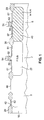
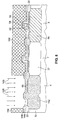
- Figures 1-7 are cross-sectional illustrations of sequential processing steps for forming a bipolar junction transistor and metal-oxide semiconductor field effect transistors according to a first method of the present invention.
- Figures 8-14 are cross-sectional illustrations of sequential processing steps for forming a bipolar junction transistor and metal-oxide semiconductor field effect transistors according to a second method of the prior art.
- the emitter polysilicon for the BJT is deposited only where required during a selective deposition process.
- the emitter silicon can be deposited in a conventional selective silicon deposition system using HCl (hydrochloric acid).
- selective deposition can be achieved in a system that advantageously utilizes the time lag between the start of silicon growth on a clean silicon surface and the start of silicon growth on a silicon dioxide or a silicon nitride surface.
- a process sequence for forming a selectively deposited emitter for a NPN bipolar junction transistor architecture, according to the teachings of the present invention, and further comprising an implanted base, is described below in conjunction with the Figures 1-10, which show cross-sectional views of the formed structures according to sequential processing steps.
- the illustrated prior art process is a BiCMOS process, wherein bipolar transistors and CMOS (complimentary metal oxide semiconductor field effect transistors) are formed on a substrate.
- CMOS complementary metal oxide semiconductor field effect transistors
- the illustrated exemplary process employs LOCOS (local oxidation of silicon) isolation.
- the LOCOS regions are formed by first oxidizing the p-type silicon substrate 10 (see Figure 1) to form a silicon dioxide layer, also referred to as a pad oxide layer.
- a silicon nitride layer (not shown) is deposited overlying the silicon dioxide layer.
- the silicon nitride layer and the silicon dioxide layer are etched according to an overlying patterned photoresist layer to form openings therein.
- the remaining regions form an oxidation mask for subsequent LOCOS oxidation, permitting oxidation of the substrate 10 only through openings in the silicon nitride and silicon dioxide layers.
- the LOCOS oxidation process forms isolation silicon dioxide regions 20 as illustrated in Figure 1.
- the remaining regions of the silicon nitride and the silicon dioxide layers are chemically stripped and a sacrificial silicon dioxide layer is formed over the substrate 10 in regions between adjacent isolation regions 20.
- isolation structures such as shallow and deep trench isolation structures, can be used alone or in combination with other isolation structures.
- a photoresist layer is deposited, masked, patterned and developed to form a p-tub photoresist implant mask (not shown).
- a p-type dopant is implanted through the mask to form a p-tub 27 in the NMOS region 7 of the substrate 10. See Figure 1.
- n-tub photoresist implant mask is formed and n-type dopants implanted through the mask, forming an n-tub 40 in the PMOS region 8 and a collector region 42 for an NPN BJT device.
- the collector region 42 serves as a sinker region for connecting to a subsequently formed subcollector (as described below in conjunction with Figure 2).
- a wet clean process removes the n-tub photoresist mask and the sacrificial silicon dioxide layer.
- a silicon dioxide layer, a polysilicon layer and a tungsten silicide layer are blanket deposited on an upper surface 46 of the substrate 10.
- the polysilicon layer is doped through an implant mask, and the layers are patterned to form the gate stack layers.
- the resulting gate stack structure comprises gate oxide regions 50, polysilicon regions 52 and tungsten silicide regions 54 over each of the p-tub 27 (in the NMOS region 7) and the n-tub 40 (in the PMOS region 8).
- n-type lightly doped drain regions 61 are formed in the p-tub 27 and an n-type lightly doped collector contact region 62 is formed in the BJT region 6.
- p-type lightly doped drain regions 67 are formed in the n-tub 40.
- a TEOS (tetraethylorthosilicate) silicon dioxide layer 68 is formed overlying the substrate 10. See Figure 2.
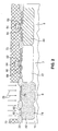
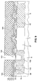
- a subcollector mask 72 Using a subcollector mask 72, a subcollector 74 is implanted (as represented by n-type implant arrowheads 76) in the BJT region 6. After forming the subcollector 74, a p-type base 75 is formed over the subcollector 74 by implant counterdoping using a p-type dopant.
- a spacer silicon dioxide layer 80 is deposited over the substrate 10.
- the layer 80 is formed by a TEOS process.
- a relatively thin amorphous silicon layer 82 is deposited over the silicon dioxide layer 80 to serve as a mask for a subsequent wet etch step.
- the amorphous silicon layer 82 and the underlying silicon dioxide layer 80 are anisotropically etched to form an emitter window 91. The etch process stops on the TEOS layer 68, which is removed from the emitter window 91, as shown, during a subsequent wet etch process.
- a polysilicon layer (not shown) is blanket deposited (including within the emitter window 91) for use in forming the BJT emitter.
- the polysilicon layer is implanted (or doped in-situ) with arsenic or another n-type dopant.
- a silicon emitter 250 is selectively deposited in the emitter window 91 on a surface 252 (silicon) of the base 75. See also the close-up view illustrated in Figure 5.
- selective deposition is meant the deposition of silicon on bare silicon, but not on silicon dioxide or silicon nitride.
- the selective silicon deposition is performed in a hydrochloric acid (HCl) atmosphere (in one embodiment), permitting the deposition of silicon only in regions where bare silicon is exposed, such as the silicon surface 252 of the base 75.
- HCl hydrochloric acid
- the silicon grows across the entire substrate 10, but the silicon etch rate on the dielectric surfaces is faster than the growth rate on those dielectric surfaces.
- the silicon is selectively deposited only on the silicon surfaces.
- the emitter formed according to the teachings of the present invention can be doped in-situ or implanted after deposition.
- a mask is formed to prevent dopant implants in regions of the substrate 10 other than the emitter 250.
- a mask may be unnecessary, depending on the thickness of the silicon dioxide layer 82 overlying the substrate 10, which may form a suitable mask for the implant step.
- the deposition and patterning of the emitter 250 occur in the same process step.
- the prior art process steps associated with etching the blanket polysilicon layer are thus not required to form the emitter.
- Gate stack spacers 100 for the PMOSFET and NMOSFET devices are formed by removing the layer 82, and anisotropically etching the silicon dioxide layer 80. During this etching process, the TEOS silicon dioxide layer 68 is also removed. See the resulting structure illustrated in Figure 6.
- a photoresist layer is deposited and patterned to form an n+ source/drain mask for implanting a high dose (n+) of arsenic into the p-tub 27, forming a source 106 and a drain 108 for the NMOS region 6. See Figure 7.
- Arsenic is also implanted into the BJT collector region 42 through the same mask, forming an n+ ohmic collector contact region 110 with a relatively high doping level to minimize contact resistance with a subsequently-formed overlying collector contact.
- FIG. 10 illustrates the final device appearance, prior to deposition of a dielectric layer overlying the substrate and additional dielectric layers disposed between metallization layers for interconnecting the doped regions formed in the substrate 10.
- FIG. 8-14 show cross-sectional views of the formed structures according to sequential processing steps.
- the illustrated process is a BiCMOS process, wherein bipolar transistors and CMOS (complimentary metal oxide semiconductor field effect transistors) are formed on a substrate.
- CMOS complementary metal oxide semiconductor field effect transistors
- the teachings of the present invention can also be applied to formation of BJT's on a substrate without the formation of CMOS transistors on the same substrate.
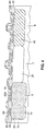
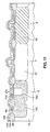
- Figure 8 illustrates a subcollector 142 formed by n-type implant doping through a suitably patterned mask (not shown).
- a TEOS spacer oxide layer 144 and a polysilicon layer 146 are formed on the substrate 10.
- the polysilicon layer 146 is doped with a high-dose implant of boron (represented by implant arrowheads 148) through an implant mask 150.
- the boron implanted polysilicon layer 146 will form an extrinsic base region as described below.
- a silicon nitride layer 156 and a silicon dioxide layer 158 are deposited over the polysilicon layer 146.
- a photoresist layer 160 is deposited and patterned to form a window 162 therein.
- the silicon dioxide layer 158, the silicon nitride layer 156 and the polysilicon layer 146 are anisotropically etched through the window 162, stopping on the TEOS layer 144, to form an emitter window 163 in the substrate 10.
- a collector region 166 is implanted through the window 162.
- a layer of silicon nitride is deposited and anisotropically etched to form sidewall spacers 170. See Figure 10.
- a wet etch process removes the silicon dioxide TEOS layers 68 and 144 from within the emitter window 163, forming a primary cavity 174 and cavities 175 laterally disposed relative to the primary cavity 174.
- An intrinsic base and a cap region are formed in the cavities 174 and 175 during a silicon-germanium epitaxial growth step.
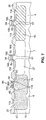
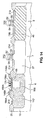
- a silicon nitride spacer 180 and an underlying silicon dioxide (TEOS) spacer 182 are formed in the window 163 as illustrated in the close-up view of Figure 12.
- the spacers which serve to increase the space between a later-formed n+ emitter and a p+ extrinsic base, are formed by depositing a TEOS silicon dioxide layer and a silicon nitride layer. The layers are anisotropically etched back to form the spacers 180 and 182, with the etch stopping on a region of the TEOS layer formed on an upper surface of the intrinsic base and cap region 176. In another embodiment the spacers 180 and 182 may not be required as the previously formed spacers 170 are sufficient. Following spacer formation, the remaining region of the TEOS silicon dioxide layer overlying the upper surface of the intrinsic base and cap region 173 is removed by a wet etch process.
- an emitter 260 is deposited selectively in a hydrochloric acid (HCl) atmosphere (in one embodiment) as described above, permitting the deposition of silicon only on a silicon surface 262 of the intrinsic base 176.
- the emitter can be doped in-situ or implanted after deposition.
- the implant step may be accomplished either masked or unmasked, depending on the thickness of the silicon nitride layer 156 overlying the base polysilicon layer 146. That is, if the silicon nitride layer 156 is sufficiently thick to block the implanted dopants in all regions except in the emitter 260, then a mask layer may not be necessary.
- the BiCMOS process continues by using a patterned hard mask or photoresist mask to etch the polysilicon layer 146, forming extrinsic base regions 146A.
- processing of the BJT is essentially complete.
- the BJT comprises (as shown in Figure 13) the intrinsic base 176, the extrinsic base regions 146A (formed from doped polysilicon), the selectively deposited emitter 260 and the collector regions 42, 142 and 66.
- a spacer etch step anisotropically etches the TEOS layer 144 and the silicon nitride layer 156 to form spacers 202 for the gate stack.
- n-type impurity is implanted through an appropriately patterned mask to form source/drain regions 214 and a collector contact 213. See Figure 14.
- a p-type impurity is implanted in the n-tub 40 to form source/drain regions 218.
- Figure 14 illustrates a preferred final configuration of the various elements prior to deposition of the first dielectric layer and the first metallization interconnect layer.
- windows are defined in the first dielectric layer and conductive plugs formed therein for establishing electrical contact with the various regions of the BJT and the two MOSFET's.
- Interconnect structures for connecting the regions are formed in the first metallization layer. Additional alternating dielectric layers and interconnect layers are formed over the first metallization layer to complete the interconnect system of the integrated circuit.
- an emitter formed according to the teachings of the present invention is formed of single-crystalline or polycrystalline material.
- the material crystalline structure is dependent on the growth conditions, growth surface cleaning techniques and other process parameters. Both the single-crystalline and the polycrystalline emitter embodiments are acceptable.
- the width of the emitter window can be significantly reduced, compared to the prior art, without the resulting adverse window-narrowing effects encountered when the emitter is formed from a deposited polysilicon layer.
- a BJT formed according to the present invention can provide a higher operating speed by using a narrower emitter window.
- the emitter polysilicon layer is absent, the overall height of the BJT structure is reduced as compared with a prior art BJT.
- the thick silicon nitride insulating layer 156 which is etched to form the silicon nitride region 156A (see Figure 13) between the extrinsic base region 146A and the emitter is not required for reducing the base/emitter capacitance. Also, the thickness of the lowest dielectric layer on which the conductive interconnects are formed is reduced.
- this invention ameliorates the so-called "plug effect", where the arsenic n-type dopant concentration disadvantageously varies at the emitter-base interface due to thickness variations in the prior art emitter polysilicon layer across the emitter window 91.
- the profile of the selectively-deposited emitter (250 or 260), according to the teachings of the present invention does not cause the large thickness variations, thus avoiding the "plug effect.”
- the emitter grows on the bottom and side surfaces of the opening, creating an emitter that may be thinner on the opening bottom surface than on the side surfaces.
- the material forming on the side surfaces can converge, "pinching off” the deposition process and creating a void between the pinched off region and the opening base.
- Such an improperly formed emitter can impair operation of the BJT due to the lack of sufficient emitter material in contact with the base region.
- This disadvantage is avoided according to the teachings of the present invention as the emitter fills the opening from the bottom during the selective deposition process.
Landscapes
- Bipolar Transistors (AREA)
- Metal-Oxide And Bipolar Metal-Oxide Semiconductor Integrated Circuits (AREA)
- Bipolar Integrated Circuits (AREA)
- Electrodes Of Semiconductors (AREA)
Applications Claiming Priority (2)
| Application Number | Priority Date | Filing Date | Title |
|---|---|---|---|
| US50737403P | 2003-09-30 | 2003-09-30 | |
| US507374P | 2003-09-30 |
Publications (1)
| Publication Number | Publication Date |
|---|---|
| EP1521306A2 true EP1521306A2 (de) | 2005-04-06 |
Family
ID=34312474
Family Applications (1)
| Application Number | Title | Priority Date | Filing Date |
|---|---|---|---|
| EP04255999A Pending EP1521306A2 (de) | 2003-09-30 | 2004-09-29 | Bipolartransistor und dessen Herstellungsverfahren |
Country Status (5)
| Country | Link |
|---|---|
| US (1) | US20050098852A1 (de) |
| EP (1) | EP1521306A2 (de) |
| JP (1) | JP2005109501A (de) |
| KR (1) | KR20050032014A (de) |
| TW (1) | TW200518341A (de) |
Families Citing this family (5)
| Publication number | Priority date | Publication date | Assignee | Title |
|---|---|---|---|---|
| KR100731087B1 (ko) * | 2005-10-28 | 2007-06-22 | 동부일렉트로닉스 주식회사 | 바이씨모스 소자 및 그의 제조방법 |
| US20070278539A1 (en) * | 2006-06-02 | 2007-12-06 | Agere Systems Inc. | Junction field effect transistor and method for manufacture |
| US7572708B1 (en) | 2007-03-08 | 2009-08-11 | National Semiconductor Corporation | Utilization of doped glass on the sidewall of the emitter window in a bipolar transistor structure |
| CN110660811A (zh) | 2018-06-28 | 2020-01-07 | 联华电子股份有限公司 | 半导体结构及其制造方法 |
| US11094599B2 (en) | 2018-06-28 | 2021-08-17 | United Microelectronics Corp. | Semiconductor structure and manufacturing method thereof |
Family Cites Families (17)
| Publication number | Priority date | Publication date | Assignee | Title |
|---|---|---|---|---|
| JPS63107167A (ja) * | 1986-10-24 | 1988-05-12 | Oki Electric Ind Co Ltd | 半導体集積回路装置の製造方法 |
| US5059544A (en) * | 1988-07-14 | 1991-10-22 | International Business Machines Corp. | Method of forming bipolar transistor having self-aligned emitter-base using selective and non-selective epitaxy |
| US4988632A (en) * | 1990-01-02 | 1991-01-29 | Motorola, Inc. | Bipolar process using selective silicon deposition |
| JP2531355B2 (ja) * | 1993-06-30 | 1996-09-04 | 日本電気株式会社 | バイポ―ラトランジスタおよびその製造方法 |
| JP2746225B2 (ja) * | 1995-10-16 | 1998-05-06 | 日本電気株式会社 | 半導体装置及びその製造方法 |
| US5773350A (en) * | 1997-01-28 | 1998-06-30 | National Semiconductor Corporation | Method for forming a self-aligned bipolar junction transistor with silicide extrinsic base contacts and selective epitaxial grown intrinsic base |
| US6248650B1 (en) * | 1997-12-23 | 2001-06-19 | Texas Instruments Incorporated | Self-aligned BJT emitter contact |
| US6020246A (en) * | 1998-03-13 | 2000-02-01 | National Semiconductor Corporation | Forming a self-aligned epitaxial base bipolar transistor |
| US6359317B1 (en) * | 1998-12-28 | 2002-03-19 | Agere Systems Guardian Corp. | Vertical PNP bipolar transistor and its method of fabrication |
| FR2799048B1 (fr) * | 1999-09-23 | 2003-02-21 | St Microelectronics Sa | Procede de fabrication d'un transistor bipolaire vertical auto-aligne |
| FR2805923B1 (fr) * | 2000-03-06 | 2002-05-24 | St Microelectronics Sa | Procede de fabrication d'un transistor bipolaire double- polysilicium auto-aligne |
| FR2806831B1 (fr) * | 2000-03-27 | 2003-09-19 | St Microelectronics Sa | Procede de fabrication d'un transistor bipolaire de type double-polysilicium auto-aligne a base a heterojonction et transistor correspondant |
| TW472394B (en) * | 2000-05-03 | 2002-01-11 | Ind Tech Res Inst | A bipolar transistor process with epitaxial base |
| US6495904B1 (en) * | 2000-08-23 | 2002-12-17 | National Semiconductor Corporation | Compact bipolar transistor structure |
| US6492237B2 (en) * | 2001-02-12 | 2002-12-10 | Maxim Integrated Products, Inc. | Method of forming an NPN device |
| US6617619B1 (en) * | 2002-02-04 | 2003-09-09 | Newport Fab, Llc | Structure for a selective epitaxial HBT emitter |
| US6586307B1 (en) * | 2002-02-14 | 2003-07-01 | Newport Fab, Llc | Method for controlling an emitter window opening in an HBT and related structure |
-
2004
- 2004-09-29 EP EP04255999A patent/EP1521306A2/de active Pending
- 2004-09-29 JP JP2004283339A patent/JP2005109501A/ja active Pending
- 2004-09-29 US US10/953,476 patent/US20050098852A1/en not_active Abandoned
- 2004-09-29 TW TW093129462A patent/TW200518341A/zh unknown
- 2004-09-30 KR KR1020040078077A patent/KR20050032014A/ko not_active Withdrawn
Also Published As
| Publication number | Publication date |
|---|---|
| KR20050032014A (ko) | 2005-04-06 |
| TW200518341A (en) | 2005-06-01 |
| JP2005109501A (ja) | 2005-04-21 |
| US20050098852A1 (en) | 2005-05-12 |
Similar Documents
| Publication | Publication Date | Title |
|---|---|---|
| US7871869B2 (en) | Extremely-thin silicon-on-insulator transistor with raised source/drain | |
| US6261915B1 (en) | Process of making polysilicon resistor | |
| JPH0744232B2 (ja) | Bi―CMOSデバイス製造方法 | |
| JPH0677421A (ja) | トランジスタの製法 | |
| US20030176033A1 (en) | Disposable spacer technology for reduced cost CMOS processing | |
| EP0694963B1 (de) | Eine Methode zur Herstellung von BiCMOS-Halbleiterteilen | |
| US8084313B2 (en) | Method for forming a bipolar junction transistor and a metal oxide semiconductor field effect transistor | |
| JPH09504411A (ja) | セルフアラインcmosプロセス | |
| EP1273036B1 (de) | Verfahren zur herstellung einer heteroübergang-bicmos-integrierter schaltung | |
| US7863148B2 (en) | Method for integrating SiGe NPN and vertical PNP devices | |
| EP0768709A2 (de) | BiCMOS-Verfahren mit Bipolartransistor mit geringem Basis-Rekombinationsstrom | |
| EP0518611A2 (de) | Verfahren zur Herstellung einer Halbleiterstruktur mit MOS- und Bipolar-Bauteilen | |
| US5057455A (en) | Formation of integrated circuit electrodes | |
| EP1521306A2 (de) | Bipolartransistor und dessen Herstellungsverfahren | |
| US20070161173A1 (en) | Process to integrate fabrication of bipolar devices into a CMOS process flow | |
| JP3638313B2 (ja) | 併合された装置を支援するBiCMOS処理工程 | |
| EP0656660B1 (de) | BiCMOS-Verfahren | |
| CN101313394B (zh) | 制造半导体器件的方法以及用该方法获得的半导体器件 | |
| JP2718257B2 (ja) | 集積回路における埋込み層容量の減少 | |
| EP0942467A1 (de) | Herstellungsverfahren für bipolare und BiCMOS Bauelemente | |
| JP2697631B2 (ja) | 半導体装置の製造方法 | |
| JP3956879B2 (ja) | 半導体集積回路装置の製造方法 | |
| JPH08162632A (ja) | 半導体装置およびその製造方法 | |
| JPH05175219A (ja) | 半導体装置とその製造方法 | |
| JP2006173258A (ja) | 半導体装置の製造方法 |
Legal Events
| Date | Code | Title | Description |
|---|---|---|---|
| PUAI | Public reference made under article 153(3) epc to a published international application that has entered the european phase |
Free format text: ORIGINAL CODE: 0009012 |
|
| AK | Designated contracting states |
Kind code of ref document: A2 Designated state(s): AT BE BG CH CY CZ DE DK EE ES FI FR GB GR HU IE IT LI LU MC NL PL PT RO SE SI SK TR |
|
| AX | Request for extension of the european patent |
Extension state: AL HR LT LV MK |
|
| RIN1 | Information on inventor provided before grant (corrected) |
Inventor name: JONES ROBERT FRANCIS Inventor name: RUSSEL WILLIAM A. Inventor name: CHEN ALAN SANGONE Inventor name: KERR DANIEL CHARLES Inventor name: CARROLL, MICHAEL SCOTT |
|
| PUAL | Search report despatched |
Free format text: ORIGINAL CODE: 0009013 |
|
| PUAF | Information related to the publication of a search report (a3 document) modified or deleted |
Free format text: ORIGINAL CODE: 0009199SEPU |
|
| AK | Designated contracting states |
Kind code of ref document: A3 Designated state(s): AT BE BG CH CY CZ DE DK EE ES FI FR GB GR HU IE IT LI LU MC NL PL PT RO SE SI SK TR |
|
| AX | Request for extension of the european patent |
Extension state: AL HR LT LV MK |
|
| D17D | Deferred search report published (deleted) | ||
| 18W | Application withdrawn |
Effective date: 20060619 |
|
| STAA | Information on the status of an ep patent application or granted ep patent |
Free format text: STATUS: THE APPLICATION HAS BEEN WITHDRAWN |
|
| D18W | Application withdrawn (deleted) | ||
| R18W | Application withdrawn (corrected) |
Effective date: 20060619 |