EP1520457B1 - Abschirmeinrichtung für elektronische baugruppen auf einer leiterplatte - Google Patents
Abschirmeinrichtung für elektronische baugruppen auf einer leiterplatte Download PDFInfo
- Publication number
- EP1520457B1 EP1520457B1 EP03718802A EP03718802A EP1520457B1 EP 1520457 B1 EP1520457 B1 EP 1520457B1 EP 03718802 A EP03718802 A EP 03718802A EP 03718802 A EP03718802 A EP 03718802A EP 1520457 B1 EP1520457 B1 EP 1520457B1
- Authority
- EP
- European Patent Office
- Prior art keywords
- screening
- circuit board
- printed circuit
- screening device
- embodied
- Prior art date
- Legal status (The legal status is an assumption and is not a legal conclusion. Google has not performed a legal analysis and makes no representation as to the accuracy of the status listed.)
- Expired - Lifetime
Links
- 238000012216 screening Methods 0.000 title claims description 32
- 238000007789 sealing Methods 0.000 claims description 17
- 239000000463 material Substances 0.000 claims description 8
- 239000000853 adhesive Substances 0.000 claims description 4
- 230000001070 adhesive effect Effects 0.000 claims description 4
- 239000004952 Polyamide Substances 0.000 claims description 3
- 229910000831 Steel Inorganic materials 0.000 claims description 3
- 229920002647 polyamide Polymers 0.000 claims description 3
- 239000010959 steel Substances 0.000 claims description 3
- 239000007769 metal material Substances 0.000 claims description 2
- RYGMFSIKBFXOCR-UHFFFAOYSA-N Copper Chemical compound [Cu] RYGMFSIKBFXOCR-UHFFFAOYSA-N 0.000 claims 1
- 229910052802 copper Inorganic materials 0.000 claims 1
- 239000010949 copper Substances 0.000 claims 1
- 229920001971 elastomer Polymers 0.000 claims 1
- 239000000806 elastomer Substances 0.000 claims 1
- 239000002861 polymer material Substances 0.000 claims 1
- 238000004519 manufacturing process Methods 0.000 description 10
- 238000005452 bending Methods 0.000 description 6
- 230000000712 assembly Effects 0.000 description 4
- 238000000429 assembly Methods 0.000 description 4
- 239000003566 sealing material Substances 0.000 description 4
- 230000006835 compression Effects 0.000 description 3
- 238000007906 compression Methods 0.000 description 3
- 230000007797 corrosion Effects 0.000 description 3
- 238000005260 corrosion Methods 0.000 description 3
- 230000000694 effects Effects 0.000 description 3
- 239000002184 metal Substances 0.000 description 3
- 230000005855 radiation Effects 0.000 description 3
- 239000005028 tinplate Substances 0.000 description 3
- 239000004020 conductor Substances 0.000 description 2
- 230000005670 electromagnetic radiation Effects 0.000 description 2
- 238000004049 embossing Methods 0.000 description 2
- 238000005516 engineering process Methods 0.000 description 2
- 230000002349 favourable effect Effects 0.000 description 2
- 238000009434 installation Methods 0.000 description 2
- 230000000149 penetrating effect Effects 0.000 description 2
- 230000002093 peripheral effect Effects 0.000 description 2
- 239000004033 plastic Substances 0.000 description 2
- 239000011358 absorbing material Substances 0.000 description 1
- 230000006978 adaptation Effects 0.000 description 1
- 230000002238 attenuated effect Effects 0.000 description 1
- 239000002131 composite material Substances 0.000 description 1
- 238000010276 construction Methods 0.000 description 1
- 238000001816 cooling Methods 0.000 description 1
- 238000013016 damping Methods 0.000 description 1
- 230000001419 dependent effect Effects 0.000 description 1
- 230000000779 depleting effect Effects 0.000 description 1
- 239000000428 dust Substances 0.000 description 1
- 230000005489 elastic deformation Effects 0.000 description 1
- 239000013013 elastic material Substances 0.000 description 1
- 238000004870 electrical engineering Methods 0.000 description 1
- 238000005530 etching Methods 0.000 description 1
- 239000000835 fiber Substances 0.000 description 1
- 239000006260 foam Substances 0.000 description 1
- 230000001771 impaired effect Effects 0.000 description 1
- 238000000034 method Methods 0.000 description 1
- 239000000203 mixture Substances 0.000 description 1
- 239000002245 particle Substances 0.000 description 1
- 238000002360 preparation method Methods 0.000 description 1
- 238000003825 pressing Methods 0.000 description 1
- 239000011265 semifinished product Substances 0.000 description 1
- 230000035939 shock Effects 0.000 description 1
- 238000005476 soldering Methods 0.000 description 1
- 238000007711 solidification Methods 0.000 description 1
- 230000008023 solidification Effects 0.000 description 1
- 238000001228 spectrum Methods 0.000 description 1
- 230000001629 suppression Effects 0.000 description 1
- 238000009423 ventilation Methods 0.000 description 1
Images

Classifications
-
- H—ELECTRICITY
- H05—ELECTRIC TECHNIQUES NOT OTHERWISE PROVIDED FOR
- H05K—PRINTED CIRCUITS; CASINGS OR CONSTRUCTIONAL DETAILS OF ELECTRIC APPARATUS; MANUFACTURE OF ASSEMBLAGES OF ELECTRICAL COMPONENTS
- H05K9/00—Screening of apparatus or components against electric or magnetic fields
- H05K9/0007—Casings
- H05K9/002—Casings with localised screening
- H05K9/0022—Casings with localised screening of components mounted on printed circuit boards [PCB]
- H05K9/0024—Shield cases mounted on a PCB, e.g. cans or caps or conformal shields
- H05K9/0026—Shield cases mounted on a PCB, e.g. cans or caps or conformal shields integrally formed from metal sheet
- H05K9/0028—Shield cases mounted on a PCB, e.g. cans or caps or conformal shields integrally formed from metal sheet with retainers or specific soldering features
-
- H—ELECTRICITY
- H05—ELECTRIC TECHNIQUES NOT OTHERWISE PROVIDED FOR
- H05K—PRINTED CIRCUITS; CASINGS OR CONSTRUCTIONAL DETAILS OF ELECTRIC APPARATUS; MANUFACTURE OF ASSEMBLAGES OF ELECTRICAL COMPONENTS
- H05K9/00—Screening of apparatus or components against electric or magnetic fields
- H05K9/0007—Casings
- H05K9/0015—Gaskets or seals
-
- H—ELECTRICITY
- H05—ELECTRIC TECHNIQUES NOT OTHERWISE PROVIDED FOR
- H05K—PRINTED CIRCUITS; CASINGS OR CONSTRUCTIONAL DETAILS OF ELECTRIC APPARATUS; MANUFACTURE OF ASSEMBLAGES OF ELECTRICAL COMPONENTS
- H05K9/00—Screening of apparatus or components against electric or magnetic fields
- H05K9/0007—Casings
- H05K9/002—Casings with localised screening
- H05K9/0022—Casings with localised screening of components mounted on printed circuit boards [PCB]
- H05K9/0024—Shield cases mounted on a PCB, e.g. cans or caps or conformal shields
- H05K9/003—Shield cases mounted on a PCB, e.g. cans or caps or conformal shields made from non-conductive materials comprising an electro-conductive coating
Definitions
- the invention relates to a shielding device with a shield cap which covers an electronic circuit arranged on a printed circuit board, with an edge, which is spaced from a component side of the printed circuit board by a gap, with a contact device which is arranged in the gap and an electrical connection between the Shielding cap and a conductive contour on the circuit board manufactures, wherein at the edge of the shield cap tabs are formed by the shield cap fixed on the circuit board and the contact device is held under elastic bias.
- interference suppression screen housings which dampen the radiation or the radiation of electromagnetic interference.
- the disturbing radiation can also be caused by assemblies that are themselves on the circuit board.
- miniaturized assemblies such as assemblies, which are built in SMD technology, susceptible well and source of interference are often in the immediate vicinity.
- multi-part shields are used in small construction.
- a one-piece, metallic shield, which can be plugged onto a printed circuit board, is known from DE 29 808 620 U1.
- the attachment is made by latching hooks, which engage behind the circuit board on the back.
- the ground contact of the screen with the circuit board is formed by a plurality of resilient tabs. These lobes are at a mounted shielding trough under elastic bias and make the electrical contact by a line or point contact. Under harsh operating conditions, sections of the contacting may fail due to mechanical effects or corrosion. In this case, the shielding efficiency of the suppressor is impaired.
- Another disadvantage is that during assembly of the shield to overcome the spring force of the individual tabs, a contact force is required, which must be applied to the shielding trough and absorbed by the circuit board.
- the shielding effect depends on the contacting spring force and the distance between the individual contact points. But if a large number of resilient lobes must be elastically deformed, a correspondingly high contact pressure is required and it may happen in miniaturized assemblies that the circuit board is deformed inadmissible. Microcracks can form on the conductor structure. Also in the case of the shielding known from DE 297 13 412 U1, the contacting is produced by contact springs revolving around the edge of the umbrella.
- the invention is based on the object to further develop a shielding of the type mentioned in that the shielding efficiency is improved and the production, in particular the production of different sized shielding that shield only partial areas on the circuit board, with less effort is possible.
- the contact device is formed by a circumferentially arranged in the gap sealing body, wherein the sealing body is made of an elastic, electromagnetic wave absorbing material.
- Characteristic of the invention Therefore, therefore, that the contact does not take place, by a plurality of contact points with line or point contact, but by a flat adjacent sealing body made of an elastic material. Due to its compressibility, it adapts better to bulges and unevenness of the printed circuit board. Even with mechanical shock or vibration, a low ohmic contact resistance of the ground contact remains.
- the circumferential in the joint sealing body between shield and printed circuit board sealingly and in this way additionally provides protection against penetrating into the interior of the shield pollution.
- the production tool of the shield is simpler. Setup costs for changes to the production tool are lower.
- the shield can be inexpensively mass produced as a stamped and bent part made of sheet metal.
- the sealing body may be a blank or a semi-finished product. Overall, an adaptation of the production to a partial shielding of different sized areas can be realized on a printed circuit board with less effort.
- each end of a tab may be formed as a Schränklappen.
- the shielding cap is formed of the same material and integrally merging into one another from a metallic material, for example from tinplate.
- the tinplate can be protected by tinning.
- the edge is formed as a right-angled fold, which extends in the mounted state of the shield substantially parallel to the component side and each tab is formed on the outer peripheral side and run off in the course of a wall of the shield.
- the shielding cap can be produced in a stamping and bending process.
- a very effective shielding can be realized by the sealing body is formed as a flat gasket and is secured by an electrically conductive adhesive on the edge of the shield or the component side of the circuit board.
- there is the advantage that when mounting the shield together with seal as a part is manageable.
- the conductive contour of the printed circuit board has a dome-shaped contact point, which presses into the flat gasket. Its surface is sealed by the elastic flat gasket and largely protected against corrosion.
- the shielding cap is formed in a cuboid shape with respect to the geometry to be shielded in the grid dimension of the printed circuit board. This uniformly modular design reduces manufacturing and logistics costs.
- the shield is provided on a ceiling part and / or on a wall part with openings that form passage for cooling air.
- the size of the openings is adapted to the frequency spectrum to be shielded.
- EMC materials can be used to further reduce costs, these are polymeric materials, particularly preferably polyamide nonwoven, which is metallically coated or knit by a metal mesh.
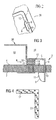
- FIG. 1 an embodiment of the shielding device 1 according to the invention is shown in a perspective exploded view in Figure 1 by way of example.
- the shielding device 1 consists of a shielding cap 20 and of a contact device 6.
- the shielding cap 20 covers in the example shown the entire area of the printed circuit board 2 from.
- the following explanations are not limited to this embodiment, but grasp In particular, shielding the shield only partial areas on the circuit board.
- tabs 8 are formed on the outer peripheral side on the edge 3 of the screening cap 20, by which means the screening cap 20 can be secured on a component side 4 of the printed circuit board 2.
- a conductive contour 7 can be seen, the outline corresponds to the edge region of the shield 20.
- the conductive contour 7 consists of contact points, which are explained in more detail below, and is produced in etching technology in the grid.
- the contact device 6 is designed as a circumferential seal 22.
- the elastic sealing body 22 is pressed first.
- the pressing requires only a slight contact force due to the good compression properties of the sealing material.
- a further lowering causes each end piece 9 of the tab 8 passes through the passage opening and projects beyond the rear.
- the outlet flaps projecting from the passage opening are plastically deformed by a mutual bending. It arises between the cap 20 and the carrier 2 a positive connection.
- the plastic deformation can also be done by bending, by embossing, or by upsetting.
- penetrating electromagnetic radiation energy is greatly attenuated during the passage due to the damping material properties of the sealing material.
- the shielding hood is shown in its longitudinal side with two, in its broad side with an integrally formed fastening tabs.
- the number of fastening tabs varies according to the size of the shielding cap.
- the openings 15 for the loading and ventilation of the interior are drawn greatly enlarged. In reality, the diameter of these holes is very small and tuned to the frequency of the alternating field to be shielded.
- the shielding cap 20 is a one-piece bending stamped part of a tinned tinplate.
- the edge region of the screening cap is drawn in an enlarged detail.
- the edge 3 of the shielding cap 20 is continued by a right-angled fold 12.
- the tab 8 is integrally formed on the fold 12.
- the end portion 9 of the tab 8 is designed as a slanting flaps 11.
- the tab 8 is inserted through the passage opening 10 of the circuit board 2.
- the end portion 9 is plastically deformed by mutual bending about an axis pointing in the direction of passage.
- the cover flap 11 engages behind the back of the printed circuit board 2.
- the circumferential seal 22 simultaneously protects the interior 18 from dust or dirt entering from the outside space 19.
- the seal 22 is drawn as a flat gasket 13. It is in the sealing gap 5 between the printed circuit board 2 and edge 12 under elastic bias.
- the flat gasket 13 is coated on an upper side with an adhesive 14, whereby seal and shield in the Assembly form a unit and are easier to handle.
- the underside of the flat gasket 13 lies along the conductive contour 7 on the component side 4.
- the conductive contour 7 is formed by dome-shaped contact points 21, which are electrically connected via a corresponding layout. Due to the pressure in the sealing gap 5, an elastic deformation of the sealing material occurs.
- the contact points 21 press against the underside of the flat gasket. By this wrapping the tip surface, the contact point is very well protected from external influences. Corrosion in the contacting area is thereby counteracted.
- the contour 7 can also be formed by a continuous conductor track or by another contact pattern.
- the arrangement of the dome-shaped contact points 21 along the conductive contour 7 is shown enlarged in Figure 4 in a plan view.
- the contact points 21 are arranged offset in space.
- the distance of the contact points seen in the longitudinal extent of the ground contact is in the example four millimeters.
- the crests at the contact points are tinned and have a diameter of 1.3 millimeters.
- the EMC flat gasket consists of a polyamide spunbond nonwoven, which has a high compression capacity of up to 85 percent and is very flexible.
- the EMC seal can also be constructed differently and consist of other materials.
- the seal may be, for example, an open-cell foam, the electric and magnetically conductive particles are added. Also suitable are nonwoven and composite materials containing fibers of a material having this conductivity property.
- the metal mesh may be a tinned, copper-clad steel wire mesh.
- the sealing body can be wound on the steel mesh. But it is also possible that the metallic mesh is embedded by polymeric solidification in the sealing body.
Landscapes
- Engineering & Computer Science (AREA)
- Microelectronics & Electronic Packaging (AREA)
- Shielding Devices Or Components To Electric Or Magnetic Fields (AREA)
- Details Of Aerials (AREA)
Description
- Die Erfindung betrifft eine Abschirmeinrichtung mit einer Abschirmkappe, die eine auf einer Leiterplatte angeordnete elektronische Schaltung abdeckt, mit einem Rand, der von einer Bestückungsseite der Leiterplatte durch einen Spalt beabstandet ist, mit einer Kontakteinrichtung, die im Spalt angeordnet ist und eine elektrische Verbindung zwischen der Abschirmkappe und einer leitenden Kontur auf der Leiterplatte herstellt, wobei am Rand der Abschirmkappe Laschen angeformt sind, durch die die Abschirmkappe auf der Leiterplatte festgelegt und die Kontakteinrichtung unter elastischer Vorspannung gehalten ist.
- In der Elektrotechnik ist es häufig erforderlich, elektrische oder magnetische Felder innerhalb oder außerhalb eines bestimmten Gebiets zu schwächen. Als Entstörmittel werden Schirmgehäuse verwendet, die die Abstrahlung oder die Einstrahlung von elektromagnetischer Störstrahlung dämpfen. Auf Leiterplatten kann die störende Einstrahlung auch von Baugruppen verursacht werden, die sich selbst auf der Leiterplatte befinden. Bei miniaturisierten Baugruppen, wie beispielsweise Baugruppen, die in SMD-Technik aufgebaut sind, liegen Störsenke und Störquelle oft in unmittelbarer Nachbarschaft. Zur Abschirmung zeitlich veränderlicher Feldgrößen werden mehrteilige Schirmungen in Kleinbauweise eingesetzt.
- Sie bestehen meist aus einem Schirmrahmen, der durch Zwischenwände in einzelne Kammern unterteilt ist und mit der Leiterplatte verlötet ist. Um die von der Abschirmung abgedeckten elektronischen Bauelemente für Testzwecke zugänglich zu halten, ist der Schirmrahmen durch ein abnehmbares Deckelteil verschlossen. Da das Rahmenteil erst durch das Einlöten auf der Leiterplatte seine mechanische Stabilität erhält, ist es erforderlich, bei der Montage dieser miniaturisierten Schirmungen das Rahmenteil und das Deckelteil zusammen zu handhaben. Das Zusammenfügen und Abnehmen des Deckels sind umständlich und die Montage ist zeitaufwendig.
- Eine einteilige, metallische Schirmung, die auf eine Leiterplatte aufsteckbar ist, ist aus DE 29 808 620 U1 bekannt. Die Befestigung erfolgt durch Rasthaken, welche die Leiterplatte rückseitig hintergreifen. Die Massekontaktierung des Schirms mit der Leiterplatte wird durch eine Vielzahl federnder Lappen gebildet. Diese Lappen stehen bei einer montierten Abschirmwanne unter elastischer Vorspannung und stellen den elektrischen Kontakt durch eine Linien- bzw. Punktberührung her. Unter rauen Betriebsbedingungen kann es vorkommen, dass Abschnitte der Kontaktierung durch mechanische Einwirkungen oder durch Korrosion versagen. In diesem Fall ist die Abschirmeffizienz des Entstörmittels beeinträchtigt. Ein weiterer Nachteil ist, dass bei der Montage der Abschirmung zur Überwindung der Federkraft der einzelnen Lappen eine Anpresskraft erforderlich ist, die auf die Abschirmwanne aufgebracht und von der Leiterplatte aufgenommen werden muss. Die Abschirmwirkung hängt aber von der kontaktierenden Federkraft und dem Abstand der einzelnen Kontaktpunkte ab. Wenn aber eine Vielzahl federnder Lappen elastisch verformt werden muss, ist ein entsprechend hoher Anpressdruck erforderlich und es kann bei miniaturisierten Baugruppen vorkommen, dass die Leiterplatte unzulässig verformt wird. An der Leiterstruktur können sich Mikrorisse ausbilden.
Auch bei der aus der DE 297 13 412 U1 bekannten Schirmung wird die Kontaktierung durch am Schirmrand umlaufende Kontaktfedern hergestellt. - Die Herstellung dieser bekannten, einteiligen Schirmungen erfordert ein komplexes Fertigungswerkzeug. Änderungen an diesem Werkzeug, die für die Herstellung einer neuen Abschirmgeometrie oder Raumform erforderlich sind, sind nur mit vergleichsweise hohem Aufwand möglich.
- Der Erfindung liegt die Aufgabe zu Grunde, eine Abschirmeinrichtung der eingangs genannten Art derart weiter zu entwickeln, dass die Abschirmeffizienz verbessert wird und die Herstellung, insbesondere die Herstellung unterschiedlich großer Abschirmeinrichtungen, die nur partielle Bereiche auf der Leiterplatte schirmen, mit geringerem Aufwand möglich ist.
- Diese Aufgabe wird erfindungsgemäß bei einer Abschirmeinrichtung der eingangs genannten Art mit den kennzeichnenden Merkmalen von Anspruch 1 gelöst. Auf vorteilhafte Ausgestaltungen nehmen die Unteransprüche Bezug.
- Bei der erfindungsgemäßen Abschirmeinrichtung ist vorgesehen, dass die Kontakteinrichtung durch einen im Spalt umlaufend angeordneten Dichtkörper gebildet wird, wobei der Dichtkörper aus einem elastischen, elektromagnetische Wellen absorbierenden Werkstoff hergestellt ist. Charakteristisch für die Erfindung ist also mithin, dass die kontaktierung nicht, durch eine Vielzahl von Kontaktpunkten mit Linien- oder Punktberührung erfolgt, sondern durch einen flächig anliegenden Dichtkörper aus einem elastischen Material. Dieser passt sich auf Grund seiner Kompressionsfähigkeit besser an Wölbungen und Unebenheiten der Leiterplatte an. Auch bei mechanischen Stößen oder Vibrationen bleibt ein niedriger ohmscher Übergangswiderstand der Massekontaktierung erhalten. Außerdem liegt der in der Fuge umlaufende Dichtkörper zwischen Schirmgehäuse und Leiterplatte dichtend an und bildet auf diese Weise zusätzlich einen Schutz vor in den Innenraum der Abschirmung eindringender Verschmutzung.
- Durch die konstruktive Loslösung der Kontaktierung vom Schirmrahmen vereinfacht sich dessen Herstellung. Das Herstellungswerkzeug der Abschirmkappe ist einfacher aufgebaut. Rüstkosten für Änderungen am Fertigungswerkzeug sind niedriger. Die Abschirmkappe kann kostengünstig in Großserie als Stanz-Biegeteil aus Blech hergestellt werden. Der Dichtkörper kann ein Zuschnitt oder ein Halbzeug sein. Insgesamt kann eine Anpassung der Fertigung auf eine partielle Abschirmung unterschiedlich großer Bereiche auf einer Leiterplatte mit geringerem Aufwand realisiert werden.
- Überraschenderweise hat sich herausgestellt, dass eine bereits nur wenige Millimeter breite EMV-Dichtung eine sehr gute Abschirmeffizienz gegenüber HF-Feldern ermöglicht.
- Werkstoffe, die hinsichtlich elektromagnetischer Strahlung eine aufzehrende Wirkung aufweisen, sind in verschiedenen Zusammensetzungen und Ausführungen bekannt und handelsüblich.
- Für eine einfache Befestigung der Abschirmkappe auf der Leiterplatte ist vorgesehen, dass die Leiterplatte mit Durchtrittsöffnungen versehen ist und ein austrittseitig aus der Durchtrittsöffnung hervorstehendes Ende einer Lasche plastisch so verformt wird, dass es die Leiterplatte rückseitig hintergreift. Dadurch entsteht eine einfach herzustellende formschlüssige Verbindung. Das plastische Verformen der vorstehenden Endabschnitte kann durch Biegen, Prägen oder Stauchen erfolgen. Um für Testzwecke ein einfaches Abnehmen der Kappe zu ermöglichen, kann jedes Endstück einer Lasche als Schränklappen ausgebildet sein.
- Hinsichtlich der Fertigungskosten ist es günstig, wenn die Abschirmkappe materialeinheitlich und einstückig ineinander übergehend aus einem metallischen Werkstoff, beispielsweise aus Weißblech, gebildet ist. Das Weißblech kann durch Verzinnen geschützt sein.
- In einer weiteren Ausgestaltung der Erfindung ist vorgesehen, dass der Rand als rechtwinkelige Abkantung ausgebildet ist, die im montierten Zustand der Abschirmkappe im wesentlichen parallel zur Bestückungsseite verläuft und jede Lasche außenumfangsseitig angeformt und im Verlauf von einer Wand der Abschirmkappe abgesetzt ausgeführt ist. Dadurch kann die Abschirmkappe in einem Stanz- und Biegevorgang hergestellt werden.
Bei diesem Stanz-Biegeteil kann eine sehr wirkungsvolle Abschirmung dadurch realisiert werden, indem der Dichtkörper als Flachdichtung ausgebildet ist und durch einen elektrisch leitfähigen Klebstoff am Rand der Abschirmkappe oder der Bestückungsseite der Leiterplatte befestigt ist. Darüber hinaus ergibt sich der Vorteil, dass bei der Montage die Abschirmkappe samt Dichtung als ein Teil handhabbar ist. - Zur Verbesserung der Kontaktsicherheit weist die leitende Kontur der Leiterplatte kuppenförmige Kontaktpunkt auf, die sich in die Flachdichtung eindrücken. Ihre Oberfläche ist durch die elastische Flachdichtung dichtend abgeschlossen und gegen Korrosion weitgehend geschützt.
- Wenn nur partielle Bereiche auf einer Leiterplatte geschirmt werden müssen, kann es günstig sein, wenn die Abschirmkappe hinsichtlich der abzuschirmenden Geometrie im Rastermaß der Leiterplatte quaderförmiger ausgebildet ist. Diese einheitlich modulare Bauweise senkt Herstellungs- und Logistikkosten.
- Für den Fall, dass der Innenraum der Abschirmung belüftet bzw. entlüftet werden muss, ist vorgesehen, dass die Abschirmkappe an einem Deckenteil und/oder an einem Wandteil mit Durchbrüchen versehen ist, die Durchtrittsöffnung für Kühlluft bilden. Die Größe der Durchbrüche ist an das abzuschirmende Frequenzspektrum angepasst.
- Wenn auf der Leiterplatte partielle Gebiete unterschiedliche Schirmwirkungen erfordern, ist vorgesehen, dass auf einer Leiterplatte mehrere Abschirmkappen angeordnet sind und die Schirmeffizienz dieser Abschirmkappen unterschiedlich ist.
- Zur weiteren Kostensenkung können handelsübliche EMV-Materialien verwendet werden, das sind polymere Werkstoffe, besonders bevorzugt Polyamid-Vlies, das metallisch beschichtet oder durch ein Metallgeflecht umstrickt ist.
- Die Erfindung wird nachfolgend an Hand eines in den Zeichnungen dargestellten Ausführungsbeispiels näher beschrieben. Es zeigen:
- Figur 1
- eine perspektivische Explosionsdarstellung der erfindungsgemäßen Abschirmeinrichtung, in einer Ausführung, bei der die gesamte Leiterplatte von der Abschirmkappe abgedeckt ist,
- Figur 2
- eine vergrößerte Detaildarstellung der Abschirmkappe von der Unterseite,
- Figur 3
- eine Detaildarstellung eines Randbereichs einer auf einer Leiterplatte montierten Abschirmeinrichtung in quergeschnittener Darstellung,
- Figur 4
- einen Abschnitt der leitenden Kontur auf der Leiterplatte mit auf Lücke versetzt angeordneten Kontaktpunkten.
- In der Zeichnung ist in Figur 1 beispielhaft eine Ausführungsform der erfindungsgemäßen Abschirmeinrichtung 1 in einer perspektivischen Explosionsdarstellung wiedergegeben. Die Abschirmeinrichtung 1 besteht aus einer Abschirmkappe 20 und aus einer Kontakteinrichtung 6. Die Abschirmkappe 20 deckt im gezeigten Beispiel den gesamten Bereich der Leiterplatte 2 ab. Die folgenden Erläuterungen sind jedoch nicht eingeschränkt auf diese Ausführungsform beschränkt, sondern erfassen insbesondere auch Abschirmeinrichtungen die nur partielle Bereiche auf der Leiterplatte abschirmen.
- Wie die Figur 1 zeigt, sind am Rand 3 der Abschirmkappe 20 außenumfangsseitig Laschen 8 angeformt, durch welche die Abschirmkappe 20 auf einer Bestückungsseite 4 der Leiterplatte 2 festlegbar ist. Auf der Bestückungsseite 4 der Leiterplatte 2 ist eine leitende Kontur 7 zu sehen, deren Umriss mit dem Randbereich der Abschirmkappe 20 korrespondiert. Die leitende Kontur 7 besteht aus Kontaktpunkten, die untenstehend näher erläutert sind, und ist in Ätztechnik im Rastermaß hergestellt. Die Kontakteinrichtung 6 ist als umlaufende Dichtung 22 ausgebildet. Bei der Montage der Abschirmeinrichtung wird die Abschirmkappe 20 auf die Leiterplatte 2 abgesenkt. Beim Absenken tauchen die in Richtung Leiterplatte 2 weisenden Laschen 8 in Durchtrittsöffnungen 10 der Leiterplatte 2. Im weiteren Verlauf des Absenken kommt es zunächst zu einer Pressung des elastischen Dichtkörpers 22. Die Pressung erfordert wegen der guten Kompressionseigenschaften des Dichtungswerkstoffs nur eine geringe Anpresskraft. Ein weiteres Absenken bewirkt, dass jedes Endstück 9 der Lasche 8 die Durchtrittsöffnung passiert und rückseitig übersteht. Zwecks Befestigung der Abschirmkappe wird nun der austrittseitig aus der Durchtrittsöffnung überstehende Schränklappen durch eine wechselseitige Biegung plastisch verformt. Es entsteht zwischen Kappe 20 und Träger 2 eine formschlüssige Verbindung. Wie bereits dargestellt kann die plastische Verformung aber auch durch Umbiegen, durch Prägen, oder durch Stauchen erfolgen. Im Spalt zwischen Kappenrand und Bestückungsseite wird der elastische Dichtkörper 22 zusammengepresst. In den Dichtspalt 5 eindringende elektromagnetische Strahlungsenergie wird beim Durchgang auf Grund der dämpfenden Materialeigenschaften des Dichtungswerkstoffs stark abgeschwächt. Die Montage erfordert wegen des leichten Komprimierens des Dichtungswerkstoffs nur eine vergleichsweise geringe Anpresskraft. In Figur 1 ist die Abschirmhaube in ihre Längsseite mit zwei, in ihrer Breitseite mit einem angeformten Befestigungslappen gezeigt. Selbstverständlich variiert die Anzahl der Befestigungslappen entsprechend der Größe der Abschirmkappe. Die Durchtrittsöffnungen 15 für die Be- bzw. Entlüftung des Innenraums sind stark vergrößert gezeichnet. In Wirklichkeit ist der Durchmesser dieser Bohrungen sehr klein und auf die abzuschirmende Frequenz des Wechselfeldes abgestimmt. Die Abschirmkappe 20 ist ein einteiliges Biege-Stanzteil aus einem verzinnten Weißblech.
- In den Figuren 2 und 3 ist der Randbereich der Abschirmkappe in einer vergrößerten Detaildarstellung gezeichnet. Der Rand 3 der Abschirmkappe 20 ist durch eine rechtwinkelige Abkantung 12 fortgesetzt. Außenumfangsseitig ist die Lasche 8 an der Abkantung 12 angeformt. Der Endabschnitt 9 der Lasche 8 ist als Schränklappen 11 ausgeführt. Wie aus der quergeschnittenen Darstellung der Figur 3 leicht zu entnehmen ist, ist die Lasche 8 durch die Durchtrittsöffnung 10 der Leiterplatte 2 durchgesteckt. Der Endabschnitt 9 ist durch wechselseitiges Biegen um eine in Durchtrittsrichtung weisende Achse plastisch verformt. Dadurch hintergreift der Schränklappen 11 die Rückseite der Leiterplatte 2. Bei geschlossener Ausführungsform der Abschirmkappe schützt die umlaufende Dichtung 22 gleichzeitig auch den Innenraum 18 vor aus dem Außenraum 19 eindringenden Staub oder vor Verschmutzung. In der Schnittdarstellung der Figur 3 ist die Dichtung 22 als Flachdichtung 13 gezeichnet. Sie steht im Dichtspalt 5 zwischen Leiterplatte 2 und Rand 12 unter elastischer Vorspannung. Die Flachdichtung 13 ist an einer Oberseite mit einem Klebstoff 14 beschichtet, wodurch Dichtung und Abschirmkappe bei der Montage eine Einheit bilden und leichter handhabbar sind. Die Unterseite der Flachdichtung 13 liegt längs der leitenden Kontur 7 auf der Bestückungsseite 4. Die leitende Kontur 7 wird durch kuppenförmige Kontaktpunkte 21 gebildet, die über ein entsprechendes Layout elektrisch angebunden sind. Durch die Pressung im Dichtspalt 5 kommt es zu einer elastischen Verformung des Dichtungswerkstoffs. Die Kontaktpunkte 21 pressen sich an der Unterseite der Flachdichtung ein. Durch diese Umhüllung der Kuppenoberfläche ist die Kontaktstelle vor äußeren Einwirkungen sehr gut geschützt. Einer Korrosion im Kontaktierungsbereich wird dadurch entgegengewirkt. Folge davon ist, dass über eine sehr lange Gebrauchsdauer der ohmsche Übergangswiderstand der Massekontaktierung gleich niedrig gehalten werden kann. Die Kontur 7 kann auch durch eine durchgehende Leiterbahn oder durch ein anderes Kontakt-Muster gebildet sein. Selbstverständlich ist es auch möglich, die Flachdichtung 13 auch von der unteren Seite her mit einem leitfähigen Klebstoff zu beschichten.
- Die Anordnung der kuppenförmigen Kontaktpunkte 21 längs der leitenden Kontur 7 ist in Figur 4 in einer Aufsicht vergrößert dargestellt. Die Kontaktpunkte 21 sind auf Lücke versetzt angeordnet. Der Abstand der Kontaktpunkte in Längserstreckung der Massekontaktierung gesehen beträgt im Beispiel vier Millimeter. Die Kuppen an den Kontaktpunkten sind verzinnt und haben einen Durchmesser von 1,3 Millimeter. Die EMV-Flachdichtung besteht aus einem Polyamid-Spunbond-Vlies, das eine hohe Kompressionsfähigkeit von bis zu 85 Prozent aufweist und sehr flexibel ist.
- Die EMV-Dichtung kann aber auch anders aufgebaut sein und aus anderen Werkstoffen bestehen. Die Dichtung kann beispielsweise ein offenzelliger Schaumstoff sein, dem elektrisch und magnetisch leitfähige Partikel zugesetzt sind. Geeignet sind ferner auch Vlies- und Verbundwerkstoffe, die Fasern aus einem Material mit dieser Leitfähigkeits-Eigenschaft enthalten.
- Das Metallgeflecht kann ein verzinntes, kupferkaschiertes Stahldrahtgeflecht sein. Der Dichtkörper kann vom Stahlgeflecht umsponnen sein. Es ist aber auch möglich, dass das metallische Geflecht durch polymere Verfestigung im Dichtkörper eingebettet ist.
Claims (13)
- Abschirmeinrichtung, die aufweist:· eine Abschirmkappe (20), die eine auf einer Leiterplatte (2) angeordnete elektronische Schaltung abdeckt, mit einem Rand (3), der von einer Bestückungsseite (4) der Leiterplatte durch einen Spalt (5) beabstandet ist,· eine Kontakteinrichtung (6), die im Spalt angeordnet ist und eine elektrische Verbindung: zwischen der Abschirmkappe und einer leitenden Kontur (7) auf der Leiterplatte herstellt, wobei am Rand der Abschinnkappe Laschen (8) angeformt sind, durch die die Abschirmkappe auf der Leiterplatte festgelegt und die Kontakteinrichtung unter elastischer Vorspannung gehalten ist, wobei die Kontakteinrichtung als ein im Spalt umlaufender, elastischer Dichtkörper (22) ausgebildet ist, der elektromagnetische Wellen absorbiert, dadurch gekennzeichnet, dass die leitende Kontur (7) durch kuppenförmige Kontaktpunkte (21) gebildet ist.
- Abschirmeinrichtung nach Anspruch 1, dadurch gekennzeichnet, dass die kuppenförmige Kontaktpunkte (21) auf der Bestückungsseite (4) der Leiterplatte (2) im Rastermaß angeordnet sind.
- Abschirmeinrichtung nach Anspruch 1 oder 2, dadurch gekennzeichnet, dass die Leiterplatte (2) mit Durchtrittsöffnungen (10) versehen ist, dass nach Festlegung der Abschirmkappe (20) die Laschen (8) austrittseitig aus der Durchtrittsöffnung hervorstehen und plastisch verformte Endabschnitte (9) der Laschen die Leiterplatte (2) rückseitig hintergreifen.
- Abschirmeinrichtung nach Anspruch 3, dadurch gekennzeichnet, dass jedes Endstück einer Lasche (8) als Schränklappen (11) ausgebildet ist.
- Abschirmeinrichtung nach zumindest einem der vorstehenden Ansprüche, dadurch gekennzeichnet, dass die Abschirmkappe (20) materialeinheitlich und einstückig ineinander übergehend aus einem metallischen Werkstoff gebildet ist.
- Abschirmeinrichtung nach zumindest einem der vorstehenden Ansprüche, dadurch gekennzeichnet, dass der Rand.(3) als rechtwinkelige Abkantung (12) ausgebildet ist, die im montierten Zustand der Abschirmkappe (20) im wesentlichen parallel zur Bestückungsseite (4) verläuft, und jede Lasche (8) außenumfangsseitig angeformt und im Verlauf von einer Wand (17) der Abschirmkappe (20) abgesetzt ausgeführt ist.
- Abschirmeinrichtung nach zumindest einem der vorstehenden Ansprüche, dadurch gekennzeichnet, dass der Dichtkörper (22) als Flachdichtung (13) ausgebildet ist und durch einen elektrisch leitfähigen Klebstoff (14) am Rand (3) der Abschirmkappe (20) oder der Bestückungsseite (4) befestigt ist.
- Abschirmeinrichtung nach zumindest einem der vorstehenden Ansprüche, dadurch gekennzeichnet, dass die Abschirmkappe (20) als Stanz-Biegeteil ausgebildet ist.
- Abschirmeinrichtung nach zumindest einem der vorstehenden Ansprüche, dadurch gekennzeichnet dass die Abschirmkappe (20) quaderförmig ausgebildet ist.
- Abschirmeinrichtung nach zumindest einem der vorstehenden Ansprüche, dadurch gekennzeichnet dass an einem Deckenteil (16) und/oder an einem Wandteil (17) der Abschirmkappe (20) Durchbrüche (15) vorgesehen sind.
- Abschirmeinrichtung nach zumindest einem der vorstehenden Ansprüche, dadurch gekennzeichnet, dass auf einer Leiterplatte (2) mehrere Abschirmkappen (20) angeordnet sind und die Schirmeffizienz dieser Abschirmkappen unterschiedlich ist.
- Abschirmeinrichtung nach zumindest einem der vorstehenden Ansprüche, dadurch gekennzeichnet, dass der Dichtkörper (22) aus einem polymeren Werkstoff, besonders bevorzugt aus einem Polyamid-Vlies, das metallisch beschichtet oder durch ein Metallgeflecht umstrickt ist, gebildet ist.
- Abschirmeinrichtung nach zumindest einem der vorstehenden Ansprüche, dadurch gekennzeichnet, dass der Dichtkörper (22) aus einem elektrisch leitfähigen Elastomer, das durch ein verzinntes, kupferkaschiertes Stahldrahtgeflecht umsponnen ist, gebildet ist.
Applications Claiming Priority (3)
| Application Number | Priority Date | Filing Date | Title |
|---|---|---|---|
| DE10231145 | 2002-07-10 | ||
| DE10231145A DE10231145A1 (de) | 2002-07-10 | 2002-07-10 | Abschirmeinrichtung für elektronische Baugruppen auf einer Leiterplatte |
| PCT/EP2003/005182 WO2004008823A1 (de) | 2002-07-10 | 2003-05-16 | Abschirmeinrichtung für elektronische baugruppen auf einer leiterplatte |
Publications (2)
| Publication Number | Publication Date |
|---|---|
| EP1520457A1 EP1520457A1 (de) | 2005-04-06 |
| EP1520457B1 true EP1520457B1 (de) | 2006-05-03 |
Family
ID=29796244
Family Applications (1)
| Application Number | Title | Priority Date | Filing Date |
|---|---|---|---|
| EP03718802A Expired - Lifetime EP1520457B1 (de) | 2002-07-10 | 2003-05-16 | Abschirmeinrichtung für elektronische baugruppen auf einer leiterplatte |
Country Status (9)
| Country | Link |
|---|---|
| US (1) | US6979773B2 (de) |
| EP (1) | EP1520457B1 (de) |
| JP (1) | JP2005537635A (de) |
| CN (1) | CN100417314C (de) |
| AU (1) | AU2003222851A1 (de) |
| DE (2) | DE10231145A1 (de) |
| MY (1) | MY135091A (de) |
| RU (1) | RU2314664C2 (de) |
| WO (1) | WO2004008823A1 (de) |
Families Citing this family (38)
| Publication number | Priority date | Publication date | Assignee | Title |
|---|---|---|---|---|
| US20050237727A1 (en) * | 2004-04-26 | 2005-10-27 | Adc Broadband Access Systems, Inc. | Radio frequency shield covers |
| US20080006444A1 (en) * | 2004-10-21 | 2008-01-10 | Cochrane Paul D | Method for Providing Electromagnetic Interference Shielding in Electronics Enclosures by Forming Tubular Patterns in Conductive Polymer |
| US20070297160A1 (en) * | 2004-12-07 | 2007-12-27 | Cochrane Paul D | Configurations for EMI Shielding Enclosures |
| DE102004062803A1 (de) * | 2004-12-20 | 2006-06-29 | Valeo Schalter Und Sensoren Gmbh | Abschirmgehäuse für ein elektrisches Bauteil |
| JP2006196664A (ja) * | 2005-01-13 | 2006-07-27 | Fuji Photo Film Co Ltd | 基板へのシールドケース取付構造及び携帯電話 |
| US7145084B1 (en) * | 2005-08-30 | 2006-12-05 | Freescale Semiconductor, Inc. | Radiation shielded module and method of shielding microelectronic device |
| DE102005048416B3 (de) * | 2005-10-10 | 2007-01-18 | Siemens Ag | Elektrische Vorrichtung |
| TWM289575U (en) * | 2005-11-04 | 2006-04-11 | Hon Hai Prec Ind Co Ltd | Electromagnetic interference shield device |
| US7262369B1 (en) | 2006-03-09 | 2007-08-28 | Laird Technologies, Inc. | Combined board level EMI shielding and thermal management |
| DE102006004037B3 (de) * | 2006-01-27 | 2007-02-22 | Siemens Ag | Abschirmung für zumindest eine auf einer Leiterplatte angeordnete elektrische Baugruppe |
| US7463496B2 (en) * | 2006-03-09 | 2008-12-09 | Laird Technologies, Inc. | Low-profile board level EMI shielding and thermal management apparatus and spring clips for use therewith |
| US7317618B2 (en) * | 2006-03-09 | 2008-01-08 | Laird Technologies, Inc. | Combined board level shielding and thermal management |
| US7623360B2 (en) * | 2006-03-09 | 2009-11-24 | Laird Technologies, Inc. | EMI shielding and thermal management assemblies including frames and covers with multi-position latching |
| TWI322661B (en) * | 2006-05-19 | 2010-03-21 | Asustek Comp Inc | Electromagnetic sheilding device and method of fabricating the same |
| US20080043453A1 (en) * | 2006-08-18 | 2008-02-21 | Chin-Fu Horng | Electromagnetic-shielding device |
| JP5282886B2 (ja) * | 2006-12-13 | 2013-09-04 | 日本電気株式会社 | プリント回路基板解析システム、プリント回路基板設計支援システム、及びそれらの方法、並びにプログラム |
| KR100911007B1 (ko) * | 2007-05-18 | 2009-08-05 | 삼성에스디아이 주식회사 | 샤시 베이스 조립체와, 이를 포함한 디스플레이 장치 |
| JP4462332B2 (ja) * | 2007-11-05 | 2010-05-12 | セイコーエプソン株式会社 | 電子部品 |
| CN101668411A (zh) * | 2008-09-05 | 2010-03-10 | 鸿富锦精密工业(深圳)有限公司 | 屏蔽罩 |
| TWI375509B (en) * | 2008-10-13 | 2012-10-21 | Askey Computer Corp | A circuit board having an isolation cover and a method for assembling |
| TWI359633B (en) * | 2008-10-20 | 2012-03-01 | Askey Computer Corp | Assembly device |
| US7965514B2 (en) | 2009-06-05 | 2011-06-21 | Laird Technologies, Inc. | Assemblies and methods for dissipating heat from handheld electronic devices |
| US8477499B2 (en) | 2009-06-05 | 2013-07-02 | Laird Technologies, Inc. | Assemblies and methods for dissipating heat from handheld electronic devices |
| TWM367571U (en) * | 2009-06-26 | 2009-10-21 | Quanta Comp Inc | Electro-magnetic interference preventing module |
| CN102378562A (zh) * | 2010-08-19 | 2012-03-14 | 深圳富泰宏精密工业有限公司 | 电磁屏蔽罩及印刷电路板装置 |
| US8792246B2 (en) * | 2011-08-29 | 2014-07-29 | Fisher Controls International Llc | Electromagnetic interference shield |
| DE102011087263A1 (de) | 2011-11-28 | 2013-05-29 | Lenze Drives Gmbh | Abschirmvorrichtung für elektrische Einheiten |
| US8724342B2 (en) | 2012-03-21 | 2014-05-13 | Gentex Corporation | Shield with resilient spring snaps for removable attachment to an electrical circuit board without the use of adhesive or solder |
| TWI446653B (zh) * | 2012-05-21 | 2014-07-21 | Wistron Corp | 電子裝置及連接元件 |
| TW201352127A (zh) * | 2012-06-07 | 2013-12-16 | Askey Computer Corp | 電磁波屏蔽罩及具有該電磁波屏蔽罩之電子裝置 |
| US8622278B1 (en) * | 2012-06-29 | 2014-01-07 | Intel Corporation | Socket cover with heat flow for surface mount solder reflow |
| CN109890661B (zh) | 2016-11-01 | 2022-06-10 | 金泰克斯公司 | 用于后视总成的电磁屏蔽件 |
| US10058014B1 (en) * | 2017-12-13 | 2018-08-21 | International Business Machines Corporation | Conductive adhesive layer for gasket assembly |
| US10925196B1 (en) * | 2019-08-09 | 2021-02-16 | Microsoft Technology Licensing, Llc | Dimensionally-constrained device faraday cage |
| WO2021065672A1 (ja) * | 2019-09-30 | 2021-04-08 | 京セラ株式会社 | 電子装置用蓋体、パッケージ、電子装置及び電子モジュール |
| DE102021205744A1 (de) * | 2021-06-08 | 2022-12-08 | Robert Bosch Gesellschaft mit beschränkter Haftung | Vorrichtung zur elektromagnetischen Abschirmung eines Elektronikbauteils eines Kraftfahrzeugs |
| DE102021116319A1 (de) | 2021-06-24 | 2022-12-29 | Valeo Schalter Und Sensoren Gmbh | Kameravorrichtung für ein fahrzeug, fahrzeug und verfahren zum herstellen einer kameravorrichtung |
| WO2025234630A1 (ko) * | 2024-05-09 | 2025-11-13 | 삼성전자 주식회사 | 복합 테이프를 포함하는 전자 장치 |
Family Cites Families (12)
| Publication number | Priority date | Publication date | Assignee | Title |
|---|---|---|---|---|
| JPH0282698A (ja) * | 1988-09-20 | 1990-03-23 | Kitagawa Kogyo Kk | 電磁波シールド用部材 |
| US5028739A (en) * | 1989-04-13 | 1991-07-02 | Chomerics, Inc. | EMI/REI shielding gasket |
| SU1739524A1 (ru) * | 1990-01-09 | 1992-06-07 | Московский Научно-Исследовательский Институт Приборостроения | Электрогерметизирующее устройство дл радиоэлектронной аппаратуры |
| DE4140163A1 (de) * | 1991-12-05 | 1993-06-09 | Friedrich Merk-Telefonbau Gmbh, 8000 Muenchen, De | Anzeigevorrichtung mit einer fluessigkristallanzeige |
| US5717577A (en) | 1996-10-30 | 1998-02-10 | Ericsson, Inc. | Gasketed shield can for shielding emissions of electromagnetic energy |
| US5847938A (en) * | 1996-12-20 | 1998-12-08 | Ericsson Inc. | Press-fit shields for electronic assemblies, and methods for assembling the same |
| RU7792U1 (ru) * | 1997-09-26 | 1998-09-16 | Московский Государственный институт радиотехники, электроники и автоматики (технический университет) | Защитный экран от электромагнитных и электростатических воздействий |
| US6239359B1 (en) * | 1999-05-11 | 2001-05-29 | Lucent Technologies, Inc. | Circuit board RF shielding |
| GB2351183B (en) * | 1999-06-18 | 2003-10-15 | Nokia Mobile Phones Ltd | Shielding can for a printed circuit board |
| AU1751001A (en) * | 1999-07-30 | 2001-02-19 | Amesbury Group, Inc. | Method and apparatus for manufacturing a flame retardant emi gasket |
| JP2001148594A (ja) * | 1999-11-19 | 2001-05-29 | Murata Mfg Co Ltd | シールドケース付き電子部品 |
| US6781851B2 (en) * | 2002-05-30 | 2004-08-24 | Lucent Technologies Inc. | Electromagnetic interference shield |
-
2002
- 2002-07-10 DE DE10231145A patent/DE10231145A1/de not_active Withdrawn
-
2003
- 2003-05-16 US US10/520,714 patent/US6979773B2/en not_active Expired - Lifetime
- 2003-05-16 RU RU2005103404/09A patent/RU2314664C2/ru not_active IP Right Cessation
- 2003-05-16 EP EP03718802A patent/EP1520457B1/de not_active Expired - Lifetime
- 2003-05-16 AU AU2003222851A patent/AU2003222851A1/en not_active Abandoned
- 2003-05-16 CN CNB038163756A patent/CN100417314C/zh not_active Expired - Fee Related
- 2003-05-16 JP JP2004520368A patent/JP2005537635A/ja active Pending
- 2003-05-16 DE DE50303215T patent/DE50303215D1/de not_active Expired - Lifetime
- 2003-05-16 WO PCT/EP2003/005182 patent/WO2004008823A1/de not_active Ceased
- 2003-07-07 MY MYPI20032536A patent/MY135091A/en unknown
Also Published As
| Publication number | Publication date |
|---|---|
| EP1520457A1 (de) | 2005-04-06 |
| WO2004008823A1 (de) | 2004-01-22 |
| HK1083000A1 (zh) | 2006-06-23 |
| CN100417314C (zh) | 2008-09-03 |
| RU2314664C2 (ru) | 2008-01-10 |
| AU2003222851A1 (en) | 2004-02-02 |
| CN1669377A (zh) | 2005-09-14 |
| US20050205280A1 (en) | 2005-09-22 |
| US6979773B2 (en) | 2005-12-27 |
| MY135091A (en) | 2008-02-29 |
| DE10231145A1 (de) | 2004-01-29 |
| JP2005537635A (ja) | 2005-12-08 |
| DE50303215D1 (de) | 2006-06-08 |
| RU2005103404A (ru) | 2005-10-10 |
Similar Documents
| Publication | Publication Date | Title |
|---|---|---|
| DE10231145A1 (de) | Abschirmeinrichtung für elektronische Baugruppen auf einer Leiterplatte | |
| DE60035402T2 (de) | Elektromagnetisch abgeschirmte lüftungsplatte und deren herstellungsverfahren | |
| EP0563071B1 (de) | Gegen hf abschirmendes gehaüse einer schaltung, z.b. für die steuerschaltung eines airbag eines fahrzeuges | |
| DE69817220T2 (de) | Oberflächenmontierter federkontaktstreifen und emi gehause | |
| DE102012111184A1 (de) | Radareinrichtung für ein Fahrzeug | |
| DE69606455T2 (de) | Segmentäre Abschirmstruktur für Rückwandverdrahtung | |
| DE69505930T2 (de) | Abschirmungsvorrichtung und Verfahren zur Montage | |
| EP0941644B1 (de) | Elektronischer schaltkreis mit einem hockfrequenzbedämpfenden schirmgehäuse | |
| DE102005048416B3 (de) | Elektrische Vorrichtung | |
| EP0025195B1 (de) | Geschirmte Baugruppe | |
| EP4133913B1 (de) | Gehäuse mit integrierten schutzabschnitt umfassenden gehäuseteil | |
| DE10310604A1 (de) | Gerätegehäuse mit einem elektromagnetisch abgeschirmten Raumbereich | |
| DE60004222T2 (de) | Verfahren und vorrichtung zur abschirmung einer steckeranordnung mit elastischen fingern | |
| EP0340773A2 (de) | Dichtung für ein elektromagnetische Strahlung abschirmendes Gehäuse | |
| EP3536134B1 (de) | Leistungselektronikeinheit mit einem eine hochvoltseite von einer niedervoltseite entkoppelnden trennelement | |
| EP0819369B1 (de) | Filtereinrichtung mit einem filtergehäuse, einer filtermatte und einem lamellengitter | |
| EP0456858A1 (de) | Erdungsvorrichtung | |
| DE202006013058U1 (de) | Störstrom-widerstandsfähige Platinenanordnung | |
| EP2802200B1 (de) | Hochfrequenzdichtes Gehäuse, insbesondere hochfrequenzdichte Antennendose | |
| EP0820218B1 (de) | Elektronisches Gerät sowie Abschirmformteil für ein elektronisches Gerät | |
| DE102011056564B3 (de) | Abgeschirmtes Gehäuse für Hochfrequenzschaltungen | |
| EP1603381B1 (de) | Federblech in einem Gehäuse als Abschirmung für ein elektronisches hochfrequenztechnisches Gerät | |
| DE6607180U (de) | Elektrisches geraet mit abschirmung | |
| DE19880835B4 (de) | Abschirmgehäuse | |
| DE4118133C2 (de) | Gerät mit einem abgeschirmten Gehäuse |
Legal Events
| Date | Code | Title | Description |
|---|---|---|---|
| PUAI | Public reference made under article 153(3) epc to a published international application that has entered the european phase |
Free format text: ORIGINAL CODE: 0009012 |
|
| 17P | Request for examination filed |
Effective date: 20041130 |
|
| AK | Designated contracting states |
Kind code of ref document: A1 Designated state(s): AT BE BG CH CY CZ DE DK EE ES FI FR GB GR HU IE IT LI LU MC NL PT RO SE SI SK TR |
|
| AX | Request for extension of the european patent |
Extension state: AL LT LV MK |
|
| GRAP | Despatch of communication of intention to grant a patent |
Free format text: ORIGINAL CODE: EPIDOSNIGR1 |
|
| DAX | Request for extension of the european patent (deleted) | ||
| RBV | Designated contracting states (corrected) |
Designated state(s): DE FR GB IT |
|
| GRAS | Grant fee paid |
Free format text: ORIGINAL CODE: EPIDOSNIGR3 |
|
| GRAA | (expected) grant |
Free format text: ORIGINAL CODE: 0009210 |
|
| AK | Designated contracting states |
Kind code of ref document: B1 Designated state(s): DE FR GB IT |
|
| REG | Reference to a national code |
Ref country code: GB Ref legal event code: FG4D Free format text: NOT ENGLISH |
|
| REF | Corresponds to: |
Ref document number: 50303215 Country of ref document: DE Date of ref document: 20060608 Kind code of ref document: P |
|
| GBT | Gb: translation of ep patent filed (gb section 77(6)(a)/1977) |
Effective date: 20060626 |
|
| ET | Fr: translation filed | ||
| PLBE | No opposition filed within time limit |
Free format text: ORIGINAL CODE: 0009261 |
|
| STAA | Information on the status of an ep patent application or granted ep patent |
Free format text: STATUS: NO OPPOSITION FILED WITHIN TIME LIMIT |
|
| 26N | No opposition filed |
Effective date: 20070206 |
|
| REG | Reference to a national code |
Ref country code: GB Ref legal event code: 732E Free format text: REGISTERED BETWEEN 20121025 AND 20121031 |
|
| REG | Reference to a national code |
Ref country code: FR Ref legal event code: TP Owner name: SIEMENS ENTERPRISE COMMUNICATIONS GMBH & CO. K, DE Effective date: 20130108 |
|
| REG | Reference to a national code |
Ref country code: DE Ref legal event code: R084 Ref document number: 50303215 Country of ref document: DE |
|
| REG | Reference to a national code |
Ref country code: DE Ref legal event code: R082 Ref document number: 50303215 Country of ref document: DE Representative=s name: FRITZSCHE PATENT, DE |
|
| REG | Reference to a national code |
Ref country code: DE Ref legal event code: R084 Ref document number: 50303215 Country of ref document: DE Effective date: 20130226 |
|
| REG | Reference to a national code |
Ref country code: DE Ref legal event code: R081 Ref document number: 50303215 Country of ref document: DE Owner name: SIEMENS ENTERPRISE COMMUNICATIONS GMBH & CO. K, DE Free format text: FORMER OWNER: SIEMENS AKTIENGESELLSCHAFT, 80333 MUENCHEN, DE Effective date: 20130313 Ref country code: DE Ref legal event code: R082 Ref document number: 50303215 Country of ref document: DE Representative=s name: FRITZSCHE PATENT, DE Effective date: 20130313 Ref country code: DE Ref legal event code: R081 Ref document number: 50303215 Country of ref document: DE Owner name: UNIFY GMBH & CO. KG, DE Free format text: FORMER OWNER: SIEMENS AKTIENGESELLSCHAFT, 80333 MUENCHEN, DE Effective date: 20130313 Ref country code: DE Ref legal event code: R082 Ref document number: 50303215 Country of ref document: DE Representative=s name: FRITZSCHE PATENTANWAELTE, DE Effective date: 20130313 |
|
| REG | Reference to a national code |
Ref country code: GB Ref legal event code: 746 Effective date: 20130418 |
|
| REG | Reference to a national code |
Ref country code: DE Ref legal event code: R082 Ref document number: 50303215 Country of ref document: DE Representative=s name: FRITZSCHE PATENT, DE |
|
| REG | Reference to a national code |
Ref country code: DE Ref legal event code: R081 Ref document number: 50303215 Country of ref document: DE Owner name: UNIFY GMBH & CO. KG, DE Free format text: FORMER OWNER: SIEMENS ENTERPRISE COMMUNICATIONS GMBH & CO. KG, 81379 MUENCHEN, DE Effective date: 20131112 Ref country code: DE Ref legal event code: R082 Ref document number: 50303215 Country of ref document: DE Representative=s name: FRITZSCHE PATENT, DE Effective date: 20131112 Ref country code: DE Ref legal event code: R082 Ref document number: 50303215 Country of ref document: DE Representative=s name: FRITZSCHE PATENTANWAELTE, DE Effective date: 20131112 |
|
| REG | Reference to a national code |
Ref country code: FR Ref legal event code: CD Owner name: UNIFY GMBH & CO.KG, DE Effective date: 20140429 |
|
| REG | Reference to a national code |
Ref country code: FR Ref legal event code: PLFP Year of fee payment: 14 |
|
| PGFP | Annual fee paid to national office [announced via postgrant information from national office to epo] |
Ref country code: IT Payment date: 20160524 Year of fee payment: 14 |
|
| REG | Reference to a national code |
Ref country code: DE Ref legal event code: R082 Ref document number: 50303215 Country of ref document: DE Representative=s name: FRITZSCHE PATENTANWAELTE, DE Ref country code: DE Ref legal event code: R081 Ref document number: 50303215 Country of ref document: DE Owner name: UNIFY GMBH & CO. KG, DE Free format text: FORMER OWNER: UNIFY GMBH & CO. KG, 81379 MUENCHEN, DE |
|
| REG | Reference to a national code |
Ref country code: FR Ref legal event code: PLFP Year of fee payment: 15 |
|
| REG | Reference to a national code |
Ref country code: FR Ref legal event code: PLFP Year of fee payment: 16 |
|
| PG25 | Lapsed in a contracting state [announced via postgrant information from national office to epo] |
Ref country code: IT Free format text: LAPSE BECAUSE OF NON-PAYMENT OF DUE FEES Effective date: 20170516 |
|
| PGFP | Annual fee paid to national office [announced via postgrant information from national office to epo] |
Ref country code: DE Payment date: 20180524 Year of fee payment: 16 |
|
| PGFP | Annual fee paid to national office [announced via postgrant information from national office to epo] |
Ref country code: FR Payment date: 20180523 Year of fee payment: 16 |
|
| PGFP | Annual fee paid to national office [announced via postgrant information from national office to epo] |
Ref country code: GB Payment date: 20180523 Year of fee payment: 16 |
|
| REG | Reference to a national code |
Ref country code: DE Ref legal event code: R119 Ref document number: 50303215 Country of ref document: DE |
|
| GBPC | Gb: european patent ceased through non-payment of renewal fee |
Effective date: 20190516 |
|
| PG25 | Lapsed in a contracting state [announced via postgrant information from national office to epo] |
Ref country code: GB Free format text: LAPSE BECAUSE OF NON-PAYMENT OF DUE FEES Effective date: 20190516 Ref country code: DE Free format text: LAPSE BECAUSE OF NON-PAYMENT OF DUE FEES Effective date: 20191203 |
|
| PG25 | Lapsed in a contracting state [announced via postgrant information from national office to epo] |
Ref country code: FR Free format text: LAPSE BECAUSE OF NON-PAYMENT OF DUE FEES Effective date: 20190531 |