EP1517351A2 - Cathode pour magnétron - Google Patents
Cathode pour magnétron Download PDFInfo
- Publication number
- EP1517351A2 EP1517351A2 EP03030017A EP03030017A EP1517351A2 EP 1517351 A2 EP1517351 A2 EP 1517351A2 EP 03030017 A EP03030017 A EP 03030017A EP 03030017 A EP03030017 A EP 03030017A EP 1517351 A2 EP1517351 A2 EP 1517351A2
- Authority
- EP
- European Patent Office
- Prior art keywords
- terminal
- external terminal
- fitting hole
- cathode
- cathode assembly
- Prior art date
- Legal status (The legal status is an assumption and is not a legal conclusion. Google has not performed a legal analysis and makes no representation as to the accuracy of the status listed.)
- Granted
Links
Images


Classifications
-
- H—ELECTRICITY
- H01—ELECTRIC ELEMENTS
- H01J—ELECTRIC DISCHARGE TUBES OR DISCHARGE LAMPS
- H01J23/00—Details of transit-time tubes of the types covered by group H01J25/00
- H01J23/14—Leading-in arrangements; Seals therefor
-
- H—ELECTRICITY
- H01—ELECTRIC ELEMENTS
- H01J—ELECTRIC DISCHARGE TUBES OR DISCHARGE LAMPS
- H01J23/00—Details of transit-time tubes of the types covered by group H01J25/00
- H01J23/02—Electrodes; Magnetic control means; Screens
- H01J23/04—Cathodes
- H01J23/05—Cathodes having a cylindrical emissive surface, e.g. cathodes for magnetrons
-
- H—ELECTRICITY
- H01—ELECTRIC ELEMENTS
- H01J—ELECTRIC DISCHARGE TUBES OR DISCHARGE LAMPS
- H01J25/00—Transit-time tubes, e.g. klystrons, travelling-wave tubes, magnetrons
- H01J25/50—Magnetrons, i.e. tubes with a magnet system producing an H-field crossing the E-field
- H01J25/52—Magnetrons, i.e. tubes with a magnet system producing an H-field crossing the E-field with an electron space having a shape that does not prevent any electron from moving completely around the cathode or guide electrode
- H01J25/58—Magnetrons, i.e. tubes with a magnet system producing an H-field crossing the E-field with an electron space having a shape that does not prevent any electron from moving completely around the cathode or guide electrode having a number of resonators; having a composite resonator, e.g. a helix
- H01J25/587—Multi-cavity magnetrons
Definitions
- the present invention relates to a cathode assembly of a magnetron used in a microwave heating apparatus such as an electronic oven.
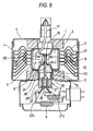
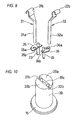
- Magnetron used in a microwave heading apparatus usually comprises, as shown in Fig. 6, a vacuum tube 1 located in the center portion, plural heat radiating fins 2 arranged at the periphery of this vacuum tube 1, a pair of annular magnets 3 arranged coaxially with the vacuum tube 1, a pair of frame yokes 4 for connecting these annular magnets 3 magnetically, and a filter circuit portion 5.
- the vacuum tube 1 includes a cylindrical anode 6, a cathode assembly 7 arranged on an axis of the cylindrical anode 6, plural plate-like vanes 8 arranged in the inner surface of the cylindrical anode 6 radially extending from a center axis of the cylindrical anode 6, plural strap rings 9 and 10 for electrically connecting these vanes on alternate vanes, and a microwave emission antenna 11 of which one end is connected to any one of the plate-like vanes 8.
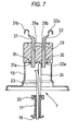
- the cathode assembly 7, as shown in Fig. 7, includes a metal tube 15 which is joined to one opening end edge of the cylindrical anode 6 coaxially with the cylindrical anode 6 and constitutes a part of the vacuum container, a coil-shaped cathode 17 arranged in the axial portion of the cylindrical anode 6, a pair of cathode terminal lead wires 23 and 24 which support the cathode 17 through end-hats 19 and 20 joined to the leading ends of the cathode 17, a stem insulator 29 which is air-tightly joined to an opening end edge of the metal tube 15 and has a pair of through-holes 29a and 29b that pass through the stem insulator 29 in the axial direction of the metal tube 15, a pair of external terminals 31 and 32 of which base end axial portions 31a and 32a are inserted into a pair of through-holes 29a and 29b, and a pair of sealing metal plates 35 and 36 joined to an end surface on the cathode 17 side of the stem insulator 29.
- the cathode 17 is made of thorium/tungsten
- the end-hat 19,20 and the cathode terminal lead wire 23, 24 are made of molybdenum
- the stem insulator 29 is made of ceramic
- the external terminal 31, 32 and the sealing metal plate 35, 36 are made of general conductive metal such as a steel plate.
- Each of the sealing metal plates 35 and 36 includes a terminal fitting hole 35a, 36a into which the leading end of the base end axial portion 31a, 32a of the external terminal 31, 32 which extrudes to the metal tube 15a side from the stem insulator 29 is fitted; and a lead fitting hole 35b, 36b into which a leading end of the cathode terminal lead wire 23, 24 is fitted.
- each of the base end axial portions 31a, 32a and each of the cathode terminal lead wires 23, 24 are fitted respectively into the corresponding terminal fitting hole 35a, 36a or the corresponding lead fitting hole 35b, 36b, they are soldered to the sealing metal plates 35 and 36, so that the electric connection between the corresponding external terminal and cathode terminal lead wire is carried out.
- the sealing metal plates 35 and 36 are soldered onto a metalized layer formed on the end surface of the stem insulator 29, whereby they are fixed onto the end surface of the stem insulator 29 to seal the end surface on the cathode 17 side of the stem insulator 29 air-tightly.
- the reason why the base end axial portions 31a and 32a that are inserted into the stem insulator 29 are provided for the external terminals 31 and 32 is to suppress the length of the expensive molybdenum-made cathode terminal lead wire 23, 24 to a minimum thereby to reduce cost
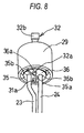
- soldering of the cathode terminal lead wires 23, 24 and the external terminals 31, 32 to the sealing metal plates 35, 36 is performed by the following procedure. Firstly, the cathode terminal lead wires 23, 24, the sealing metal plates 35, 36, the metal tube 15, and the stem insulator 29 are set to a solder reception jig (not shown) that keeps the position of each part shown in Fig. 7. Next, the external terminals 31, 32 are inserted into a pair of through-holes 29a, 29b of the stem insulator 29 and further into the terminal fitting holes 35a, 36a of the sealing metal plates 35, 36. Under this state, soldering is executed. At this time, the state among the cathode terminal lead wires 23, 24, the external terminals 31, 32 and the sealing metal plates 35, 36 is as shown in Fig. 8.
- a pair of bulge portions 39a, 39b are additionally equipped for a top portion of a jig 39 covering the stem insulator 29 in assembly, the leading ends 31b, 32b of the external terminals 31, 32 are fitted into a groove 39c formed by these bulge portions 39a, 39b, and turning of the leading ends 31b, 32b is stopped, whereby the directions of the external terminals 31, 32 can be kept constant.
- a cathode assembly has been proposed in which the leading ends of the external terminals 31, 32 inserted into the stem insulator 29 include radial direction-extensions 31c, 32c which extend in the radial direction of the stem insulator 29, and axial direction-extensions 31d, 32d which extend from the leading ends of these radial direction-extensions 31c, 32c in the axial direction of the stem insulator 29, and in which on the outer side end surface of the stem insulator 29, grooves 29c, 29d for housing and retaining the radial direction-extensions 31c, 32c therein are provided, communicated with each of the through-holes 29a, 29b (for example, refer to Japanese Postexamined Publication 6-73275).
- the stem insulator 29 is usually made of ceramic. After ceramic is press-molded with a predetermined molding die, it is fired to form the stem insulator. Generally, in this method, dimensional accuracy is bad. Therefore, it is necessary for the grooves 29c, 29d to provide a large gap between the external terminals 31, 32 and the grooves 29c, 29d. Accordingly, there is a problem that accuracy of turning stop of the external terminal 31, 32 becomes bad.
- An object of the invention is, in view of the above problems, to provide a magnetron cathode assembly which can realize stopping of turn of an external terminal inserted into a stem insulator without requiring a jig that causes the increase of a manufacturing cost and improvement of the stem insulator, and which can improve soldering performance of the external terminal and simultaneously can reduce the manufacturing cost.
- the magnetron cathode assembly is characterized in that the flat surface of the external terminal that comes into contact with the stop edge of the terminal fitting hole is formed into a slant surface in which the contact strengthens more as fitting into the terminal fitting hole becomes deeper.
- the contact strengthens more as fitting into the terminal fitting hole becomes deeper, which is different from the case in that the flat surface provided for the external terminal is a simple vertical surface in the through-direction of the terminal fitting hole, Therefore, positioning accuracy of fitting improves, and firm fitting in which unstableness is not produced is obtained, so that joint strength by soldering and air-tightly sealing performance can be improved.
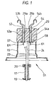
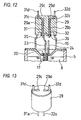
- Fig. 1 shows one embodiment of the magnetron cathode assembly according to the invention.
- a magnetron cathode assembly 51 in this embodiment is used for magnetron used in a microwave heating apparatus such as an electronic oven.
- the magnetron cathode assembly 51 includes a metal tube 15 which is joined to one opening end edge of an anode block coaxially with the anode block and constitutes a part of a vacuum container, a coil-like cathode 17 arranged in the axial portion of the anode block, a pair of cathode terminal lead wires 23 and 24 which support the cathode 17 through end hats 19 and 20 joined to the leading ends of the cathode 17, a stem insulator 29 which is air-tightly joined to an opening end edge of the metal tube 15 and has a pair of through-holes 29a and 29b that pass through the stem insulator 29 in the axial direction of the metal tube 15, a pair of external terminals 53 and 54 of which base end axial portions 53a and 54a are inserted into a pair of through-holes 29a and 29b, and a
- the cathode 17 is made of thorium/tungsten
- the end hat 19,20 and the cathode terminal lead wire 23, 24 are made of molybdenum
- the stem insulator 29 is made of ceramic
- the external terminal 53, 54 and the sealing metal plate 57, 58 are made of general conductive metal such as a steel plate.
- components other than the external terminals 53, 54 and the sealing metal plate 57, 58 are common to the components in the cathode assembly 7 shown in Fig. 7.
- Each of the sealing metal plates 57 and 58 includes a terminal fitting hole 57a, 58a into which a leading end of the base end axial portion 53a, 54a of the external terminal 53, 54 which extrudes to the metal tube 15a side from the stem insulator 29 is fitted; and a lead fitting hole 57b, 58b into which a leading end of the cathode terminal lead wire 23, 24 is fitted.
- the base end axial portions 53a, 54a and the cathode terminal lead wires 23, 24 are fitted respectively into the corresponding terminal fitting holes 57a, 58a or the lead fitting holes 57b, 58b, they are soldered to the sealing metal plates 57 and 58, so that the electric connection between the corresponding external terminal and cathode terminal lead wire is carried out.
- the sealing metal plates 57 and 58 are soldered onto a metallized layer formed on the end surface of the stem insulator 29, whereby they are fixed onto the end surface of the stem insulator 29 to seal the end surface on the cathode 17 side of the stem insulator 29 air-tightly.
- the reason why the base end axial portions 53a and 54a that are inserted into the stem insulator 29 are provided for the external terminals 53 and 54 is to suppress the length of the expensive molybdenum-made cathode terminal lead wire 23, 24 to a minimum thereby to reduce cost
- the base end axial portion 53a, 54a fitted into the terminal fitting hole 57a, 58a is round rod-shaped.
- the leading end of this base end axial portion 53a, 54a has a non-circular section by forming a pair of opposing portions on the peripheral surface into a flat surface 61. It is good for formation of a pair of flat surfaces 61 to utilize press molding that is superior in working performance.
- each of the terminal fitting holes 57a and 58a has a pair of straight stop edges 63 opposed to each other correspondingly to a pair of flat surfaces 61 provided for the leading end of each external terminal 53, 54.
- the terminal fitting hole 57a, 58a shows a rectangular opening shape.
- soldering of the cathode terminal lead wire 23, 24 and the external terminal 53, 54 to the sealing metal plate 57, 58 is performed by the following procedure. Firstly, the cathode terminal lead wires 23, 24, the sealing metal plates 57, 58, the metal tube 15, and the stem insulator 29 are set to a solder reception jig (not shown) that keeps the position of each part shown in Fig. 1. Next, the external terminals 53, 54 are inserted into a pair of through-holes 29a, 29b of the stem insulator 29 and further into the terminal fitting holes 57a, 58a of the sealing metal plates 57, 58. Under this state, soldering is executed. At this time, the state among the cathode terminal lead wires 23, 24, the external terminals 53, 54 and the sealing metal plates 57, 58 is as shown in Fig. 2.
- the flat surface 61 of the external terminal 53, 54 coming into contact with the stop edge 63 of the terminal fitting hole 57a, 58a has a slant surface 65 in which the contact strengthens more as fitting into the terminal fitting hole 57a, 58a becomes deeper.
- the flat surfaces 61 for preventing the turn are formed in two opposing positions.
- the flat surface 61 for preventing the turn is arranged in at least one position, and the number of the flat surfaces 61 for preventing the turn is not limited to that in the above embodiment.
Landscapes
- Microwave Tubes (AREA)
Applications Claiming Priority (2)
| Application Number | Priority Date | Filing Date | Title |
|---|---|---|---|
| JP2003327880A JP2005093330A (ja) | 2003-09-19 | 2003-09-19 | マグネトロン陰極構体 |
| JP2003327880 | 2003-09-19 |
Publications (3)
| Publication Number | Publication Date |
|---|---|
| EP1517351A2 true EP1517351A2 (fr) | 2005-03-23 |
| EP1517351A3 EP1517351A3 (fr) | 2008-02-20 |
| EP1517351B1 EP1517351B1 (fr) | 2009-02-18 |
Family
ID=34191378
Family Applications (1)
| Application Number | Title | Priority Date | Filing Date |
|---|---|---|---|
| EP03030017A Expired - Lifetime EP1517351B1 (fr) | 2003-09-19 | 2003-12-30 | Ensemble cathode pour magnétron |
Country Status (6)
| Country | Link |
|---|---|
| US (1) | US6989634B2 (fr) |
| EP (1) | EP1517351B1 (fr) |
| JP (1) | JP2005093330A (fr) |
| KR (1) | KR20050029096A (fr) |
| CN (1) | CN1599012A (fr) |
| DE (1) | DE60326234D1 (fr) |
Cited By (1)
| Publication number | Priority date | Publication date | Assignee | Title |
|---|---|---|---|---|
| EP3313147A3 (fr) * | 2016-10-24 | 2018-05-02 | LG Electronics Inc. | Magnétron pour four à micro-ondes |
Families Citing this family (11)
| Publication number | Priority date | Publication date | Assignee | Title |
|---|---|---|---|---|
| JP2008108540A (ja) * | 2006-10-25 | 2008-05-08 | Matsushita Electric Ind Co Ltd | マグネトロン |
| CN101840833B (zh) * | 2009-03-16 | 2012-10-17 | 昆山国力真空电器有限公司 | 大功率脉冲磁控管用陶瓷引线 |
| CN102243971A (zh) * | 2010-05-12 | 2011-11-16 | 乐金电子(天津)电器有限公司 | 磁控管的阴极导线结构 |
| CN102820194A (zh) * | 2011-06-07 | 2012-12-12 | 乐金电子(天津)电器有限公司 | 磁控管的阴极陶瓷结构 |
| CN104253008B (zh) * | 2013-06-27 | 2017-05-31 | 乐金电子(天津)电器有限公司 | 微波炉用磁控管的阴极组件及其磁控管 |
| CN104701116A (zh) * | 2013-12-06 | 2015-06-10 | 南京三乐微波技术发展有限公司 | 一种大功率连续波磁控管阴极引出线 |
| DE102015221859A1 (de) * | 2014-11-06 | 2016-05-12 | Hirschmann Car Communication Gmbh | Kontaktierungspin aus Kupferdraht |
| CN109860005B (zh) * | 2018-09-28 | 2021-04-02 | 甘肃虹光电子有限责任公司 | 一种无磁引线接头及其制造方法 |
| CN112331541B (zh) * | 2020-11-13 | 2025-04-01 | 广东格兰仕微波炉电器制造有限公司 | 磁控管阴极组件的投影校准工艺及投影校准工装 |
| CN113284779A (zh) * | 2021-05-11 | 2021-08-20 | 中山市美格电子科技有限公司 | 一种磁控管用陶瓷、引线及引线结构 |
| CN113284778B (zh) * | 2021-05-11 | 2025-07-25 | 中山市美格电子科技有限公司 | 一种高效磁控管 |
Family Cites Families (6)
| Publication number | Priority date | Publication date | Assignee | Title |
|---|---|---|---|---|
| JPH0673275B2 (ja) * | 1985-09-03 | 1994-09-14 | 株式会社東芝 | 電子レンジ用マグネトロン |
| DE3781752T2 (de) * | 1986-09-11 | 1993-01-07 | Tdk Corp | Durchfuehrungstypkondensator, sowie seine verwendung in einem magnetron. |
| EP0339374B1 (fr) * | 1988-04-25 | 1994-03-02 | Matsushita Electronics Corporation | Magnétron |
| KR0161015B1 (ko) * | 1992-07-28 | 1998-12-01 | 강진구 | 마그네트론의 음극지지구조체 |
| JPH0673275A (ja) | 1992-08-28 | 1994-03-15 | Mitsubishi Rayon Co Ltd | ポリエステル樹脂組成物 |
| JP2002352739A (ja) * | 2001-05-30 | 2002-12-06 | Sanyo Electric Co Ltd | マグネトロン |
-
2003
- 2003-09-19 JP JP2003327880A patent/JP2005093330A/ja active Pending
- 2003-12-29 KR KR1020030099111A patent/KR20050029096A/ko not_active Ceased
- 2003-12-30 EP EP03030017A patent/EP1517351B1/fr not_active Expired - Lifetime
- 2003-12-30 US US10/749,288 patent/US6989634B2/en not_active Expired - Lifetime
- 2003-12-30 DE DE60326234T patent/DE60326234D1/de not_active Expired - Lifetime
- 2003-12-31 CN CNA2003101240451A patent/CN1599012A/zh active Pending
Cited By (2)
| Publication number | Priority date | Publication date | Assignee | Title |
|---|---|---|---|---|
| EP3313147A3 (fr) * | 2016-10-24 | 2018-05-02 | LG Electronics Inc. | Magnétron pour four à micro-ondes |
| US10366857B2 (en) | 2016-10-24 | 2019-07-30 | Lg Electronics Inc. | Magnetron for microwave oven |
Also Published As
| Publication number | Publication date |
|---|---|
| CN1599012A (zh) | 2005-03-23 |
| DE60326234D1 (de) | 2009-04-02 |
| EP1517351A3 (fr) | 2008-02-20 |
| JP2005093330A (ja) | 2005-04-07 |
| EP1517351B1 (fr) | 2009-02-18 |
| US20050062427A1 (en) | 2005-03-24 |
| US6989634B2 (en) | 2006-01-24 |
| KR20050029096A (ko) | 2005-03-24 |
Similar Documents
| Publication | Publication Date | Title |
|---|---|---|
| EP1517351B1 (fr) | Ensemble cathode pour magnétron | |
| JPS61156624A (ja) | 電子レンジ用マグネトロン | |
| EP4156418B1 (fr) | Connecteur fixe et ensemble connecteur le comprenant | |
| EP1422737A3 (fr) | Magnétron et procédé de jonction d'élements d'un magnétron | |
| US5508583A (en) | Cathode support structure for magnetron | |
| US4743805A (en) | Anode assembly of magnetron and method of manufacturing the same | |
| EP1810313B1 (fr) | Photomultiplicateur et capteur de rayonnement | |
| US4393681A (en) | Method of manufacturing hermetic sealing member | |
| KR100414192B1 (ko) | 마그네트론 | |
| US4264843A (en) | Magnetron filament assembly | |
| JPH08242041A (ja) | ヒートシンク | |
| KR0133042Y1 (ko) | 마그네트론의 안테나구조 | |
| US3412283A (en) | Coaxial magnetron in which the anode is welded to the body | |
| JPS5918610Y2 (ja) | マグネトロン | |
| KR0125459Y1 (ko) | 마그네트론의 양극부 구조 | |
| KR0122691Y1 (ko) | 마그네트론의 음극지지구조체 | |
| KR930000381B1 (ko) | 마그네트론의 음극구체 | |
| KR200318727Y1 (ko) | 전자렌지용 마그네트론의 애노드 단조장치 | |
| KR0136191Y1 (ko) | 마그네트론의 음극지지구조체 | |
| US3242373A (en) | Electron mounting structure of a high frequency electron tube | |
| JPH0517790Y2 (fr) | ||
| JP3056332U (ja) | セラミック同軸共振体およびそれを用いたフィルター | |
| KR0136192Y1 (ko) | 마그네트론의 음극지지구조체 | |
| US20020145374A1 (en) | Two-piece base for lamp | |
| JPH03250537A (ja) | マグネトロン |
Legal Events
| Date | Code | Title | Description |
|---|---|---|---|
| PUAI | Public reference made under article 153(3) epc to a published international application that has entered the european phase |
Free format text: ORIGINAL CODE: 0009012 |
|
| AK | Designated contracting states |
Kind code of ref document: A2 Designated state(s): AT BE BG CH CY CZ DE DK EE ES FI FR GB GR HU IE IT LI LU MC NL PT RO SE SI SK TR |
|
| AX | Request for extension of the european patent |
Extension state: AL LT LV MK |
|
| PUAL | Search report despatched |
Free format text: ORIGINAL CODE: 0009013 |
|
| AK | Designated contracting states |
Kind code of ref document: A3 Designated state(s): AT BE BG CH CY CZ DE DK EE ES FI FR GB GR HU IE IT LI LU MC NL PT RO SE SI SK TR |
|
| AX | Request for extension of the european patent |
Extension state: AL LT LV MK |
|
| RIC1 | Information provided on ipc code assigned before grant |
Ipc: H01J 23/14 20060101ALI20080116BHEP Ipc: H01J 25/587 20060101ALI20080116BHEP Ipc: H01J 23/05 20060101AFI20050131BHEP |
|
| 17P | Request for examination filed |
Effective date: 20080515 |
|
| GRAP | Despatch of communication of intention to grant a patent |
Free format text: ORIGINAL CODE: EPIDOSNIGR1 |
|
| GRAS | Grant fee paid |
Free format text: ORIGINAL CODE: EPIDOSNIGR3 |
|
| AKX | Designation fees paid |
Designated state(s): DE FR GB |
|
| RAP1 | Party data changed (applicant data changed or rights of an application transferred) |
Owner name: PANASONIC CORPORATION |
|
| GRAA | (expected) grant |
Free format text: ORIGINAL CODE: 0009210 |
|
| AK | Designated contracting states |
Kind code of ref document: B1 Designated state(s): DE FR GB |
|
| REG | Reference to a national code |
Ref country code: GB Ref legal event code: FG4D |
|
| REF | Corresponds to: |
Ref document number: 60326234 Country of ref document: DE Date of ref document: 20090402 Kind code of ref document: P |
|
| PLBE | No opposition filed within time limit |
Free format text: ORIGINAL CODE: 0009261 |
|
| STAA | Information on the status of an ep patent application or granted ep patent |
Free format text: STATUS: NO OPPOSITION FILED WITHIN TIME LIMIT |
|
| 26N | No opposition filed |
Effective date: 20091119 |
|
| PGFP | Annual fee paid to national office [announced via postgrant information from national office to epo] |
Ref country code: GB Payment date: 20141224 Year of fee payment: 12 |
|
| PGFP | Annual fee paid to national office [announced via postgrant information from national office to epo] |
Ref country code: FR Payment date: 20141208 Year of fee payment: 12 |
|
| PGFP | Annual fee paid to national office [announced via postgrant information from national office to epo] |
Ref country code: DE Payment date: 20141223 Year of fee payment: 12 |
|
| REG | Reference to a national code |
Ref country code: DE Ref legal event code: R119 Ref document number: 60326234 Country of ref document: DE |
|
| GBPC | Gb: european patent ceased through non-payment of renewal fee |
Effective date: 20151230 |
|
| REG | Reference to a national code |
Ref country code: FR Ref legal event code: ST Effective date: 20160831 |
|
| PG25 | Lapsed in a contracting state [announced via postgrant information from national office to epo] |
Ref country code: GB Free format text: LAPSE BECAUSE OF NON-PAYMENT OF DUE FEES Effective date: 20151230 Ref country code: DE Free format text: LAPSE BECAUSE OF NON-PAYMENT OF DUE FEES Effective date: 20160701 |
|
| PG25 | Lapsed in a contracting state [announced via postgrant information from national office to epo] |
Ref country code: FR Free format text: LAPSE BECAUSE OF NON-PAYMENT OF DUE FEES Effective date: 20151231 |