EP1513005B1 - Semiconductor device, reflection type liquid crystal display device, and reflection type liquid crystal projector - Google Patents
Semiconductor device, reflection type liquid crystal display device, and reflection type liquid crystal projector Download PDFInfo
- Publication number
- EP1513005B1 EP1513005B1 EP03733360A EP03733360A EP1513005B1 EP 1513005 B1 EP1513005 B1 EP 1513005B1 EP 03733360 A EP03733360 A EP 03733360A EP 03733360 A EP03733360 A EP 03733360A EP 1513005 B1 EP1513005 B1 EP 1513005B1
- Authority
- EP
- European Patent Office
- Prior art keywords
- semiconductor
- liquid crystal
- electrode
- region
- type liquid
- Prior art date
- Legal status (The legal status is an assumption and is not a legal conclusion. Google has not performed a legal analysis and makes no representation as to the accuracy of the status listed.)
- Expired - Lifetime
Links
Images


Classifications
-
- G—PHYSICS
- G02—OPTICS
- G02F—OPTICAL DEVICES OR ARRANGEMENTS FOR THE CONTROL OF LIGHT BY MODIFICATION OF THE OPTICAL PROPERTIES OF THE MEDIA OF THE ELEMENTS INVOLVED THEREIN; NON-LINEAR OPTICS; FREQUENCY-CHANGING OF LIGHT; OPTICAL LOGIC ELEMENTS; OPTICAL ANALOGUE/DIGITAL CONVERTERS
- G02F1/00—Devices or arrangements for the control of the intensity, colour, phase, polarisation or direction of light arriving from an independent light source, e.g. switching, gating or modulating; Non-linear optics
- G02F1/01—Devices or arrangements for the control of the intensity, colour, phase, polarisation or direction of light arriving from an independent light source, e.g. switching, gating or modulating; Non-linear optics for the control of the intensity, phase, polarisation or colour
- G02F1/13—Devices or arrangements for the control of the intensity, colour, phase, polarisation or direction of light arriving from an independent light source, e.g. switching, gating or modulating; Non-linear optics for the control of the intensity, phase, polarisation or colour based on liquid crystals, e.g. single liquid crystal display cells
- G02F1/133—Constructional arrangements; Operation of liquid crystal cells; Circuit arrangements
- G02F1/136—Liquid crystal cells structurally associated with a semi-conducting layer or substrate, e.g. cells forming part of an integrated circuit
- G02F1/1362—Active matrix addressed cells
- G02F1/1368—Active matrix addressed cells in which the switching element is a three-electrode device
-
- G—PHYSICS
- G02—OPTICS
- G02F—OPTICAL DEVICES OR ARRANGEMENTS FOR THE CONTROL OF LIGHT BY MODIFICATION OF THE OPTICAL PROPERTIES OF THE MEDIA OF THE ELEMENTS INVOLVED THEREIN; NON-LINEAR OPTICS; FREQUENCY-CHANGING OF LIGHT; OPTICAL LOGIC ELEMENTS; OPTICAL ANALOGUE/DIGITAL CONVERTERS
- G02F1/00—Devices or arrangements for the control of the intensity, colour, phase, polarisation or direction of light arriving from an independent light source, e.g. switching, gating or modulating; Non-linear optics
- G02F1/01—Devices or arrangements for the control of the intensity, colour, phase, polarisation or direction of light arriving from an independent light source, e.g. switching, gating or modulating; Non-linear optics for the control of the intensity, phase, polarisation or colour
- G02F1/13—Devices or arrangements for the control of the intensity, colour, phase, polarisation or direction of light arriving from an independent light source, e.g. switching, gating or modulating; Non-linear optics for the control of the intensity, phase, polarisation or colour based on liquid crystals, e.g. single liquid crystal display cells
- G02F1/133—Constructional arrangements; Operation of liquid crystal cells; Circuit arrangements
- G02F1/136—Liquid crystal cells structurally associated with a semi-conducting layer or substrate, e.g. cells forming part of an integrated circuit
-
- G—PHYSICS
- G02—OPTICS
- G02F—OPTICAL DEVICES OR ARRANGEMENTS FOR THE CONTROL OF LIGHT BY MODIFICATION OF THE OPTICAL PROPERTIES OF THE MEDIA OF THE ELEMENTS INVOLVED THEREIN; NON-LINEAR OPTICS; FREQUENCY-CHANGING OF LIGHT; OPTICAL LOGIC ELEMENTS; OPTICAL ANALOGUE/DIGITAL CONVERTERS
- G02F1/00—Devices or arrangements for the control of the intensity, colour, phase, polarisation or direction of light arriving from an independent light source, e.g. switching, gating or modulating; Non-linear optics
- G02F1/01—Devices or arrangements for the control of the intensity, colour, phase, polarisation or direction of light arriving from an independent light source, e.g. switching, gating or modulating; Non-linear optics for the control of the intensity, phase, polarisation or colour
- G02F1/13—Devices or arrangements for the control of the intensity, colour, phase, polarisation or direction of light arriving from an independent light source, e.g. switching, gating or modulating; Non-linear optics for the control of the intensity, phase, polarisation or colour based on liquid crystals, e.g. single liquid crystal display cells
- G02F1/133—Constructional arrangements; Operation of liquid crystal cells; Circuit arrangements
- G02F1/1333—Constructional arrangements; Manufacturing methods
- G02F1/1335—Structural association of cells with optical devices, e.g. polarisers or reflectors
-
- G—PHYSICS
- G02—OPTICS
- G02F—OPTICAL DEVICES OR ARRANGEMENTS FOR THE CONTROL OF LIGHT BY MODIFICATION OF THE OPTICAL PROPERTIES OF THE MEDIA OF THE ELEMENTS INVOLVED THEREIN; NON-LINEAR OPTICS; FREQUENCY-CHANGING OF LIGHT; OPTICAL LOGIC ELEMENTS; OPTICAL ANALOGUE/DIGITAL CONVERTERS
- G02F1/00—Devices or arrangements for the control of the intensity, colour, phase, polarisation or direction of light arriving from an independent light source, e.g. switching, gating or modulating; Non-linear optics
- G02F1/01—Devices or arrangements for the control of the intensity, colour, phase, polarisation or direction of light arriving from an independent light source, e.g. switching, gating or modulating; Non-linear optics for the control of the intensity, phase, polarisation or colour
- G02F1/13—Devices or arrangements for the control of the intensity, colour, phase, polarisation or direction of light arriving from an independent light source, e.g. switching, gating or modulating; Non-linear optics for the control of the intensity, phase, polarisation or colour based on liquid crystals, e.g. single liquid crystal display cells
- G02F1/133—Constructional arrangements; Operation of liquid crystal cells; Circuit arrangements
- G02F1/1333—Constructional arrangements; Manufacturing methods
- G02F1/1343—Electrodes
-
- G—PHYSICS
- G02—OPTICS
- G02F—OPTICAL DEVICES OR ARRANGEMENTS FOR THE CONTROL OF LIGHT BY MODIFICATION OF THE OPTICAL PROPERTIES OF THE MEDIA OF THE ELEMENTS INVOLVED THEREIN; NON-LINEAR OPTICS; FREQUENCY-CHANGING OF LIGHT; OPTICAL LOGIC ELEMENTS; OPTICAL ANALOGUE/DIGITAL CONVERTERS
- G02F1/00—Devices or arrangements for the control of the intensity, colour, phase, polarisation or direction of light arriving from an independent light source, e.g. switching, gating or modulating; Non-linear optics
- G02F1/01—Devices or arrangements for the control of the intensity, colour, phase, polarisation or direction of light arriving from an independent light source, e.g. switching, gating or modulating; Non-linear optics for the control of the intensity, phase, polarisation or colour
- G02F1/13—Devices or arrangements for the control of the intensity, colour, phase, polarisation or direction of light arriving from an independent light source, e.g. switching, gating or modulating; Non-linear optics for the control of the intensity, phase, polarisation or colour based on liquid crystals, e.g. single liquid crystal display cells
- G02F1/133—Constructional arrangements; Operation of liquid crystal cells; Circuit arrangements
- G02F1/136—Liquid crystal cells structurally associated with a semi-conducting layer or substrate, e.g. cells forming part of an integrated circuit
- G02F1/1362—Active matrix addressed cells
- G02F1/136277—Active matrix addressed cells formed on a semiconductor substrate, e.g. of silicon
-
- G—PHYSICS
- G02—OPTICS
- G02F—OPTICAL DEVICES OR ARRANGEMENTS FOR THE CONTROL OF LIGHT BY MODIFICATION OF THE OPTICAL PROPERTIES OF THE MEDIA OF THE ELEMENTS INVOLVED THEREIN; NON-LINEAR OPTICS; FREQUENCY-CHANGING OF LIGHT; OPTICAL LOGIC ELEMENTS; OPTICAL ANALOGUE/DIGITAL CONVERTERS
- G02F1/00—Devices or arrangements for the control of the intensity, colour, phase, polarisation or direction of light arriving from an independent light source, e.g. switching, gating or modulating; Non-linear optics
- G02F1/01—Devices or arrangements for the control of the intensity, colour, phase, polarisation or direction of light arriving from an independent light source, e.g. switching, gating or modulating; Non-linear optics for the control of the intensity, phase, polarisation or colour
- G02F1/13—Devices or arrangements for the control of the intensity, colour, phase, polarisation or direction of light arriving from an independent light source, e.g. switching, gating or modulating; Non-linear optics for the control of the intensity, phase, polarisation or colour based on liquid crystals, e.g. single liquid crystal display cells
- G02F1/133—Constructional arrangements; Operation of liquid crystal cells; Circuit arrangements
- G02F1/136—Liquid crystal cells structurally associated with a semi-conducting layer or substrate, e.g. cells forming part of an integrated circuit
- G02F1/1362—Active matrix addressed cells
- G02F1/136213—Storage capacitors associated with the pixel electrode
-
- G—PHYSICS
- G02—OPTICS
- G02F—OPTICAL DEVICES OR ARRANGEMENTS FOR THE CONTROL OF LIGHT BY MODIFICATION OF THE OPTICAL PROPERTIES OF THE MEDIA OF THE ELEMENTS INVOLVED THEREIN; NON-LINEAR OPTICS; FREQUENCY-CHANGING OF LIGHT; OPTICAL LOGIC ELEMENTS; OPTICAL ANALOGUE/DIGITAL CONVERTERS
- G02F2203/00—Function characteristic
- G02F2203/02—Function characteristic reflective
-
- H—ELECTRICITY
- H10—SEMICONDUCTOR DEVICES; ELECTRIC SOLID-STATE DEVICES NOT OTHERWISE PROVIDED FOR
- H10D—INORGANIC ELECTRIC SEMICONDUCTOR DEVICES
- H10D86/00—Integrated devices formed in or on insulating or conducting substrates, e.g. formed in silicon-on-insulator [SOI] substrates or on stainless steel or glass substrates
- H10D86/40—Integrated devices formed in or on insulating or conducting substrates, e.g. formed in silicon-on-insulator [SOI] substrates or on stainless steel or glass substrates characterised by multiple TFTs
- H10D86/60—Integrated devices formed in or on insulating or conducting substrates, e.g. formed in silicon-on-insulator [SOI] substrates or on stainless steel or glass substrates characterised by multiple TFTs wherein the TFTs are in active matrices
-
- H—ELECTRICITY
- H10—SEMICONDUCTOR DEVICES; ELECTRIC SOLID-STATE DEVICES NOT OTHERWISE PROVIDED FOR
- H10D—INORGANIC ELECTRIC SEMICONDUCTOR DEVICES
- H10D86/00—Integrated devices formed in or on insulating or conducting substrates, e.g. formed in silicon-on-insulator [SOI] substrates or on stainless steel or glass substrates
- H10D86/80—Integrated devices formed in or on insulating or conducting substrates, e.g. formed in silicon-on-insulator [SOI] substrates or on stainless steel or glass substrates characterised by multiple passive components, e.g. resistors, capacitors or inductors
Definitions
- the present invention relates to a semiconductor device for constituting an active matrix drive portion in a reflection type liquid crystal display apparatus for active matrix display, a reflection type liquid crystal display apparatus for active matrix display, and a reflection type liquid crystal projector using a reflection type liquid crystal display apparatus for active matrix display.
- the reflection type liquid crystal display apparatus 9 is comprised, as a whole, of a liquid crystal layer 33 formed by injecting a liquid crystal between a semiconductor device portion 50 constituting an active matrix drive portion and a counter transparent substrate 32 provided with a counter transparent electrode 31 functioning in common for each pixel.
- the semiconductor device portion 50 comprises a semiconductor substrate (semiconductor base) 11 such as a silicon substrate of a first conduction type, for example, P type, on which switching transistors 13 and signal accumulation capacitors 55 are provided on the basis of each unit region for constituting a pixel Px.
- the switching transistor 13 is configured as a MIS (Metal Insulator Semiconductor) type or MOS (Metal Oxide Semiconductor) type transistor in which a source region 13S and a drain region 13D of a second conduction type (namely, of N type where the semiconductor substrate 11 is of P type) are formed in the semiconductor substrate 11, and a gate electrode 13G formed of polysilicon or the like is formed on the region between the source region 13S and the drain region 13D, with a thin insulating layer 12a therebetween which constitutes a part of an insulating layer 12 formed of silicon dioxide or the like.
- MIS Metal Insulator Semiconductor
- MOS Metal Oxide Semiconductor
- the signal accumulation capacitor 55 is configured as a MIS type or MOS type transistor in which semiconductor regions 55D and 55S of the same second conduction type as that of the source region 13S and the drain region 13D of the switching transistor 13 (namely, of N type where the semiconductor substrate 11 is of P type) are formed in the semiconductor substrate 11, and an electrode 55G is formed on the region between the semiconductor regions 55D and 55S, with a thin insulating layer 12b therebetween which constitutes a part of the insulating layer 12. With an appropriate potential impressed on the semiconductor regions 55D and 55S, a channel 55c is formed at a portion beneath the electrode 55G between the semiconductor regions 55D and 55S, and a capacitance is formed.
- high-concentration bias semiconductor regions 57 of the same first conduction type as that of the semiconductor substrate 11 (namely, of P type where the semiconductor substrate 11 is of P type), for impressing a bias potential such as earth potential on the semiconductor substrate 11, are formed in the semiconductor substrate 11 on the basis of each unit region constituting a pixel Px.
- a scan line (scan electrode) 21 is formed in connection with the gate electrode 13G of the switching transistor 13
- a signal line (signal electrode) 23 is formed in connection with the source region 13S of the switching transistor 13
- a wiring 25 is formed for interconnection between the drain region 13D of the switching transistor 13 and the electrode 55G of the signal accumulation capacitor 55
- a bias electrode 59 is formed in connection with the semiconductor regions 55D and 55S of the signal accumulation capacitor 55 and with the bias semiconductor region 57.
- a reflection electrode 19 for constituting a pixel electrode is formed in connection with the wiring 25, i.e., in connection with the drain region 13D of the switching transistor 13 and the electrode 55G of the signal accumulation capacitor 55.
- the reflection type liquid crystal display apparatus 9 has a structure in which a multiplicity of the scan lines 21 are arranged in a vertical direction of a display screen, a multiplicity of the signal lines 23 are arranged in a horizontal direction of the display screen, and each of the portions at intersections of the scan lines 21 and the signal lines 23 is constituted as the pixel Px as above-mentioned.
- the scan lines 21 are sequentially selected by a scan line drive circuit, and a predetermined potential is impressed on the gate electrode 13G of the switching transistor 13 for the pixel connected to the scan line 21 thus selected, whereby the switching transistor 13 for the pixel under consideration is turned ON, and a signal voltage is impressed on the source region 13S of the switching transistor 13 for the pixel in consideration through the signal line 23 by a signal line drive circuit, whereby a signal charge is accumulated in the capacitance of the signal accumulation capacitor 55 for the pixel under consideration through the drain region 13D of the switching transistor 13 for the pixel under consideration.
- the signal charge thus accumulated is impressed on the reflection electrode 19 for the pixel under consideration, an electric field according to the signal voltage is impressed between the counter transparent electrode 31 functioning in common for each pixel and the reflection electrode 19 for the pixel under consideration, and, according to this, the rotatory polarization of light at the portion of the pixel under consideration is controlled by the liquid crystal layer 33.
- the semiconductor regions 55D and 55S constituting the signal accumulation capacitor 55 are of a conduction type different from that of the semiconductor substrate (semiconductor base) 11, i.e., they are of the same conduction type as that of the source region 13S and the drain region 13D of the switching transistor 13. Therefore, for separation between the switching transistor region and the signal accumulation capacitor region, the distance between the switching transistor region and the signal accumulation capacitor region, i.e., the distance d between the drain region 13D of the switching transistor 13 and the semiconductor region 55D of the signal accumulation capacitor 55 must be large at least to a certain extent. As a result, the area of the pixel Px is large, and the number of pixels which can be formed in a predetermined size is small.
- the semiconductor regions 55D and 55S constituting the signal accumulation capacitor 55 are of a conduction type different from that of the semiconductor substrate (semiconductor base) 11, the bias semiconductor region 57 of the same conduction type as that of the semiconductor substrate 11, for impressing a bias potential such as an earth potential on the semiconductor substrate 11, must be formed in the semiconductor substrate 11; accordingly, the area of the pixel Px is enlarged and the number of pixels which can be formed in a predetermined size is reduced.
- the present invention aims at realizing a reduction in the area of a pixel without degrading noise resistance.
- JP 055 164 875 A discloses another type of semiconductor device. According to said document, where is provided a P-type semiconductor substrate having a P-type capacitance region 13 and an N-type drain region and source region 11. 12 forming a transistor. The capacitor is connected to a power (voltage) source line 15. However, that document does not disclose a connection of the capacitor to a bias electrode.
- JP 10 039332 A Another type of semiconductor device is shown and described in JP 10 039332 A .
- conductive layers which constitute holding capacitors are formed by each of respective pixels below pixel electrodes which are reflection electrodes.
- Semiconductor regions or other conductive layers which constitute the other terminals of the holding capacitors are formed via insulating films below or above the conductive layers.
- the conductive layers are electrically connected to transistors for driving the pixel electrodes.
- the semiconductor regions are electrically connected to wiring layers which are connected to a LC common voltage applied from an opposite substrate.
- Still another Semiconductor device is disclosed in US-A-6 133 976 .
- picture element electrodes of a spatial light modulation device are located in the form of a two-dimensional matrix, an opposite electrode being located at a spacing from the picture element electrodes, and a light modulation layer being located between the opposite electrode and the picture element electrodes.
- An insulation film is formed between the light modulation layer and the picture element electrodes.
- An electrically conductive film is formed with the insulation film intervening between the electrically conductive film and the picture element electrodes, and covers at least a portion of a gap between adjacent picture element electrodes.
- the active-matrix substrate described in US-A-6 133 976 differs from that defined in appended claim 1 at least in that its signal accumulation capacitor has only one semiconductor region provided in the semiconductor base and that said one semiconductor region of the signal accummulation capacitor is not connected to a bias electrode.
- JP 61 119072 A shows a semiconductor capacity device which teaches to prevent the generation of a parasitic capacity between an n + diffusion part and a substrate by separating the n + diffusion part from the substrate by arranging it in an n type well.
- JP 10 293323 discloses a liquid crystal panel with a transistor being comprised of a source zone and a drain zone made of a high impurity introduction layer formed on a substrate surface at both sides of a gate electrode. Moreover, there is also formed a storage capacitor. There is a disadvantage of the state of the art that the contact regions for the substate are sensitive for noise carried on the substrate.
- the semiconductor regions for constituting the signal accumulation capacitor are of the same conduction type as that of the semiconductor base, i.e., of a conduction type different from that of the source region and the drain region of the switching transistor. Therefore, for separation between the switching transistor region and the signal accumulation capacitor region, the distance between the switching transistor region and the signal accumulation capacitor region, i.e., the distance between the drain region of the switching transistor and the semiconductor region on the switching transistor side of the signal accumulation capacitor can be made to be sufficiently small, whereby the area of the pixel can be reduced, and the number of pixels which can be formed in a predetermined size can be enlarged.
- the reduction in the area of the pixel can be realized in the same manner as above also by forming a bias semiconductor region of the first conduction type on the semiconductor base, separately from the semiconductor regions for constituting the signal accumulation capacitor, as defined in appended dependent claim 2. Since the semiconductor region for constituting the signal accumulation capacitor is of the same conduction type as that of the semiconductor base, the semiconductor regions for constituting the signal accumulation capacitor are made to serve also as bias semiconductor regions of the semiconductor base, and therefore, the area of the pixel can be further reduced, and the number of pixels which can be formed in a predetermined size can be further enlarged.
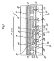
- Fig. 1 illustrates a first embodiment of the reflection type liquid crystal display apparatus according to the present invention which comprises as a semiconductor device portion a first embodiment of the semiconductor device according to the present invention.
- the reflection type liquid crystal display apparatus 1 has, as a whole, a configuration in which a liquid crystal layer 33 is formed by injecting a liquid crystal between a semiconductor device portion 10 for constituting an active matrix drive portion and a counter transparent substrate 32 provided with a counter transparent electrode 31 functioning in common for each pixel.
- the semiconductor device portion 10 has a configuration in which a switching transistor 13 and a signal accumulation capacitor 15 are formed on a semiconductor substrate (semiconductor base) 11 such as a silicon substrate of a first conduction type, for example, P type, on the basis of each unit region for constituting a pixel Px.
- a semiconductor substrate semiconductor base
- semiconductor substrate 11 semiconductor substrate of a first conduction type, for example, P type
- the switching transistor 13 is constituted as a MIS type or MOS type transistor in which a source region 13S and a drain region 13D of a second conduction type (namely, of N type where the semiconductor substrate 11 is of P type) are formed in the semiconductor substrate 11, and a gate electrode 13G formed of polysilicon or the like is formed on the region between the source region 13S and the drain region 13D, with a thin insulating layer 12a therebetween which constitutes a part of an insulating layer 12 formed of silicon dioxide or the like.
- a source region 13S and a drain region 13D of a second conduction type namely, of N type where the semiconductor substrate 11 is of P type
- the signal accumulation capacitor 15 is constituted as a MIS type or MOS type transistor in which high-concentration semiconductor regions 15D and 15S of the same first conduction type as that of the semiconductor substrate 11 (namely, of P type where the semiconductor substrate 11 is of P type) are formed in the semiconductor substrate 11, and an electrode 15G is formed on the region between the semiconductor regions 15D and 15S, with a thin insulating layer 12b therebetween which constitutes a part of the insulating layer 12. With an appropriate potential impressed on the semiconductor regions 15D and 15S, a channel 15c is formed at a portion beneath the electrode 15G between the semiconductor regions 15D and 15S, and a capacitance is formed.
- a high-concentration bias semiconductor region 17 of the same first conduction type as that of the semiconductor substrate 11 (namely, of P type where the semiconductor substrate 11 is of P type), for impressing a bias potential such as an earth potential on the semiconductor substrate 11, is formed in the semiconductor substrate 11 on the basis of each unit region for constituting the pixel Px.
- a scan line (scan electrode) 21 is formed in connection with the gate electrode 13G of the switching transistor 13
- a signal line (signal electrode) 23 is formed in connection with the source region 13S of the switching transistor 13
- a wiring 25 is formed for interconnection between the drain region 13D of the switching transistor 13 and the electrode 15G of the signal accumulation capacitor 15, and a bias electrode 27 is formed in connection with the semiconductor regions 15D and 15S of the signal accumulation capacitor 15 and the bias semiconductor region 17.
- a reflection electrode 19 for constituting a pixel electrode is formed in connection with the wiring 25, i.e., in connection with the drain region 13D of the switching transistor 13 and the electrode 15G of the signal accumulation capacitor 15.
- the reflection type liquid crystal display apparatus 1 has a configuration in which a multiplicity of scan lines 21 are arranged in a vertical direction of a display screen, a multiplicity of signal lines 23 are arranged in a horizontal direction of the display screen, and the portion of each of the intersections of the scan lines 21 and the signal lines 23 is constituted as a pixel Px as above-described.
- a drive circuit is so constituted that with the bias electrodes 27 earthed, with the earth potential impressed on the semiconductor regions 15D and 15S of the signal accumulation capacitors 15 and the bias semiconductor regions 17, and with a predetermined potential impressed on the counter transparent electrode 31 functioning in common for each pixel, the scan lines 21 are sequentially selected by a scan line drive circuit, and a predetermined potential is impressed on the gate electrode 13G of the switching transistor 13 for the pixel connected to the scan line 21 thus selected, whereby the switching transistor 13 for the pixel under consideration is turned ON, and a signal voltage is impressed on the source region 13S of the switching transistor 13 for the pixel under consideration through the signal line 23 by a signal line drive circuit, whereby a signal charge is accumulated in the capacitance of the signal accumulation capacitor 15 for the pixel under consideration through the drain region 13D of the switching transistor 13 for the pixel under consideration.
- the signal charge thus accumulated is impressed on the reflection electrode 19 for the pixel under consideration, and an electric field according to the signal voltage is impressed between the counter transparent electrode 31 functioning in common for each pixel and the reflection electrode 19 for the pixel under consideration.
- the rotatory polarization state of the liquid crystal at the portion of the pixel under consideration having a liquid crystal capacity Cx of the liquid crystal layer 33 is controlled, and the light which is incident on the reflection type liquid crystal display apparatus 1 from the outside of the counter transparent substrate 32, is transmitted through the portion of the pixel under consideration of the liquid crystal layer 33, is reflected by the reflection electrode 19, is again transmitted through the portion of the pixel under consideration of the liquid crystal layer 33 and goes out to the outside of the counter transparent substrate 32 is modulated, and the light in a predetermined polarization direction is outputted, whereby an image is displayed on the reflection type liquid crystal display apparatus 1.
- the semiconductor regions 15D and 15S for constituting the signal accumulation capacitor 15 are of the same conduction type as that of the semiconductor substrate (semiconductor base) 11, i.e., of the conduction type different from that of the source region 13S and the drain region 13D of the switching transistor 13. Therefore, for separation between the switching transistor region and the signal accumulation capacitor region, the distance between the switching transistor region and the signal accumulation capacitor region, i.e., the distance d between the drain region 13D of the switching transistor 13 and the semiconductor region 15D. of the signal accumulation capacitor 15 can be made to be sufficiently small, whereby the area of the pixel Px can be reduced, and the number of pixels which can be formed in a predetermined size can be enlarged.
- the bias semiconductor region 17 not only the bias semiconductor region 17 but also the semiconductor regions 15D and 15S for constituting the signal accumulation capacitors 15 are used as the regions for impressing the bias potential on the semiconductor substrate 11; accordingly, the bias potential is stably impressed on the semiconductor substrate 11, and noise resistance is enhanced.
- a bias potential different from the earth potential may be impressed on the semiconductor regions 15D and 15S of the signal accumulation capacitor 15 and the bias semiconductor region 17.
- the semiconductor substrate (semiconductor base) 11, the semiconductor regions 15D and 15S of the signal accumulation capacitor 15 and the bias semiconductor region 17 may be of N type, while the source region 13S and the drain region 13D of the switching transistor 13 may be of P type.
- a configuration may be adopted in which, for example, a semiconductor base of P type is formed on a semiconductor substrate of N type, and a source region and a drain region of N type for constituting the switching transistor, a semiconductor region of P type for constituting the signal accumulation capacitor, and a bias semiconductor region of P type are formed in the semiconductor base of the P type.
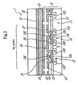
- Fig. 2 illustrates a second embodiment of the reflection type liquid crystal display apparatus according to the present invention which comprises as a semiconductor device portion a second embodiment of the semiconductor device according to the present invention.
- a bias semiconductor region is not formed in the semiconductor substrate 11 separately from the high-concentration semiconductor regions 15D and 15S of the same conduction type as that of the semiconductor substrate 11 for constituting the signal accumulation capacitor 15, and, instead, the semiconductor regions 15D and 15S for constituting the signal accumulation capacitor 15 are made to serve also as the bias semiconductor region for impressing the bias potential on the semiconductor substrate 11.
- a bias electrode 27 is formed on the insulating layer 14 in the state of being connected to the semiconductor regions 15D and 15S, and the bias electrode 27 is connected to a bias potential point such as an earth potential point, whereby a bias potential such as the earth potential is impressed on the semiconductor regions 15D and 15S.
- a bias potential point such as an earth potential point
- the distance between the switching transistor region and the signal accumulation capacitor region i.e., the distance between the drain region 13D of the switching transistor 13 and the semiconductor region 15D of the signal accumulation capacitor 15 can be made to be sufficiently small.
- the portion for forming the bias semiconductor region 17 in the embodiment shown in Fig. 1 can be cut from the pixel region. Therefore, as compared with the embodiment shown in Fig. 1 , the area of the pixel Px can be further reduced, and the number of pixels which can be formed in a predetermined size can be further enlarged.
- the area of the pixel Px can be made to be sufficiently small, even without reducing the area of the semiconductor regions 15D and 15S of the signal accumulation capacitor 15 serving also as the bias semiconductor region. As a result, the bias potential is stably impressed on the semiconductor substrate 11, and noise resistance is enhanced.
- the semiconductor substrate (semiconductor base) 11 and the semiconductor regions 15D and 15S of the signal accumulation capacitor 15 may be of N type, while the source region 13S and the drain region 13D of the switching transistor 13 may be of P type.
- a configuration may be adopted in which, for example, a semiconductor base of P type is formed on a semiconductor substrate of N type, and a source region and a drain region of N type for constituting the switching transistor and semiconductor regions of P type for constituting the signal accumulation capacitor are formed in the semiconductor base of the P type.
- Fig. 3 illustrates a reflection type liquid crystal display apparatus not according to the present invention which comprises as a semiconductor device portion a semiconductor device not according to the present invention.
- the switching transistor 13 is configured in the same manner as those in the embodiments shown in Figs. 1 and 2 .
- the signal accumulation capacitor 15 has a configuration in which an electrode 15G is formed on a region, adjacent to the drain region 13D of the switching transistor 13, of the semiconductor substrate (semiconductor base) 11, with a thin insulating layer 12b therebetween which constitutes a part of the insulating layer 12. With an appropriate potential impressed on the electrode 15G, a channel 15c is formed at a portion beneath the electrode 15G adjacent to the drain region 13D, and a capacitance is formed.
- a high-concentration bias semiconductor region 17 of the same first conduction type as that of the semiconductor substrate 11 (namely, of P type where the semiconductor substrate 11 is of P type), for impressing a bias potential such as the earth potential on the semiconductor substrate 11, is formed in the semiconductor substrate 11 on the basis of each unit region for constituting a pixel Px.
- a scan line 21 is formed in connection with the gate electrode 13G of the switching transistor 13
- a signal line 23 is formed in connection with the source region 13S of the switching transistor 13
- a bias electrode 27 is formed in connection with the electrode 15G of the signal accumulation capacitor 15 and the bias semiconductor region 17.
- a reflection electrode 19 for constituting a pixel electrode is formed in connection with the drain region 13D of the switching transistor 13.
- a drive circuit is so constituted that, as shown in Fig. 5 , with the bias electrode 27 earthed, with the earth potential impressed on the electrode 15G of the signal accumulation capacitor 15 and the bias semiconductor region 17, and with a predetermined potential impressed on the counter transparent electrode 31 functioning in common for each pixel, the scan lines 21 are sequentially selected by a scan line drive circuit, and a predetermined potential is impressed on the gate electrode 13G of the switching transistor 13 for the pixel connected to the scan line 21 thus selected, whereby the switching transistor 13 for the pixel under consideration is turned ON, and a signal voltage is impressed on the source region 13S of the switching transistor 13 for the pixel under consideration through a signal line 23 by a signal line drive circuit, whereby a signal charge is accumulated in the capacitance of the signal accumulation capacitor 15 for the pixel under consideration through the drain region 13D of the switching transistor 13 for the pixel under consideration.
- the signal charge thus accumulated is impressed on the reflection electrode 19 for the pixel under consideration, whereby an image is displayed on the reflection type liquid crystal display apparatus 1, in the same manner as in the embodiments shown in Figs. 1 and 2 .
- a semiconductor region for constituting the signal accumulation capacitor 15 is not formed in the semiconductor substrate 11 separately from the drain region 13D of the switching transistor 13. Therefore, even though the bias semiconductor region 17 is formed on the semiconductor substrate 11, the area of the pixel Px can be reduced, and the number of pixels which can be formed in a predetermined size can be enlarged.
- a bias potential different from the earth potential may be impressed on the electrode 15G of the signal accumulation capacitor 15 and the bias semiconductor region 17.
- bias potentials different from each other may be impressed respectively on the electrode 15G and the bias semiconductor region 17.
- the semiconductor substrate (semiconductor base) 11 and the bias semiconductor region 17 may be of N type, while the source region 13S and the drain region 13D of the switching transistor 13 may be of P type.
- a configuration may be adopted in which, for example, a semiconductor base of P type is formed on a semiconductor substrate of N type, and a source region and a drain region of N type for constituting the switching transistor and a bias semiconductor region of P type are formed in the semiconductor base of the P type.
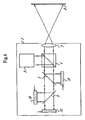
- the reflection type liquid crystal display apparatus according to the present invention constituted as those in the above-described embodiments, can be used, for example, for a reflection type liquid crystal projector (projection type display apparatus).
- Fig. 6 illustrates an embodiment of the reflection type liquid crystal projector according to the present invention, using the reflection type liquid crystal display apparatus according to the present invention.
- non-polarized white light as parallel rays having a uniform intensity distribution in a predetermined region on a plane orthogonal to the center of light beam is emitted from an illumination unit 3 comprising a white light source therein.
- the light beam thus emitted is incident on a polarized light beam splitter 4, where it is split into a light beam of S polarized light reflected by the polarized light beam splitter 4, and a light beam of P polarized light transmitted through the polarized light beam splitter 4.
- the light beam of S polarized light reflected by the polarized light beam splitter 4 is incident on a red reflector 5, where red light in the light beam of S polarized light is reflected by the red reflector 5, whereas green light and blue light are transmitted through the red reflector 5.
- the green light and blue light transmitted through the red reflector 5 are incident on a blue reflector 6, where the blue light is reflected by the blue reflector 6, whereas the green light is transmitted through the blue reflector 6.
- the red light reflected by the red reflector 5 is incident on a reflection type liquid crystal display apparatus 1R for red
- the green light transmitted through the blue reflector 6 is incident on a reflection type liquid crystal display apparatus 1G for green
- the blue light reflected by the blue reflector 6 is incident on a reflection type liquid crystal display apparatus 1B for blue.
- the reflection type liquid crystal display apparatuses 1R, 1G, and 1B are each a reflection type liquid crystal display apparatus according to the present invention, which is constituted as in the embodiment shown in Fig. 1 , Fig. 2 or in the example useful for understanding the invention shown in Fig. 3 , and in which image data are written by red, green, and blue picture signals (color signals), respectively.
- the red light incident on the reflection type liquid crystal display apparatus 1R, the green light incident on the reflection type liquid crystal display apparatus 1G, and the blue light incident on the reflection type liquid crystal display apparatus 1B are modulated respectively by the reflection type liquid crystal display apparatuses 1R, 1G, and 1B based on the picture signals, are then reflected, and again combined with each other by the red reflector 5 and the blue reflector 6.
- the P polarized light component is transmitted through the polarized light beam splitter 4 as image light, which is enlargedly projected on a screen 8 by a projection lens 7.
- the area of each pixel in the reflection type liquid crystal display apparatuses 1R, 1G, and 1B can be reduced, and the number of pixels which can be formed in a predetermined size can be enlarged, as described above. Therefore, where the reflection type liquid crystal display apparatuses 1R, 1G, and 1B are manufactured in a predetermined size, the number of the pixels in the reflection type liquid crystal display apparatuses 1R, 1G, and 1B can be enlarged, and a high-resolution image can be projected on the screen 8.
- the size of the reflection type liquid crystal display apparatuses 1R, 1G, and 1B can be reduced, and, hence, the size of the reflection type liquid crystal projector 2 can be reduced.
- the reflection type liquid crystal projector according to the present invention is not limited to the one shown in the figure. It suffices for the reflection type liquid crystal projector to comprise an illumination optical system for emitting the light from a white light source in the form of a light beam having a uniform intensity distribution in a predetermined region on a plane orthogonal to the center of the light beam, a decomposing optical system for splitting the thus emitted light beam into a plurality of color light beams such as red, green and blue light beams, reflection type liquid crystal display apparatuses according to the present invention on which the thus split color light beams are respectively incident, a combining optical system for combining color image light beams emitted from the reflection type liquid crystal display apparatuses for the colors, and a projection optical system for projecting the combined image light on a screen.
- an illumination optical system for emitting the light from a white light source in the form of a light beam having a uniform intensity distribution in a predetermined region on a plane orthogonal to the center of the light beam
- the reflection type liquid crystal projector may be constituted by use of a single-plate reflection type liquid crystal display apparatus, in place of the decomposing optical system and the combining optical system.
- a back projection type may be constituted, instead of the front projection type as in the embodiment shown in Fig. 6 .
Landscapes
- Physics & Mathematics (AREA)
- Nonlinear Science (AREA)
- Mathematical Physics (AREA)
- Chemical & Material Sciences (AREA)
- Crystallography & Structural Chemistry (AREA)
- General Physics & Mathematics (AREA)
- Optics & Photonics (AREA)
- Engineering & Computer Science (AREA)
- Microelectronics & Electronic Packaging (AREA)
- Liquid Crystal (AREA)
Description
- The present invention relates to a semiconductor device for constituting an active matrix drive portion in a reflection type liquid crystal display apparatus for active matrix display, a reflection type liquid crystal display apparatus for active matrix display, and a reflection type liquid crystal projector using a reflection type liquid crystal display apparatus for active matrix display.
- As a reflection type liquid crystal display apparatus for active matrix display, the one shown in
Fig. 7 has been considered. - The reflection type liquid crystal display apparatus 9 is comprised, as a whole, of a
liquid crystal layer 33 formed by injecting a liquid crystal between asemiconductor device portion 50 constituting an active matrix drive portion and a countertransparent substrate 32 provided with a countertransparent electrode 31 functioning in common for each pixel. - The
semiconductor device portion 50 comprises a semiconductor substrate (semiconductor base) 11 such as a silicon substrate of a first conduction type, for example, P type, on whichswitching transistors 13 andsignal accumulation capacitors 55 are provided on the basis of each unit region for constituting a pixel Px. - The switching
transistor 13 is configured as a MIS (Metal Insulator Semiconductor) type or MOS (Metal Oxide Semiconductor) type transistor in which a source region 13S and adrain region 13D of a second conduction type (namely, of N type where the semiconductor substrate 11 is of P type) are formed in the semiconductor substrate 11, and agate electrode 13G formed of polysilicon or the like is formed on the region between the source region 13S and thedrain region 13D, with a thininsulating layer 12a therebetween which constitutes a part of an insulatinglayer 12 formed of silicon dioxide or the like. - The
signal accumulation capacitor 55 is configured as a MIS type or MOS type transistor in whichsemiconductor regions 55D and 55S of the same second conduction type as that of the source region 13S and thedrain region 13D of the switching transistor 13 (namely, of N type where the semiconductor substrate 11 is of P type) are formed in the semiconductor substrate 11, and anelectrode 55G is formed on the region between thesemiconductor regions 55D and 55S, with a thininsulating layer 12b therebetween which constitutes a part of the insulatinglayer 12. With an appropriate potential impressed on thesemiconductor regions 55D and 55S, achannel 55c is formed at a portion beneath theelectrode 55G between thesemiconductor regions 55D and 55S, and a capacitance is formed. - Furthermore, high-concentration
bias semiconductor regions 57 of the same first conduction type as that of the semiconductor substrate 11 (namely, of P type where the semiconductor substrate 11 is of P type), for impressing a bias potential such as earth potential on the semiconductor substrate 11, are formed in the semiconductor substrate 11 on the basis of each unit region constituting a pixel Px. - In addition, on an insulating
layer 14 formed on the insulatinglayer 12, a scan line (scan electrode) 21 is formed in connection with thegate electrode 13G of the switchingtransistor 13, a signal line (signal electrode) 23 is formed in connection with the source region 13S of the switchingtransistor 13, awiring 25 is formed for interconnection between thedrain region 13D of the switchingtransistor 13 and theelectrode 55G of thesignal accumulation capacitor 55, and abias electrode 59 is formed in connection with thesemiconductor regions 55D and 55S of thesignal accumulation capacitor 55 and with thebias semiconductor region 57. - Furthermore, on an insulating
layer 16 formed on the insulatinglayer 14, areflection electrode 19 for constituting a pixel electrode is formed in connection with thewiring 25, i.e., in connection with thedrain region 13D of the switchingtransistor 13 and theelectrode 55G of thesignal accumulation capacitor 55. - The reflection type liquid crystal display apparatus 9 has a structure in which a multiplicity of the
scan lines 21 are arranged in a vertical direction of a display screen, a multiplicity of thesignal lines 23 are arranged in a horizontal direction of the display screen, and each of the portions at intersections of thescan lines 21 and the signal lines 23 is constituted as the pixel Px as above-mentioned. - With the
bias electrode 59 earthed, an earth potential impressed on thesemiconductor regions 55D and 55S of thesignal accumulation capacitor 55 and thebias semiconductor region 57, and with a predetermined potential impressed on the countertransparent electrode 31 functioning in common for each pixel, thescan lines 21 are sequentially selected by a scan line drive circuit, and a predetermined potential is impressed on thegate electrode 13G of the switchingtransistor 13 for the pixel connected to thescan line 21 thus selected, whereby the switchingtransistor 13 for the pixel under consideration is turned ON, and a signal voltage is impressed on the source region 13S of the switchingtransistor 13 for the pixel in consideration through thesignal line 23 by a signal line drive circuit, whereby a signal charge is accumulated in the capacitance of thesignal accumulation capacitor 55 for the pixel under consideration through thedrain region 13D of the switchingtransistor 13 for the pixel under consideration. - The signal charge thus accumulated is impressed on the
reflection electrode 19 for the pixel under consideration, an electric field according to the signal voltage is impressed between the countertransparent electrode 31 functioning in common for each pixel and thereflection electrode 19 for the pixel under consideration, and, according to this, the rotatory polarization of light at the portion of the pixel under consideration is controlled by theliquid crystal layer 33. Then, the light which is incident on the reflection type liquid crystal display apparatus 9 from the outside of the countertransparent substrate 32, is transmitted through the portion of the pixel under consideration of theliquid crystal layer 33, is reflected by thereflection electrode 19, is again transmitted through the portion of the pixel under consideration of theliquid crystal layer 33 and goes out to the outside of the countertransparent substrate 32 is modulated, and the light in a predetermined polarization direction is transmitted, whereby an image is displayed on the reflection type liquid crystal display apparatus 9. - However, in the
semiconductor device portion 50 in the reflection type liquid crystal display apparatus 9 according to the related art shown inFig. 7 and described above, thesemiconductor regions 55D and 55S constituting thesignal accumulation capacitor 55 are of a conduction type different from that of the semiconductor substrate (semiconductor base) 11, i.e., they are of the same conduction type as that of the source region 13S and thedrain region 13D of the switchingtransistor 13. Therefore, for separation between the switching transistor region and the signal accumulation capacitor region, the distance between the switching transistor region and the signal accumulation capacitor region, i.e., the distance d between thedrain region 13D of the switchingtransistor 13 and thesemiconductor region 55D of thesignal accumulation capacitor 55 must be large at least to a certain extent. As a result, the area of the pixel Px is large, and the number of pixels which can be formed in a predetermined size is small. - In addition, since the
semiconductor regions 55D and 55S constituting thesignal accumulation capacitor 55 are of a conduction type different from that of the semiconductor substrate (semiconductor base) 11, thebias semiconductor region 57 of the same conduction type as that of the semiconductor substrate 11, for impressing a bias potential such as an earth potential on the semiconductor substrate 11, must be formed in the semiconductor substrate 11; accordingly, the area of the pixel Px is enlarged and the number of pixels which can be formed in a predetermined size is reduced. - When the area of the
bias semiconductor region 57 is reduced for minimizing the enlargement of the area of the pixel Px, a bias potential cannot be stably impressed on the semiconductor substrate 11, and noise resistance is degraded. - Accordingly, the present invention aims at realizing a reduction in the area of a pixel without degrading noise resistance.
-
JP 055 164 875 A type capacitance region 13 and an N-type drain region and source region 11. 12 forming a transistor. The capacitor is connected to a power (voltage)source line 15. However, that document does not disclose a connection of the capacitor to a bias electrode. - Another type of semiconductor device is shown and described in
JP 10 039332 A - Still another Semiconductor device is disclosed in
US-A-6 133 976 . According to said document, picture element electrodes of a spatial light modulation device are located in the form of a two-dimensional matrix, an opposite electrode being located at a spacing from the picture element electrodes, and a light modulation layer being located between the opposite electrode and the picture element electrodes. An insulation film is formed between the light modulation layer and the picture element electrodes. An electrically conductive film is formed with the insulation film intervening between the electrically conductive film and the picture element electrodes, and covers at least a portion of a gap between adjacent picture element electrodes. - The active-matrix substrate described in
US-A-6 133 976 differs from that defined in appended claim 1 at least in that its signal accumulation capacitor has only one semiconductor region provided in the semiconductor base and that said one semiconductor region of the signal accummulation capacitor is not connected to a bias electrode. -
JP 61 119072 A -
JP 10 293323 - It is an object of the present invention to realize a reduction in the area of a pixel without degrading noise resistance.
- This object is achieved by a semiconductor device according to independent claim 1. Preferred embodiments are given in the dependent claims.
- In the semiconductor device according to appended claim 1, the semiconductor regions for constituting the signal accumulation capacitor are of the same conduction type as that of the semiconductor base, i.e., of a conduction type different from that of the source region and the drain region of the switching transistor. Therefore, for separation between the switching transistor region and the signal accumulation capacitor region, the distance between the switching transistor region and the signal accumulation capacitor region, i.e., the distance between the drain region of the switching transistor and the semiconductor region on the switching transistor side of the signal accumulation capacitor can be made to be sufficiently small, whereby the area of the pixel can be reduced, and the number of pixels which can be formed in a predetermined size can be enlarged.
- In this case, the reduction in the area of the pixel can be realized in the same manner as above also by forming a bias semiconductor region of the first conduction type on the semiconductor base, separately from the semiconductor regions for constituting the signal accumulation capacitor, as defined in appended dependent claim 2. Since the semiconductor region for constituting the signal accumulation capacitor is of the same conduction type as that of the semiconductor base, the semiconductor regions for constituting the signal accumulation capacitor are made to serve also as bias semiconductor regions of the semiconductor base, and therefore, the area of the pixel can be further reduced, and the number of pixels which can be formed in a predetermined size can be further enlarged.
- In addition, according to the present invention, there is provided a reflection type liquid crystal display apparatus according to appended claim 3.
- Furthermore, according to the present invention, there is provided a reflection type liquid crystal projector according to appended claim 4.
-
-
Fig. 1 is a sectional view showing a first embodiment of a reflection type liquid crystal display apparatus according to the present invention. -
Fig. 2 is a sectional view showing a second embodiment of the reflection type liquid crystal display apparatus according to the present invention. -
Fig. 3 is a sectional view showing a reflection type liquid crystal display apparatus useful for understanding the present invention. -
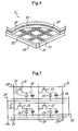
Fig. 4 is a perspective view showing a general configuration of the reflection type liquid crystal display apparatus according to the present invention. -
Fig. 5 is a connection view showing a circuit configuration of the reflection type liquid crystal display apparatus according to the present invention. -
Fig. 6 illustrates an embodiment of a reflection type liquid crystal projector according to the present invention. -
Fig. 7 is a sectional view showing a reflection type liquid crystal display apparatus according to the related art. -
Fig. 1 illustrates a first embodiment of the reflection type liquid crystal display apparatus according to the present invention which comprises as a semiconductor device portion a first embodiment of the semiconductor device according to the present invention. - The reflection type liquid crystal display apparatus 1 according to this embodiment has, as a whole, a configuration in which a
liquid crystal layer 33 is formed by injecting a liquid crystal between asemiconductor device portion 10 for constituting an active matrix drive portion and a countertransparent substrate 32 provided with a countertransparent electrode 31 functioning in common for each pixel. - The
semiconductor device portion 10 has a configuration in which aswitching transistor 13 and asignal accumulation capacitor 15 are formed on a semiconductor substrate (semiconductor base) 11 such as a silicon substrate of a first conduction type, for example, P type, on the basis of each unit region for constituting a pixel Px. - The
switching transistor 13 is constituted as a MIS type or MOS type transistor in which a source region 13S and adrain region 13D of a second conduction type (namely, of N type where the semiconductor substrate 11 is of P type) are formed in the semiconductor substrate 11, and agate electrode 13G formed of polysilicon or the like is formed on the region between the source region 13S and thedrain region 13D, with athin insulating layer 12a therebetween which constitutes a part of aninsulating layer 12 formed of silicon dioxide or the like. - The
signal accumulation capacitor 15 is constituted as a MIS type or MOS type transistor in which high-concentration semiconductor regions electrode 15G is formed on the region between thesemiconductor regions insulating layer 12b therebetween which constitutes a part of theinsulating layer 12. With an appropriate potential impressed on thesemiconductor regions channel 15c is formed at a portion beneath theelectrode 15G between thesemiconductor regions - In this embodiment, further, a high-concentration
bias semiconductor region 17 of the same first conduction type as that of the semiconductor substrate 11 (namely, of P type where the semiconductor substrate 11 is of P type), for impressing a bias potential such as an earth potential on the semiconductor substrate 11, is formed in the semiconductor substrate 11 on the basis of each unit region for constituting the pixel Px. - Besides, on an insulating
layer 14 formed on the insulatinglayer 12, a scan line (scan electrode) 21 is formed in connection with thegate electrode 13G of the switchingtransistor 13, a signal line (signal electrode) 23 is formed in connection with the source region 13S of the switchingtransistor 13, awiring 25 is formed for interconnection between thedrain region 13D of the switchingtransistor 13 and theelectrode 15G of thesignal accumulation capacitor 15, and abias electrode 27 is formed in connection with thesemiconductor regions signal accumulation capacitor 15 and thebias semiconductor region 17. - Furthermore, on an insulating
layer 16 formed on the insulatinglayer 14, areflection electrode 19 for constituting a pixel electrode is formed in connection with thewiring 25, i.e., in connection with thedrain region 13D of the switchingtransistor 13 and theelectrode 15G of thesignal accumulation capacitor 15. - As shown in
Fig. 4 , the reflection type liquid crystal display apparatus 1 has a configuration in which a multiplicity ofscan lines 21 are arranged in a vertical direction of a display screen, a multiplicity ofsignal lines 23 are arranged in a horizontal direction of the display screen, and the portion of each of the intersections of thescan lines 21 and the signal lines 23 is constituted as a pixel Px as above-described. - As shown in
Fig. 5 , a drive circuit is so constituted that with thebias electrodes 27 earthed, with the earth potential impressed on thesemiconductor regions signal accumulation capacitors 15 and thebias semiconductor regions 17, and with a predetermined potential impressed on the countertransparent electrode 31 functioning in common for each pixel, thescan lines 21 are sequentially selected by a scan line drive circuit, and a predetermined potential is impressed on thegate electrode 13G of the switchingtransistor 13 for the pixel connected to thescan line 21 thus selected, whereby the switchingtransistor 13 for the pixel under consideration is turned ON, and a signal voltage is impressed on the source region 13S of the switchingtransistor 13 for the pixel under consideration through thesignal line 23 by a signal line drive circuit, whereby a signal charge is accumulated in the capacitance of thesignal accumulation capacitor 15 for the pixel under consideration through thedrain region 13D of the switchingtransistor 13 for the pixel under consideration. - The signal charge thus accumulated is impressed on the
reflection electrode 19 for the pixel under consideration, and an electric field according to the signal voltage is impressed between the countertransparent electrode 31 functioning in common for each pixel and thereflection electrode 19 for the pixel under consideration. According to this, the rotatory polarization state of the liquid crystal at the portion of the pixel under consideration having a liquid crystal capacity Cx of theliquid crystal layer 33 is controlled, and the light which is incident on the reflection type liquid crystal display apparatus 1 from the outside of the countertransparent substrate 32, is transmitted through the portion of the pixel under consideration of theliquid crystal layer 33, is reflected by thereflection electrode 19, is again transmitted through the portion of the pixel under consideration of theliquid crystal layer 33 and goes out to the outside of the countertransparent substrate 32 is modulated, and the light in a predetermined polarization direction is outputted, whereby an image is displayed on the reflection type liquid crystal display apparatus 1. - In the reflection type liquid crystal display apparatus 1 and the
semiconductor device portion 10 according to the embodiment shown inFig. 1 , thesemiconductor regions signal accumulation capacitor 15 are of the same conduction type as that of the semiconductor substrate (semiconductor base) 11, i.e., of the conduction type different from that of the source region 13S and thedrain region 13D of the switchingtransistor 13. Therefore, for separation between the switching transistor region and the signal accumulation capacitor region, the distance between the switching transistor region and the signal accumulation capacitor region, i.e., the distance d between thedrain region 13D of the switchingtransistor 13 and the semiconductor region 15D. of thesignal accumulation capacitor 15 can be made to be sufficiently small, whereby the area of the pixel Px can be reduced, and the number of pixels which can be formed in a predetermined size can be enlarged. - Moreover, not only the
bias semiconductor region 17 but also thesemiconductor regions signal accumulation capacitors 15 are used as the regions for impressing the bias potential on the semiconductor substrate 11; accordingly, the bias potential is stably impressed on the semiconductor substrate 11, and noise resistance is enhanced. - Incidentally, a bias potential different from the earth potential may be impressed on the
semiconductor regions signal accumulation capacitor 15 and thebias semiconductor region 17. - Besides, on the contrary to the embodiment shown in
Fig. 1 , the semiconductor substrate (semiconductor base) 11, thesemiconductor regions signal accumulation capacitor 15 and thebias semiconductor region 17 may be of N type, while the source region 13S and thedrain region 13D of the switchingtransistor 13 may be of P type. - Furthermore, instead of using the semiconductor substrate directly as the semiconductor base and forming the source region and the drain region of the switching transistor, the semiconductor regions for constituting the signal accumulation capacitor, and the bias semiconductor region in the semiconductor base, a configuration may be adopted in which, for example, a semiconductor base of P type is formed on a semiconductor substrate of N type, and a source region and a drain region of N type for constituting the switching transistor, a semiconductor region of P type for constituting the signal accumulation capacitor, and a bias semiconductor region of P type are formed in the semiconductor base of the P type.
-
Fig. 2 illustrates a second embodiment of the reflection type liquid crystal display apparatus according to the present invention which comprises as a semiconductor device portion a second embodiment of the semiconductor device according to the present invention. - In this embodiment, in the case of forming the switching
transistor 13 and thesignal accumulation capacitor 15 on the semiconductor substrate (semiconductor base) 11 as in the embodiment shown inFig. 1 , a bias semiconductor region is not formed in the semiconductor substrate 11 separately from the high-concentration semiconductor regions signal accumulation capacitor 15, and, instead, thesemiconductor regions signal accumulation capacitor 15 are made to serve also as the bias semiconductor region for impressing the bias potential on the semiconductor substrate 11. - Besides, a
bias electrode 27 is formed on the insulatinglayer 14 in the state of being connected to thesemiconductor regions bias electrode 27 is connected to a bias potential point such as an earth potential point, whereby a bias potential such as the earth potential is impressed on thesemiconductor regions Fig. 1 . - Therefore, in the embodiment shown in
Fig. 2 , like in the embodiment shown inFig. 1 , for separation between the switching transistor region and the signal accumulation capacitor region, the distance between the switching transistor region and the signal accumulation capacitor region, i.e., the distance between thedrain region 13D of the switchingtransistor 13 and thesemiconductor region 15D of thesignal accumulation capacitor 15 can be made to be sufficiently small. In addition, the portion for forming thebias semiconductor region 17 in the embodiment shown inFig. 1 can be cut from the pixel region. Therefore, as compared with the embodiment shown inFig. 1 , the area of the pixel Px can be further reduced, and the number of pixels which can be formed in a predetermined size can be further enlarged. - Moreover, the area of the pixel Px can be made to be sufficiently small, even without reducing the area of the
semiconductor regions signal accumulation capacitor 15 serving also as the bias semiconductor region. As a result, the bias potential is stably impressed on the semiconductor substrate 11, and noise resistance is enhanced. - Incidentally, on the contrary to the embodiment shown in
Fig. 2 , the semiconductor substrate (semiconductor base) 11 and thesemiconductor regions signal accumulation capacitor 15 may be of N type, while the source region 13S and thedrain region 13D of the switchingtransistor 13 may be of P type. - Moreover, instead of using the semiconductor substrate directly as the semiconductor base and forming the source region and the drain region of the switching transistor and the semiconductor regions for constituting the signal accumulation capacitors in the semiconductor base, a configuration may be adopted in which, for example, a semiconductor base of P type is formed on a semiconductor substrate of N type, and a source region and a drain region of N type for constituting the switching transistor and semiconductor regions of P type for constituting the signal accumulation capacitor are formed in the semiconductor base of the P type.
-
Fig. 3 illustrates a reflection type liquid crystal display apparatus not according to the present invention which comprises as a semiconductor device portion a semiconductor device not according to the present invention. - In this example useful for understanding the invention, the switching
transistor 13 is configured in the same manner as those in the embodiments shown inFigs. 1 and2 . However, unlike in the embodiments shown inFigs. 1 and2 , thesignal accumulation capacitor 15 has a configuration in which anelectrode 15G is formed on a region, adjacent to thedrain region 13D of the switchingtransistor 13, of the semiconductor substrate (semiconductor base) 11, with a thininsulating layer 12b therebetween which constitutes a part of the insulatinglayer 12. With an appropriate potential impressed on theelectrode 15G, achannel 15c is formed at a portion beneath theelectrode 15G adjacent to thedrain region 13D, and a capacitance is formed. - In this example useful for understanding the invention, further, a high-concentration
bias semiconductor region 17 of the same first conduction type as that of the semiconductor substrate 11 (namely, of P type where the semiconductor substrate 11 is of P type), for impressing a bias potential such as the earth potential on the semiconductor substrate 11, is formed in the semiconductor substrate 11 on the basis of each unit region for constituting a pixel Px. - Besides, on an insulating
layer 14 formed on the insulatinglayer 12, ascan line 21 is formed in connection with thegate electrode 13G of the switchingtransistor 13, asignal line 23 is formed in connection with the source region 13S of the switchingtransistor 13, and abias electrode 27 is formed in connection with theelectrode 15G of thesignal accumulation capacitor 15 and thebias semiconductor region 17. On an insulatinglayer 16 formed on the insulatinglayer 14, areflection electrode 19 for constituting a pixel electrode is formed in connection with thedrain region 13D of the switchingtransistor 13. - A drive circuit is so constituted that, as shown in
Fig. 5 , with thebias electrode 27 earthed, with the earth potential impressed on theelectrode 15G of thesignal accumulation capacitor 15 and thebias semiconductor region 17, and with a predetermined potential impressed on the countertransparent electrode 31 functioning in common for each pixel, thescan lines 21 are sequentially selected by a scan line drive circuit, and a predetermined potential is impressed on thegate electrode 13G of the switchingtransistor 13 for the pixel connected to thescan line 21 thus selected, whereby the switchingtransistor 13 for the pixel under consideration is turned ON, and a signal voltage is impressed on the source region 13S of the switchingtransistor 13 for the pixel under consideration through asignal line 23 by a signal line drive circuit, whereby a signal charge is accumulated in the capacitance of thesignal accumulation capacitor 15 for the pixel under consideration through thedrain region 13D of the switchingtransistor 13 for the pixel under consideration. - The signal charge thus accumulated is impressed on the
reflection electrode 19 for the pixel under consideration, whereby an image is displayed on the reflection type liquid crystal display apparatus 1, in the same manner as in the embodiments shown inFigs. 1 and2 . - In the reflection type liquid crystal display apparatus 1 and the
semiconductor device portion 10 according to the comparative example shown inFig. 3 constituted as above-described, a semiconductor region for constituting thesignal accumulation capacitor 15 is not formed in the semiconductor substrate 11 separately from thedrain region 13D of the switchingtransistor 13. Therefore, even though thebias semiconductor region 17 is formed on the semiconductor substrate 11, the area of the pixel Px can be reduced, and the number of pixels which can be formed in a predetermined size can be enlarged. - Incidentally, a bias potential different from the earth potential may be impressed on the
electrode 15G of thesignal accumulation capacitor 15 and thebias semiconductor region 17. In addition, bias potentials different from each other may be impressed respectively on theelectrode 15G and thebias semiconductor region 17. - Besides, on the contrary to the comparative example shown in
Fig. 3 , the semiconductor substrate (semiconductor base) 11 and thebias semiconductor region 17 may be of N type, while the source region 13S and thedrain region 13D of the switchingtransistor 13 may be of P type. - Furthermore, instead of using the semiconductor substrate directly as the semiconductor base and forming the source region and the drain region of the switching transistor and the bias semiconductor region in the semiconductor base, a configuration may be adopted in which, for example, a semiconductor base of P type is formed on a semiconductor substrate of N type, and a source region and a drain region of N type for constituting the switching transistor and a bias semiconductor region of P type are formed in the semiconductor base of the P type.
- The reflection type liquid crystal display apparatus according to the present invention, constituted as those in the above-described embodiments, can be used, for example, for a reflection type liquid crystal projector (projection type display apparatus).
-
Fig. 6 illustrates an embodiment of the reflection type liquid crystal projector according to the present invention, using the reflection type liquid crystal display apparatus according to the present invention. - In the reflection type liquid crystal projector 2 according to this embodiment, non-polarized white light as parallel rays having a uniform intensity distribution in a predetermined region on a plane orthogonal to the center of light beam is emitted from an illumination unit 3 comprising a white light source therein.
- The light beam thus emitted is incident on a polarized light beam splitter 4, where it is split into a light beam of S polarized light reflected by the polarized light beam splitter 4, and a light beam of P polarized light transmitted through the polarized light beam splitter 4. The light beam of S polarized light reflected by the polarized light beam splitter 4 is incident on a
red reflector 5, where red light in the light beam of S polarized light is reflected by thered reflector 5, whereas green light and blue light are transmitted through thered reflector 5. Further, the green light and blue light transmitted through thered reflector 5 are incident on ablue reflector 6, where the blue light is reflected by theblue reflector 6, whereas the green light is transmitted through theblue reflector 6. - Then, the red light reflected by the
red reflector 5 is incident on a reflection type liquid crystal display apparatus 1R for red, the green light transmitted through theblue reflector 6 is incident on a reflection type liquid crystal display apparatus 1G for green, and the blue light reflected by theblue reflector 6 is incident on a reflection type liquid crystal display apparatus 1B for blue. - The reflection type liquid crystal display apparatuses 1R, 1G, and 1B are each a reflection type liquid crystal display apparatus according to the present invention, which is constituted as in the embodiment shown in
Fig. 1 ,Fig. 2 or in the example useful for understanding the invention shown inFig. 3 , and in which image data are written by red, green, and blue picture signals (color signals), respectively. - The red light incident on the reflection type liquid crystal display apparatus 1R, the green light incident on the reflection type liquid crystal display apparatus 1G, and the blue light incident on the reflection type liquid crystal display apparatus 1B are modulated respectively by the reflection type liquid crystal display apparatuses 1R, 1G, and 1B based on the picture signals, are then reflected, and again combined with each other by the
red reflector 5 and theblue reflector 6. Of the modulated red, green, and blue light beams thus re-combined, the P polarized light component is transmitted through the polarized light beam splitter 4 as image light, which is enlargedly projected on a screen 8 by a projection lens 7. - In the reflection type liquid crystal projector 2 according to this embodiment, the area of each pixel in the reflection type liquid crystal display apparatuses 1R, 1G, and 1B can be reduced, and the number of pixels which can be formed in a predetermined size can be enlarged, as described above. Therefore, where the reflection type liquid crystal display apparatuses 1R, 1G, and 1B are manufactured in a predetermined size, the number of the pixels in the reflection type liquid crystal display apparatuses 1R, 1G, and 1B can be enlarged, and a high-resolution image can be projected on the screen 8. On the other hand, where the reflection type liquid crystal display apparatuses 1R, 1G, and 1B each comprise a predetermined number of pixels, the size of the reflection type liquid crystal display apparatuses 1R, 1G, and 1B can be reduced, and, hence, the size of the reflection type liquid crystal projector 2 can be reduced.
- Incidentally, the reflection type liquid crystal projector according to the present invention is not limited to the one shown in the figure. It suffices for the reflection type liquid crystal projector to comprise an illumination optical system for emitting the light from a white light source in the form of a light beam having a uniform intensity distribution in a predetermined region on a plane orthogonal to the center of the light beam, a decomposing optical system for splitting the thus emitted light beam into a plurality of color light beams such as red, green and blue light beams, reflection type liquid crystal display apparatuses according to the present invention on which the thus split color light beams are respectively incident, a combining optical system for combining color image light beams emitted from the reflection type liquid crystal display apparatuses for the colors, and a projection optical system for projecting the combined image light on a screen. Besides, the reflection type liquid crystal projector may be constituted by use of a single-plate reflection type liquid crystal display apparatus, in place of the decomposing optical system and the combining optical system. Furthermore, a back projection type may be constituted, instead of the front projection type as in the embodiment shown in
Fig. 6 . - As has been described above, according to the present invention, it is possible to realize a reduction in the area of each pixel without degrading noise resistance.
Claims (4)
- A semiconductor device comprising a switching transistor (13) and a signal accumulation capacitor (15) on a semiconductor base (11) of a first conduction type in each unit area constituting a pixel, wherein
said switching transistor (13) comprises a drain region (13D) and a source region (13S) connected to a signal line (23), both of which regions are of a second conduction type different from the first one and are formed in said semiconductor base (11), and a gate electrode (13G) formed on the semiconductor base (11) at a position between said source region (13S) and said drain region (13D), with an insulating layer (12a) arranged between the gate electrode (13G) and the semiconductor base (11), said gate electrode (13G) being connected to a scan line (21),
said signal accumulation capacitor (15) comprises two semiconductor regions (15D, 15S) of said first conduction type formed in said semiconductor base (11), and an electrode (15G) formed on the semiconductor base (11) at a position between said two semiconductor regions (15D, 15S), with an insulating layer (12G) arranged between the electrode (15G) of the signal accummulation capacitor (15) and the semiconductor base (11); and
a reflection electrode (19) for constituting a pixel electrode is formed so as to be connected to said drain region (13D) of said switching transistor (13) and said electrode (15G) of said signal accumulation capacitor (15),
wherein said two semiconductor regions (15D, 15S) of said signal accumulation capacitor (15) are connected to a bias electrode (27), and serve also as bias semiconductor regions of said semiconductor base (11). - A semiconductor device as set forth in claim 1, wherein
a further bias semiconductor region (17) of said first conduction type is formed in said semiconductor base (11), separately from said semiconductor regions (15D, 15S) of said signal accumulation capacitor (15). - A reflection type liquid crystal display apparatus (1) comprising a liquid crystal layer (33) formed between a surface provided with said reflection electrode (19) of a semiconductor device as set forth in any of claims 1 to 2, and a surface, provided with a counter transparent electrode (31) functioning in common for each pixel, of a counter transparent substrate (32) disposed opposite to said semiconductor device.
- reflection type liquid crystal projector comprising a reflection type liquid crystal display apparatus (1) as set forth in claim 3, arranged to modulate light emitted from light source (3) based on a picture signal by said reflection type liquid crystal display apparatus (1), and to project the light outputted through the modulation through a projection lens (7).
Applications Claiming Priority (3)
| Application Number | Priority Date | Filing Date | Title |
|---|---|---|---|
| JP2002169861 | 2002-06-11 | ||
| JP2002169861 | 2002-06-11 | ||
| PCT/JP2003/007408 WO2003104883A1 (en) | 2002-06-11 | 2003-06-11 | Semiconductor device, reflection type liquid crystal display device, and reflection type liquid crystal projector |
Publications (3)
| Publication Number | Publication Date |
|---|---|
| EP1513005A1 EP1513005A1 (en) | 2005-03-09 |
| EP1513005A4 EP1513005A4 (en) | 2007-02-14 |
| EP1513005B1 true EP1513005B1 (en) | 2010-04-07 |
Family
ID=29727748
Family Applications (1)
| Application Number | Title | Priority Date | Filing Date |
|---|---|---|---|
| EP03733360A Expired - Lifetime EP1513005B1 (en) | 2002-06-11 | 2003-06-11 | Semiconductor device, reflection type liquid crystal display device, and reflection type liquid crystal projector |
Country Status (8)
| Country | Link |
|---|---|
| US (1) | US7309877B2 (en) |
| EP (1) | EP1513005B1 (en) |
| KR (1) | KR100963815B1 (en) |
| CN (1) | CN100354741C (en) |
| AU (1) | AU2003242279B2 (en) |
| DE (1) | DE60332017D1 (en) |
| TW (1) | TWI229774B (en) |
| WO (1) | WO2003104883A1 (en) |
Families Citing this family (2)
| Publication number | Priority date | Publication date | Assignee | Title |
|---|---|---|---|---|
| CN100432759C (en) * | 2005-01-07 | 2008-11-12 | 友达光电股份有限公司 | Flat display panel with same signal delay and signal line structure thereof |
| US7286192B2 (en) * | 2005-06-07 | 2007-10-23 | Au Optronics Corporation | Transflective liquid crystal display |
Citations (1)
| Publication number | Priority date | Publication date | Assignee | Title |
|---|---|---|---|---|
| JPH1115021A (en) * | 1997-06-26 | 1999-01-22 | Seiko Epson Corp | Liquid crystal panel, liquid crystal panel substrate, electronic device, and projection display device |
Family Cites Families (17)
| Publication number | Priority date | Publication date | Assignee | Title |
|---|---|---|---|---|
| JPS55164876A (en) | 1979-06-08 | 1980-12-22 | Tokyo Shibaura Electric Co | Semiconductor memory device and liquid crystal display device using same |
| US4523189A (en) * | 1981-05-25 | 1985-06-11 | Fujitsu Limited | El display device |
| JPS61119072A (en) | 1984-11-15 | 1986-06-06 | Toshiba Corp | Semiconductor capacity device |
| JPS6210619A (en) * | 1985-07-09 | 1987-01-19 | Seiko Epson Corp | Active matrix panel |
| US5245452A (en) | 1988-06-24 | 1993-09-14 | Matsushita Electronics Corporation | Active matric drive liquid crystal display device using polycrystalline silicon pixel electrodes |
| JPH0656878B2 (en) | 1988-07-22 | 1994-07-27 | ローム株式会社 | Method for manufacturing CMOS semiconductor device |
| JP3666893B2 (en) * | 1993-11-19 | 2005-06-29 | 株式会社日立製作所 | Semiconductor memory device |
| JP2720862B2 (en) | 1995-12-08 | 1998-03-04 | 日本電気株式会社 | Thin film transistor and thin film transistor array |
| JPH1039332A (en) * | 1996-07-19 | 1998-02-13 | Seiko Epson Corp | Liquid crystal panel, substrate for liquid crystal panel, and projection display device |
| JP3541650B2 (en) * | 1996-10-22 | 2004-07-14 | セイコーエプソン株式会社 | Liquid crystal panel substrate, liquid crystal panel, electronic device using the same, and projection display device |
| JP3739523B2 (en) * | 1997-04-16 | 2006-01-25 | 富士写真フイルム株式会社 | Reflective two-dimensional matrix spatial light modulator |
| JP3663825B2 (en) | 1997-04-21 | 2005-06-22 | セイコーエプソン株式会社 | Liquid crystal panel, liquid crystal panel substrate, electronic device, and projection display device |
| JP3470586B2 (en) | 1997-06-25 | 2003-11-25 | 日本ビクター株式会社 | Method of manufacturing matrix substrate for display |
| JP3458382B2 (en) * | 1998-11-26 | 2003-10-20 | セイコーエプソン株式会社 | ELECTRO-OPTICAL DEVICE, MANUFACTURING METHOD THEREOF, AND ELECTRONIC DEVICE |
| TW525216B (en) * | 2000-12-11 | 2003-03-21 | Semiconductor Energy Lab | Semiconductor device, and manufacturing method thereof |
| JP2002207213A (en) * | 2001-01-11 | 2002-07-26 | Hitachi Ltd | Liquid crystal display device or display device using the same |
| US6825496B2 (en) * | 2001-01-17 | 2004-11-30 | Semiconductor Energy Laboratory Co., Ltd. | Light emitting device |
-
2003
- 2003-06-11 US US10/485,634 patent/US7309877B2/en not_active Expired - Lifetime
- 2003-06-11 AU AU2003242279A patent/AU2003242279B2/en not_active Ceased
- 2003-06-11 CN CNB038010941A patent/CN100354741C/en not_active Expired - Lifetime
- 2003-06-11 WO PCT/JP2003/007408 patent/WO2003104883A1/en not_active Ceased
- 2003-06-11 DE DE60332017T patent/DE60332017D1/en not_active Expired - Lifetime
- 2003-06-11 EP EP03733360A patent/EP1513005B1/en not_active Expired - Lifetime
- 2003-06-11 KR KR1020047002005A patent/KR100963815B1/en not_active Expired - Lifetime
- 2003-06-11 TW TW092115848A patent/TWI229774B/en not_active IP Right Cessation
Patent Citations (1)
| Publication number | Priority date | Publication date | Assignee | Title |
|---|---|---|---|---|
| JPH1115021A (en) * | 1997-06-26 | 1999-01-22 | Seiko Epson Corp | Liquid crystal panel, liquid crystal panel substrate, electronic device, and projection display device |
Also Published As
| Publication number | Publication date |
|---|---|
| DE60332017D1 (en) | 2010-05-20 |
| US7309877B2 (en) | 2007-12-18 |
| TWI229774B (en) | 2005-03-21 |
| EP1513005A4 (en) | 2007-02-14 |
| CN100354741C (en) | 2007-12-12 |
| WO2003104883A1 (en) | 2003-12-18 |
| AU2003242279B2 (en) | 2008-10-02 |
| TW200408896A (en) | 2004-06-01 |
| AU2003242279A1 (en) | 2003-12-22 |
| US20040232416A1 (en) | 2004-11-25 |
| KR100963815B1 (en) | 2010-06-16 |
| CN1556937A (en) | 2004-12-22 |
| EP1513005A1 (en) | 2005-03-09 |
| KR20050007286A (en) | 2005-01-17 |
Similar Documents
| Publication | Publication Date | Title |
|---|---|---|
| EP1174757B1 (en) | Reflective type liquid crystal display device | |
| KR100469109B1 (en) | Electro-optical device and production method thereof and electronic equipment | |
| EP0837447B1 (en) | Active matrix substrate for use in liquid crystal display | |
| TW400451B (en) | Liquid crystal display device | |
| US6127998A (en) | Matrix substrate, liquid-crystal device incorporating the matrix substrate, and display device incorporating the liquid-crystal device | |
| US3840695A (en) | Liquid crystal image display panel with integrated addressing circuitry | |
| US10120250B2 (en) | Electro-optical device, electrical apparatus | |
| US6836302B2 (en) | Active matrix substrate, electro-optical device and electronic equipment | |
| US8223093B2 (en) | Electro-optical device, electronic apparatus, and projection display | |
| JP2018146870A (en) | Electro-optical device and electronic apparatus | |
| EP1513005B1 (en) | Semiconductor device, reflection type liquid crystal display device, and reflection type liquid crystal projector | |
| JP2958828B2 (en) | Image reading / display device | |
| JP3564990B2 (en) | Electro-optical devices and electronic equipment | |
| JP4501362B2 (en) | Semiconductor device, reflective liquid crystal display device, and reflective liquid crystal projector | |
| US6235546B1 (en) | Method of forming an active matrix electro-optic display device with storage capacitors | |
| US11520198B2 (en) | Electro-optical device and electronic apparatus | |
| JP7409236B2 (en) | Electro-optical devices and electronic equipment | |
| JP2009071212A (en) | Semiconductor device, method for manufacturing semiconductor device, and electro-optical device | |
| JPH07128687A (en) | Active matrix type pannel device | |
| JP2008164668A (en) | Liquid crystal display element and its manufacturing method | |
| JP2000305105A (en) | Liquid crystal display device | |
| JP2021131508A (en) | Electro-optics and electronic devices | |
| JP2004246371A (en) | Electro-optical devices and electronic equipment | |
| JP2004144837A (en) | Reflective liquid crystal display element | |
| HK1009545A (en) | Matrix substrate with row and column drivers for use in liquid crystal display |
Legal Events
| Date | Code | Title | Description |
|---|---|---|---|
| PUAI | Public reference made under article 153(3) epc to a published international application that has entered the european phase |
Free format text: ORIGINAL CODE: 0009012 |
|
| 17P | Request for examination filed |
Effective date: 20040121 |
|
| AK | Designated contracting states |
Kind code of ref document: A1 Designated state(s): AT BE BG CH CY CZ DE DK EE ES FI FR GB GR HU IE IT LI LU MC NL PT RO SE SI SK TR |
|
| AX | Request for extension of the european patent |
Extension state: AL LT LV MK |
|
| DAX | Request for extension of the european patent (deleted) | ||
| RBV | Designated contracting states (corrected) |
Designated state(s): AT BE BG DE FR GB |
|
| A4 | Supplementary search report drawn up and despatched |
Effective date: 20070112 |
|
| RIC1 | Information provided on ipc code assigned before grant |
Ipc: G02F 1/1362 20060101AFI20070108BHEP Ipc: H01L 27/04 20060101ALI20070108BHEP Ipc: G02F 1/1368 20060101ALI20070108BHEP |
|
| 17Q | First examination report despatched |
Effective date: 20070323 |
|
| GRAP | Despatch of communication of intention to grant a patent |
Free format text: ORIGINAL CODE: EPIDOSNIGR1 |
|
| GRAS | Grant fee paid |
Free format text: ORIGINAL CODE: EPIDOSNIGR3 |
|
| GRAA | (expected) grant |
Free format text: ORIGINAL CODE: 0009210 |
|
| RBV | Designated contracting states (corrected) |
Designated state(s): DE FR GB |
|
| AK | Designated contracting states |
Kind code of ref document: B1 Designated state(s): DE FR GB |
|
| REG | Reference to a national code |
Ref country code: GB Ref legal event code: FG4D |
|
| REF | Corresponds to: |
Ref document number: 60332017 Country of ref document: DE Date of ref document: 20100520 Kind code of ref document: P |
|
| PLBE | No opposition filed within time limit |
Free format text: ORIGINAL CODE: 0009261 |
|
| STAA | Information on the status of an ep patent application or granted ep patent |
Free format text: STATUS: NO OPPOSITION FILED WITHIN TIME LIMIT |
|
| 26N | No opposition filed |
Effective date: 20110110 |
|
| PGFP | Annual fee paid to national office [announced via postgrant information from national office to epo] |
Ref country code: DE Payment date: 20120622 Year of fee payment: 10 |
|
| PGFP | Annual fee paid to national office [announced via postgrant information from national office to epo] |
Ref country code: FR Payment date: 20120705 Year of fee payment: 10 Ref country code: GB Payment date: 20120622 Year of fee payment: 10 |
|
| GBPC | Gb: european patent ceased through non-payment of renewal fee |
Effective date: 20130611 |
|
| REG | Reference to a national code |
Ref country code: DE Ref legal event code: R119 Ref document number: 60332017 Country of ref document: DE Effective date: 20140101 |
|
| REG | Reference to a national code |
Ref country code: FR Ref legal event code: ST Effective date: 20140228 |
|
| PG25 | Lapsed in a contracting state [announced via postgrant information from national office to epo] |
Ref country code: GB Free format text: LAPSE BECAUSE OF NON-PAYMENT OF DUE FEES Effective date: 20130611 Ref country code: DE Free format text: LAPSE BECAUSE OF NON-PAYMENT OF DUE FEES Effective date: 20140101 |
|
| PG25 | Lapsed in a contracting state [announced via postgrant information from national office to epo] |
Ref country code: FR Free format text: LAPSE BECAUSE OF NON-PAYMENT OF DUE FEES Effective date: 20130701 |