EP1174757B1 - Reflective type liquid crystal display device - Google Patents
Reflective type liquid crystal display device Download PDFInfo
- Publication number
- EP1174757B1 EP1174757B1 EP01116754A EP01116754A EP1174757B1 EP 1174757 B1 EP1174757 B1 EP 1174757B1 EP 01116754 A EP01116754 A EP 01116754A EP 01116754 A EP01116754 A EP 01116754A EP 1174757 B1 EP1174757 B1 EP 1174757B1
- Authority
- EP
- European Patent Office
- Prior art keywords
- liquid crystal
- light
- crystal display
- electrodes
- films
- Prior art date
- Legal status (The legal status is an assumption and is not a legal conclusion. Google has not performed a legal analysis and makes no representation as to the accuracy of the status listed.)
- Expired - Lifetime
Links
Images


Classifications
-
- G—PHYSICS
- G02—OPTICS
- G02F—OPTICAL DEVICES OR ARRANGEMENTS FOR THE CONTROL OF LIGHT BY MODIFICATION OF THE OPTICAL PROPERTIES OF THE MEDIA OF THE ELEMENTS INVOLVED THEREIN; NON-LINEAR OPTICS; FREQUENCY-CHANGING OF LIGHT; OPTICAL LOGIC ELEMENTS; OPTICAL ANALOGUE/DIGITAL CONVERTERS
- G02F1/00—Devices or arrangements for the control of the intensity, colour, phase, polarisation or direction of light arriving from an independent light source, e.g. switching, gating or modulating; Non-linear optics
- G02F1/01—Devices or arrangements for the control of the intensity, colour, phase, polarisation or direction of light arriving from an independent light source, e.g. switching, gating or modulating; Non-linear optics for the control of the intensity, phase, polarisation or colour
- G02F1/13—Devices or arrangements for the control of the intensity, colour, phase, polarisation or direction of light arriving from an independent light source, e.g. switching, gating or modulating; Non-linear optics for the control of the intensity, phase, polarisation or colour based on liquid crystals, e.g. single liquid crystal display cells
- G02F1/133—Constructional arrangements; Operation of liquid crystal cells; Circuit arrangements
- G02F1/136—Liquid crystal cells structurally associated with a semi-conducting layer or substrate, e.g. cells forming part of an integrated circuit
- G02F1/1362—Active matrix addressed cells
- G02F1/136209—Light shielding layers, e.g. black matrix, incorporated in the active matrix substrate, e.g. structurally associated with the switching element
-
- G—PHYSICS
- G02—OPTICS
- G02F—OPTICAL DEVICES OR ARRANGEMENTS FOR THE CONTROL OF LIGHT BY MODIFICATION OF THE OPTICAL PROPERTIES OF THE MEDIA OF THE ELEMENTS INVOLVED THEREIN; NON-LINEAR OPTICS; FREQUENCY-CHANGING OF LIGHT; OPTICAL LOGIC ELEMENTS; OPTICAL ANALOGUE/DIGITAL CONVERTERS
- G02F1/00—Devices or arrangements for the control of the intensity, colour, phase, polarisation or direction of light arriving from an independent light source, e.g. switching, gating or modulating; Non-linear optics
- G02F1/01—Devices or arrangements for the control of the intensity, colour, phase, polarisation or direction of light arriving from an independent light source, e.g. switching, gating or modulating; Non-linear optics for the control of the intensity, phase, polarisation or colour
- G02F1/13—Devices or arrangements for the control of the intensity, colour, phase, polarisation or direction of light arriving from an independent light source, e.g. switching, gating or modulating; Non-linear optics for the control of the intensity, phase, polarisation or colour based on liquid crystals, e.g. single liquid crystal display cells
- G02F1/133—Constructional arrangements; Operation of liquid crystal cells; Circuit arrangements
- G02F1/1333—Constructional arrangements; Manufacturing methods
- G02F1/1335—Structural association of cells with optical devices, e.g. polarisers or reflectors
-
- G—PHYSICS
- G02—OPTICS
- G02F—OPTICAL DEVICES OR ARRANGEMENTS FOR THE CONTROL OF LIGHT BY MODIFICATION OF THE OPTICAL PROPERTIES OF THE MEDIA OF THE ELEMENTS INVOLVED THEREIN; NON-LINEAR OPTICS; FREQUENCY-CHANGING OF LIGHT; OPTICAL LOGIC ELEMENTS; OPTICAL ANALOGUE/DIGITAL CONVERTERS
- G02F1/00—Devices or arrangements for the control of the intensity, colour, phase, polarisation or direction of light arriving from an independent light source, e.g. switching, gating or modulating; Non-linear optics
- G02F1/01—Devices or arrangements for the control of the intensity, colour, phase, polarisation or direction of light arriving from an independent light source, e.g. switching, gating or modulating; Non-linear optics for the control of the intensity, phase, polarisation or colour
- G02F1/13—Devices or arrangements for the control of the intensity, colour, phase, polarisation or direction of light arriving from an independent light source, e.g. switching, gating or modulating; Non-linear optics for the control of the intensity, phase, polarisation or colour based on liquid crystals, e.g. single liquid crystal display cells
- G02F1/133—Constructional arrangements; Operation of liquid crystal cells; Circuit arrangements
- G02F1/136—Liquid crystal cells structurally associated with a semi-conducting layer or substrate, e.g. cells forming part of an integrated circuit
- G02F1/1362—Active matrix addressed cells
- G02F1/136277—Active matrix addressed cells formed on a semiconductor substrate, e.g. of silicon
Definitions
- the present invention relates to a liquid crystal display device useful for a liquid crystal projector which illuminates a liquid crystal display element with light from a light source and projects images on the liquid crystal display element on a screen.
- a liquid crystal display device includes a liquid crystal display panel (also called a liquid crystal display element or a liquid crystal cell) composed of a pair of insulating substrates at least one of which is made of a transparent plate, a transparent plastic plate or the like, and a layer of liquid crystal composition (a liquid crystal layer) sandwiched between the insulating substrates.
- a liquid crystal display panel also called a liquid crystal display element or a liquid crystal cell
- the liquid crystal display devices are divided roughly into the simple-matrix type and the active matrix type.
- a picture element hereinafter a pixel
- a pixel is formed by selectively applying voltages to pixel-forming strip electrodes formed on both of the two insulating substrates of the liquid crystal display panel, and thereby changing the orientation of a portion of the liquid crystal molecules of the liquid crystal composition corresponding to the pixel.
- the liquid crystal display panel is provided with signal lines, pixel electrodes, reference voltage electrodes and active elements each associated with one of the pixel electrodes for pixel selection which are formed on one of the substrates, and a pixel is formed by selecting the active element associated with the pixel and thereby changing the orientation of the liquid crystal molecules present between a pixel electrode connected to the active element and the reference voltage electrode associated with the pixel electrode.
- the so-called vertical electric field type is employed in which an electric field for changing the orientation of the liquid crystal molecules is applied between an electrode disposed on one of a pair of opposing substrates and another electrode disposed on the other of the opposing substrates.
- the so-called horizontal electric field type also called IPS (In-Plane Switching) type
- liquid crystal display devices in which an electric field for changing the orientation of the liquid crystal molecules is applied in a direction approximately in parallel with the major surfaces of the opposing substrates.
- liquid crystal projectors have been in practical use.
- the liquid crystal projector illuminates a liquid crystal display element with light from a light source and projects images on the liquid crystal display element on a screen.
- Two types, a reflective type and a transmissive type, of liquid crystal display elements are usable for liquid crystal projectors.
- the reflective type liquid crystal display element is capable of being configured to make approximately the entire pixel area a useful reflective area, and consequently it has the advantages of small size, high definition display and high luminance over the transmissive type liquid crystal display element.
- a reflective liquid crystal display element is disclosed in US 5 978 056 , for example.
- This patent discloses a multilayer light blocking film, but does not disclose the arrangement of two light blocking films spaced from each other in the direction of their thickness.
- US 6081305 discloses a liquid crystal display device according to the preamble of claim 1.
- Liquid crystal projectors have problems regarding the miniaturization, and increasing the resolution and luminance. To solve these problems, the liquid crystal display element used for the liquid crystal projector needs to be further reduced in size, and further increased in resolution and luminance. In reducing the size and increasing the resolution and luminance of the transmissive type liquid crystal display element, it is inevitable that the ratio of the light-transmissive area to the entire area in one pixel (hereinafter the aperture ratio) is reduced considerably.
- the liquid crystal display device of the present invention comprises:
- FIG. 1 is a schematic cross-sectional view of a liquid crystal display element for explaining an embodiment of the liquid crystal display device in accordance with the present invention.
- reference numeral 100 denotes a liquid crystal display element
- 1 is a driving circuit substrate
- 2 is a transparent substrate
- 3 is a liquid crystal composition
- 4 are spacers.
- the spacers 4 establish a fixed cell gap d between the driving circuit substrate 1 and the transparent substrate 2 which sandwich the liquid crystal composition 3.
- Reference numeral 5 denotes a reflective electrode formed on the driving circuit substrate 1
- 6 is a counter electrode for applying a voltage across the liquid crystal composition 3 in cooperation with the reflective electrode
- 7 and 8 are orientation films for orientating liquid crystal molecules of the liquid crystal composition 3 in specified directions
- 30 are active elements for applying a voltage to the reflective electrode 5.
- Reference numeral 34 denotes source regions, 35 are drain regions, 36 are gate electrodes, 38 are insulating films, 39 are field oxide films for electrically insulating transistors from each other, 41 are first interlayer insulating films, 42 are first conductive films serving as drain signal lines, 43 are second interlayer insulating films, 44 are first light blocking films, 45 are third interlayer insulating films, 46 are second light blocking films, 47 are fourth interlayer insulating films, and 48 are second conductive films forming the reflective electrodes 5.
- the conductive film 42 are metal films made of aluminum.
- the second interlayer insulating films 43 insulate the first conductive films 42 from the first light blocking films 44.
- the second interlayer insulating films 43 are composed of planarizing films for flattening steps generated by structures on the driving circuit substrate 1 and insulating films covering the planarizing films, the planarizing films are coated by using an SOG (spin-on-glass) technique, and the insulating films are made of SiO 2 formed by a CVD technique using a reactive gas of TEOS (tetraethylorthosilicate).
- the second interlayer insulating films 43 are planarized by polishing using a CMP (Chemical Mechanical Polishing) technique after deposition of the second interlayer insulating films 43.
- CMP Chemical Mechanical Polishing
- the first light blocking films 44 are formed on the planarized second interlayer insulating films 43, and they are made of aluminum like the first conductive films 42.
- the third interlayer insulating films 45 and the fourth interlayer insulating films 47 are made of the same material as that of the second interlayer insulating films 43, and they are planarized by polishing using the CMP technique after deposition of the third and fourth interlayer insulating films 45, 47, respectively.
- the second light blocking films 46 and the reflective electrode 5 are made of aluminum like the first conductive film 42.
- the third interlayer insulating films 45 are used as dielectric films for obtaining electrostatic capacitances as explained subsequently, and their thickness is preferably in a range of from 150 nm to 450 nm, more preferably about 300 nm, considering their withstand voltage and increasing of their electrostatic capacitances by decreasing their thickness.
- the reflective type liquid crystal display element will be explained, and the active element 30 and the first and second light blocking films 44, 46 will be described subsequently.
- the liquid crystal display element in this embodiment is of the reflective type. Light projected into the liquid crystal display element 100 enters from the transparent substrate 2 (at the top of FIG. 1 ), then passes through the liquid crystal composition 3, then is reflected back by the reflective electrode 5, then passes through the liquid crystal composition 3 again, then passes through the transparent substrate 2, and leaves the liquid crystal display element 100.
- the reflective electrode 5 when the reflective electrode 5 is disposed on the surface of the driving circuit substrate 1 on its liquid crystal composition 3 side, an opaque substrate such as a silicon substrate can be used as the driving circuit substrate 1.
- This structure has advantages in that the active elements 30 and wiring can be disposed below the reflective electrodes 5, whereby the area of the reflective electrodes 5 can be increased, and consequently, a higher aperture ratio can be realized. Also this structure has the advantage of radiating heat generated by light projected into the liquid crystal display element 100 from the back surface of the driving circuit substrate 1.
- SPTN single-polarizer twisted nematic
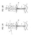
- Reference numeral 9 denotes a polarizing beam splitter which divides an incident light L1 from a light source (not shown) into two polarized lights, one thereof being linearly polarized light L2.
- the liquid crystal composition 3 is a nematic liquid crystal material having positive dielectric anisotropy.
- the longitudinal axes of the liquid crystal molecules are oriented approximately in parallel with the major surfaces of the driving circuit substrate 1 and the transparent substrate 2 (see FIG. 1 ), and the liquid crystal molecules are twisted across the liquid crystal layer by the orientation films 7, 8 (see FIG. 1 ).
- FIG. 2A illustrates a case where no voltage is applied across the layer of the liquid crystal composition 3.
- the light L2 entering the liquid crystal display element 100 is converted into elliptically polarized light by the birefringence of the liquid crystal composition 3, and then becomes approximately circularly polarized light on the reflective electrode 5.
- the light reflected by the reflective electrode 5 passes through the liquid crystal composition 3 again, thereby becomes elliptically polarized light again, and then returns to linearly polarized light again when it leaves the liquid crystal display element 100.
- the emergent linearly polarized light L3 is s-polarized light having its direction of polarization rotated through an angle of 90° with respect to that of the incident light L2, enters the polarizing beam splitter 9 again, and then is reflected by an internal interface of the polarizing beam splitter 9 to become emergent light L4 which in turn is projected onto a screen or the like to produce a display.
- This configuration is of the so-called normally white (normally open) type which emits light when a voltage is not applied across the layer of the liquid crystal composition 3.
- FIG. 2B illustrates the case where a voltage is applied across the layer of the liquid crystal composition 3.
- the liquid crystal molecules align in the direction of the electric field and consequently, the birefringence of the liquid crystal molecules does not appear.
- the linearly polarized light L2 entering the liquid crystal display element 100 is reflected by the reflective electrode 5 without undergoing changes, and then the light L5 emergent from the liquid crystal display element 100 has the same direction of polarization as that of the incident light L2.
- the emergent light L5 passes through the polarizing beam splitter 9, and returns to the light source such that no light is projected onto the screen and a black display is provided on the screen.
- the direction of orientation of the liquid crystal molecules is parallel with the major surfaces of the substrates, and therefore usual methods of orientating the liquid crystal molecules can be employed, and its manufacturing process is highly stable.
- the normally white mode operation is preventive of defective displays occurring at low voltage levels. The reason is that, in the normally white mode, a dark level (a black display) is provided when a high voltage is applied across the liquid crystal layer, and in this state, almost all the liquid crystal molecules are orientated in the direction of the electric field which is perpendicular to the major surfaces of the substrates, and consequently, the display of the dark level does not depend very much upon the initial conditions of orientation of the liquid crystal molecules having a low electric field applied thereto.
- the human eye perceives non-uniformity in luminance based upon the ratio of luminances, is responsive approximately to the logarithm of luminance, and consequently, is sensitive to variations in dark levels.
- the normally white mode has advantages with respect to prevention of non-uniformity in luminance caused by initial conditions of orientation of the liquid crystal molecules.
- the electrically controlled birefringence mode requires a highly precise cell gap between the substrates of the liquid crystal display element.
- the electrically controlled birefringence mode utilizes the phase difference between ordinary rays and extraordinary rays caused while they pass through the liquid crystal layer, and therefore the intensity of the light transmission through the liquid crystal layer depends upon the retardation ⁇ n • d between the ordinary and extraordinary rays, where ⁇ n is the birefringence and d is the cell gap established by spacers 4 between the transparent substrate 2 and the driving circuit substrate 1 (see FIG. 1 ).
- the cell gap d of the reflective type liquid crystal display element needs to be half that of the transmissive type liquid crystal display element.
- the cell gap d of the transmissive liquid crystal display element is in a range of about 5 to about 6 ⁇ m, and in this embodiment the cell gap d is selected to be about 2 ⁇ m.
- column-like spacers are fabricated on the driving circuit substrate 1 instead of using a bead-dispersing method.
- FIG. 3 is a schematic plan view of a liquid crystal display element for explaining the arrangement of the reflective electrodes 5 and the spacers 4 disposed on the driving circuit substrate 1.
- a large number of spacers 4 are arranged in a matrix array over the entire area of the driving circuit substrate 1 for establishing a uniform spacing between the transparent substrate 2 and the driving circuit substrate 1.
- Each of the reflective electrodes 5 defines a pixel serving as the smallest picture element formed by the liquid crystal display element.
- FIG. 3 illustrates an array of five columns by four rows of pixels, pixels in the outermost columns and rows are represented by reference numeral 5B, pixels within the outermost columns and rows are represented by reference numeral 5A.
- the array of five columns by four rows of pixels forms a display area, in which a display by the liquid crystal display element is formed.
- Dummy pixels 10 are disposed around the display area
- a peripheral frame 11 made of the same material as that of the spacers 4 is disposed around the dummy pixels 10
- a sealing member 12 is coated around the peripheral frame 11 on the driving circuit substrate 1.
- Reference numeral 13 denotes terminals for external connections which are used for supplying external signals to the liquid crystal display element 100.
- the spacers 4 and the peripheral frame 11 are formed of resin material.
- the liquid crystal composition 3 is placed between the driving circuit substrate 1 and the transparent substrate 2, and then is confined within a region enclosed by the peripheral frame 11 after the liquid crystal display element 100 has been assembled (see FIG. 1 ).
- a sealing member 12 is coated around the peripheral frame 11 on the driving circuit substrate 101 to seal the liquid crystal composition 3 off in the liquid crystal display element 100.
- the spacers 4 and the peripheral frame can be made of a resin material such as the chemically amplified negative photoresist "BPR-113" (a trade name) manufactured by JSR Corp. (Tokyo, Japan).
- the photoresist material is coated by a spin coating method on the driving circuit substrate 1 having the reflective electrodes 5 formed thereon, then is exposed through a mask having a pattern in the form of the spacers 4 and the peripheral frame 11, and then is developed by a remover to form the spacers 4 and the peripheral frame 11.
- the sealing member 12 serves to fix the driving circuit substrate 1 and the transparent substrate 2 together, and also serves to prevent materials harmful to the liquid crystal composition 3 from penetrating thereinto.
- the peripheral frame 11 serves as a stopper against the sealing member 12. Provision of the peripheral frame 11 serving as the stopper against the sealing member 12 makes it possible to define the border of the area of the liquid crystal composition 3 and that of the sealing member 12 accurately, and thereby to minimize the necessary inactive regions such as dummy pixels and a sealing region which do not contribute to the generation of a display and to reduce the size of the liquid crystal display element.
- This structure provides a wide latitude in design and thereby makes possible a reduction of the region between the display area and the peripheral sides of the liquid crystal display element 100, that is, a reduction of the peripheral border around the display area.
- the dummy pixels are disposed between the peripheral frame 11 and the display area for making the quality of the display produced by the outermost pixels 5B equal to that of the display produced by the pixels 5A disposed inside the outermost pixels 5B.
- the dummy pixels which do not contribute to the generation of a display, but are similar in structure to that of the pixels in the display area are provided at the peripheral areas surrounding the display area so as to prevent defective displays caused by structural discontinuity at the border between the display area and the peripheral areas surrounding the display area.
- the dummy pixels are also intended to prevent occurrence of defective displays in the so-called dot-inversion drive in which adjacent pixels have applied thereto driving voltages of opposite polarities from each other, and the polarities are inverted periodically.
- the pixels 5A disposed inside the outermost pixels 5B will be hereinafter referred to as the inner pixels 5A.
- the inner pixels 5A are pixels adjacent to each other, and therefore unwanted electric fields are generated between adjacent inner pixels 5A when the column-inversion, line-inversion or dot-inversion driving method is employed.
- the above-mentioned unwanted electric fields which deteriorate the display quality are not generated between the outermost pixels 5B and the areas on the side opposite from the inner pixels 5A when the dummy pixels 10 are not provided, and consequently, the outermost pixels 5B provide a display better in quality than that provided by the inner pixels 5A.
- the dummy electrodes 10 are provided to the liquid crystal display elements driven by the dot-inversion drive method, and are supplied with signals like the pixels 5A, 5B such that the display quality provided by the outermost pixels 5B is made equal to that provided by the inner pixels 5A.
- the column-inversion, the line-inversion or dot-inversion driving method is not employed, and therefore the problem of non-uniformity in the display does not arise which occurs with the column-inversion, line-inversion or dot-inversion driving.
- the liquid crystal display element of the present embodiment is driven in the normally white mode, a problem arises in that the dummy pixels 10 appear and degrade the display quality if no voltage is applied across the layer of the liquid crystal composition 3. It is conceivable to shield the dummy pixels 10 from light by using a light blocking border, but it is difficult to position the light blocking border accurately at the border of the display area.
- the dummy pixels 10 are supplied with such a voltage to make them produce a black display such that they are observed as a black border surrounding the display area.
- the width of the dummy pixels 10 disposed inside the peripheral frame 11 are selected to be equivalent to two or more lines of the regular pixels.
- FIG. 4 illustrates the dummy pixel 10D fabricated in the form of a peripheral frame, and the dummy pixel 10D is supplied with such a voltage to make it produce a black display.
- the dummy pixel 10 is shaped as a single electrode in the form of a peripheral frame as shown in FIG. 4 , a black display in the form of the peripheral frame is comparatively easily realized around the display area.
- the dummy pixel 10 shown in FIG. 4 produces a defective display at the border between the dummy pixel 10 and the display area.
- the liquid crystal composition 3 When an electric field is applied across the layer of the liquid crystal composition 3 in a fixed direction for a long period of time, the liquid crystal composition 3 is deteriorated, and in view of this phenomenon, a so-called AC driving method is known which inverts the polarities of the electric field applied across the layer of the liquid crystal composition 3 periodically.
- the frame-inversion drive method is employed which inverts the polarities of signals at all the pixels once per frame time, that is, with twice the frame time.
- signals of the same polarity are written into respective ones of the pixels for one frame time.
- writing of signals into the effective pixels in the display area is performed in the scanning order from the top row to the bottom row, and on the other hand, writing of a signal into the dummy pixel 10D is performed at one time because the dummy pixel 10D is in the form of a single electrode.
- a black-displaying signal (a high voltage if in the case of the normally white mode) is written into the respective effective pixels at positions from the upper left-hand corner to the lower right-hand corner of the display area sequentially within one frame time. If the black-displaying signal is written into the dummy pixel 10D at the same time the black-displaying signal is written into the effective pixel at the upper left-hand corner with both the black-displaying signals to the dummy pixel 10D and the effective pixels having the same polarity, a lateral electric field is generated between the effective pixel at the lower right-hand corner of the display area and the dummy pixel 10D during approximately the entire frame time, and lateral electric fields are generated between the outermost effective pixels and the dummy pixel 10D for a length of a time difference between times of writing the signals into the outermost effective pixels and the dummy pixel 10D.
- an unwanted lateral electric field produced by the black-displaying signal generates a locally white portion in a black background, that is, if a black display is intended over the entire display area, a white peripheral frame appears between the display area and the dummy pixel, and the brightness of the peripheral frame varies from place to place.
- FIGS. 5A-5C illustrate timing charts of video signals in the frame-inversion driving, and differences in the writing time will be explained with reference to FIGS. 5A-5C .
- a signal SE in FIG. 5B represents a video signal which is written into and stored in the pixels 5E in the first row in FIG. 4
- a signal SF in FIG. 5C represents a video signal supplied to the pixels 5F in the fourth line
- a signal SD represents a black-displaying signal supplied to the dummy pixel 10D
- Vcom in FIGS. 5A-5C represent a voltage applied to the counter electrode 6 (see FIG. 1 ).
- FIGS. 5A-5C illustrate a case in which a black-displaying signal is applied to all the pixels (an all-black display).
- the order of writing of video signals into the pixels sequentially is from the upper left-hand corner to the lower right-hand corner of the display area in the example shown in FIG. 4 , and therefore, first the black-displaying signals are written into the pixels in the first row sequentially, and then the black-displaying video signals are written in the pixels in the second row to the fourth row sequentially in the same way as in the first row.
- writing of the black-displaying signal into the dummy pixel 10D is performed simultaneously with writing of the signal into the pixels 5E in the first row.
- the polarity of the video signals in the first frame is positive with respect to the voltage Vcom
- the polarity of the video signals in the second frame is negative with respect to the voltage Vcom.
- the video signal SE is written in the pixels 5E at a time indicated by an arrow AE1, and then is held in the pixels 5E until a time indicated by an arrow AE2.
- the video signals are written into the pixels line by line from the top row to the bottom row, and therefore the video signals SF are written into the pixels 5F in the fourth row at a time indicated by an arrow AF1.
- the phase of the video signal SF written into the pixels 5F lags that of the black-displaying signal SD written into the dummy pixel 10D by approximately one frame time.
- the black-displaying signal SD and the video signal SF are opposite in polarity from each other for approximately one frame time, and therefore unwanted electric fields are generated between the pixels 5F and the dummy pixels 10D.
- the unwanted electric fields change the orientation of the molecules of the liquid crystal composition 3 such that locally somewhat white portions appear in a black display in the normally white mode, resulting in a non-uniform display.
- the present embodiment employs a structure in which a plurality of dummy pixels are provided such that dummy pixels in adjacent rows are separated from each other as shown in FIG. 3 .
- the black-displaying signal is written into each of the dummy pixels 10 simultaneously with the writing of signals into the effective pixels in a corresponding row.
- each of the dummy pixels 10 provided for each row of the effective pixels receives a signal of the same polarity as that of the signal written into the pixels of a corresponding row, and consequently, occurrence of the unwanted electric fields can be prevented, and non-uniformity in the display can be reduced.
- the dummy pixels 10 shown in FIG. 3 are laterally elongated compared with the effective pixels 5A and 5B.
- the liquid crystal display element 100 is provided with a light blocking frame for blocking unwanted light from illuminating portions other than the display area as described subsequently.
- the lateral elongation of the dummy pixels 10 provides a larger tolerance to the positioning accuracy of the light blocking frame in the liquid crystal display element 100.
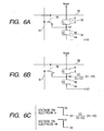
- FIGS. 6A-6C An equivalent circuit for one pixel is illustrated in FIGS. 6A and 6B in which the active element 30 is represented by a switch for clarity.
- Reference numeral 52 denotes a scanning signal line for supplying signals to turn the active element 30 ON or OFF, and 51 is a video signal line for supplying a video signal to be written into the pixel. As shown in FIGS.
- the reflective electrode 5 and the counter electrode 6 form a first capacitor 53
- the first light blocking film 44 and the second light blocking film 46 form a second capacitor 54.
- CL and CC the capacitances of the first capacitor 53 and the second capacitor 54 are denoted by CL and CC, respectively.
- the first light blocking film 44 serving as one electrode of the second capacitor 54 is supplied with a voltage V1 from some external source.
- a video signal V2 is supplied to the reflective electrode 5 and the second light blocking film 46.
- a voltage of negative polarity is produced by a voltage applied to the first light blocking film 44 with the reflective electrode 5 being supplied with a voltage of positive polarity, for example.
- This method for producing a voltage of negative polarity eliminates the need for supplying a voltage of negative polarity, and the peripheral circuits which have conventionally supplied signals of both positive and negative polarities can be configured to supply signals of only one of positive and negative polarities, making possible a low-voltage peripheral circuit and thereby making possible the formation of the peripheral circuit by using low-voltage rating components.
- the reflective electrodes 5 are spaced from each other with a specified gap therebetween to define the respective pixels.
- Light passes through the gaps, then enters a semiconductor layer of the active element 30, and generates charges (photocarriers) by photoelectric conversion.
- a portion of the photocarriers flow into the source region, change the video signal having been written into and stored in the reflective electrodes 5, and this is the so-called photoleak problem.
- a black matrix 20 made of light blocking films can be formed between the color filters 21.
- the black matrix 20 is formed so as to surround each of the pixels, and this means that the black matrix 20 is patterned to block light from illuminating the gaps between the reflective electrodes 5(48). Therefore, the black matrix 20 suffices for light blocking in the conventional liquid crystal display elements.
- the transparent substrate 2 is spaced from the driving circuit substrate 1, and consequently, the photoleak caused by light entering obliquely cannot be neglected when the intensity of the incident light is increased.
- liquid crystal projectors there is a type in which color splitting and recombination are performed outside the liquid crystal display element, and this type of liquid crystal display elements does not incorporate color filters thereinto, and therefore, it is not economical in view of the manufacturing steps to fabricate the black matrix 20 on the transparent substrate 2 for the purpose of light blocking only. Further, the employment of the black matrix 20 in the reflective liquid crystal display element causes the problem of reducing the aperture ratio.
- FIG. 8 illustrates the structure in which the light blocking films 44 are fabricated on the driving circuit substrate 1.
- the light blocking films 44 can be disposed closely to the semiconductor layer and block the obliquely incident light.
- Each of the light blocking films 44 can cover the entire area of a corresponding pixel, an opening to be made in the light blocking film 44 is only a contact hole 42CH for the electrical connection to the reflective electrode 5, and the amount of light incident on the semiconductor layer is reduced to be very small.
- the present inventors found out that flicker occurs in the display due to the leakage of light caused by the increased amount of light even in the structure of FIG. 8 . It is conceivable to prevent the problem of light leakage by reducing the size of the openings in the first light blocking films 44 and thereby decreasing the amount of light incident on the semiconductor layer, but in this embodiment second light blocking films are disposed below the openings in the reflective electrodes 5 as an alternative.
- the first and second light blocking films 44, 46 are disposed in the embodiments shown in FIGS. 1 and 9 .
- the connecting portion between the second light blocking film 46 and the first conductive film 42 has a structure in which a metal film forming the second light blocking film 46 and a metal film 44B made of the same metal as the first light blocking film 44 are laminated, but the second light blocking metal film 46 may be connected directly to the first conductive film 42.
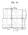
- FIG. 10 is a schematic plan view of the arrangement of the reflective electrodes 5 and the second light blocking films 46 viewed from the liquid crystal layer side with the orientation film being omitted for clarity.
- the second light blocking films 46 are disposed below the reflective electrodes 5 viewed from the liquid crystal layer side, light passes only through exposed portions 49 covered by none of the reflective electrodes 5 and the second light blocking films 46, and consequently, the amount of light incident on the semiconductor layer through the openings in the reflective electrodes 5 is greatly reduced.
- the size of the respective second light blocking films 46 is made approximately equal to that of the respective reflective electrodes 5, and therefore, the second light blocking films 46 are capable of covering most of the area of the openings 5P in the reflective electrodes 5.
- one reflective electrode 5 is about 8 ⁇ m in height and about 8 ⁇ m in width, and the gap between adjacent reflective electrodes 5 is 0.5 ⁇ m.
- Each of the reflective electrodes 5 is supplied with a video signal associated with a corresponding one of the pixels independently of others of the reflective electrodes 5 associated with others of the pixels, and therefore, the adjacent reflective electrodes 5 are separated from each other by openings 5P for electrical isolation.
- Each of the second light blocking films 46 is also supplied with a video signal associated with a corresponding one of the pixels independently of others of the second light blocking films 46, like the reflective electrodes 5, and therefore, the adjacent second light blocking films 46 are separated from each other by the openings 46P.
- Light can pass through the openings 5P and 46P provided for electrical isolation.
- the openings 5P in the reflective electrodes 5 are blocked up by the second light blocking film 46 so that light does not enter the semiconductor layer directly, and the openings 46P in the second light blocking films 46 are blocked up by the reflective electrodes 5 so that light does not enter the openings 46 directly. In this way the openings in one of the reflective electrodes 5 and the second light blocking films 46 are blocked up by the other of the reflective electrodes 5 and the second light blocking films 46 so as to enhance the light blocking effect.
- the openings 5P are not blocked up by the direct contact of the second light blocking films 46 with the openings 5P.
- the interlayer insulating film 47 is disposed between the reflective electrodes 5 and the second light blocking films 46 so as to insulate them from each other, and consequently, light can propagate in the interlayer insulating film 47.
- the first light blocking films 44 are provided to further prevent light from entering the semiconductor layer. Light can enter the semiconductor layer only through the openings 49, and therefore, the amount of light incident on the semiconductor layer is limited, but the provision of the first light blocking films 44 can prevent light more securely from entering the semiconductor layer.
- An opening to be formed in each of the first light blocking films 44 is a contact hole 42CH provided for each of the pixels. The first light blocking films 44 further block up the openings 49 causing light leakage which cannot be eliminated even by provision of the second light blocking film 46.
- the openings 49 causing light leakage can be blocked up directly by insulating materials.
- light blocking films can be formed on the light leakage openings 49 by using the same resin material as that of the spacers 4.
- the spacers 4 are disposed on the openings 49.
- the openings 5P in the reflective electrodes 5 can be blocked up by light blocking resin films.
- capacitors can be formed between the first and second light blocking films 44, 46.
- the second light blocking films 46 are supplied with the same video signals as those written into the reflective electrodes 5, and therefore, the capacitors can be used as the storage capacitances when a fixed voltage is applied to the first light blocking films 44.
- the second light blocking films 46 which are supplied with video signals function as second reflective electrodes also. As shown in FIG. 10 , the second light blocking films 46 are exposed in the openings 5P between the adjacent reflective electrodes 5, and therefore, the second light blocking films 46 can apply an electric field to the liquid crystal composition 3 via the fourth interlayer insulating film 47 and the orientation film 7 (see FIG. 1 ).
- the second light blocking films 46 are AC-driven in the same manner as the reflective electrodes 5 are, and therefore, the liquid crystal composition 3 in the vicinity of the openings 5P can be supplied with voltages whose polarity is inverted periodically, by the second light blocking films 46, and consequently, the application of electric fields in a fixed direction, i.e., DC fields, to the liquid crystal composition 3 in the vicinity of the openings 5P is prevented.
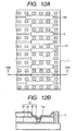
- FIGS. 12A and 12B illustrate a dummy pattern 14 formed around the external terminals 13.
- the pattern density of the area where the external terminals 13 are disposed is usually lower than that of the remainder of the driving circuit substrate 1.
- the amount of polishing depends upon the density of uneven structures (the pattern density) of the surface to be polished, and the flatness of the polished surface is degraded due to the unevenness.
- the dummy pattern 14 By disposing the dummy pattern 14 in an area around the external terminals 13 where the pattern density is low, the pattern density of the area around the external terminals is made uniform, and consequently, the subsequent chemical mechanical polishing makes possible a thin film having a uniformly flat surface.
- FIG. 12B is a cross-sectional view of the driving circuit substrate 1 taken along line XIIB-XIIB of FIG. 12A .
- the external terminal 13 is comprised of superposed layers of the first conductive film 42, the first light blocking film 44, the second light blocking film 46 and the reflective electrode 5.
- the conductive film in the connecting portion is composed of the three superposed layers of the first light blocking film 44, the second light blocking film 46 and the reflective electrode 5.
- the signal lines disposed within the driving circuits are made of the first conductive film 42, and therefore, the first light blocking film 44 and the first conductive film 42 are connected together via a contact hole made in the interlayer insulating film.
- FIG. 13 is a perspective view of the driving circuit substrate 1 superposed with the transparent substrate 2.
- the peripheral frame 11 Formed at the periphery of the driving circuit substrate 1 is the peripheral frame 11, and the liquid crystal composition 103 is confined in a space surrounded by the peripheral frame 11, the driving circuit substrate 1 and the transparent substrate 2.
- the sealing member 12 is coated around the outside of the peripheral frame 11 between the superposed driving circuit substrate 1 and the transparent substrate 2.
- the driving circuit substrate 1 and the transparent substrate 2 are fixed together by the sealing member 2 to form the liquid crystal display element (the liquid crystal display panel) 100.
- a flexible printed wiring board 80 for supplying external signals to the liquid crystal display element 100.
- Two outermost terminals on one end of the flexible printed wiring board 80 are made longer than the remainder of terminals to form counter-electrode terminals 81 to be connected to the counter electrode 6 formed on the transparent substrate 2.
- the flexible printed wiring board 80 is connected to both of the driving circuit substrate 1 and the transparent substrate 2.
- a flexible printed wiring board is connected to external terminals disposed on the driving circuit substrate 1, and therefore, the wiring to the counter electrode 6 from the flexible printed wiring board is made via the driving circuit substrate 1.
- the transparent substrate 2 in this embodiment of the present invention is provided with connecting portions 82 to be connected to the flexible printed wiring board 80 such that the flexible printed wiring board 80 is connected directly to the counter electrode 6.
- the liquid crystal display panel 100 is formed by superposing the transparent substrate 102 on the driving circuit substrate 101.
- the transparent substrate 2 is superposed on the driving circuit substrate 1 such that a peripheral portion of the transparent substrate 2 extends beyond the outside edges of the driving circuit substrate 1 and provides the connecting portions 82 where the flexible printed wiring board 80 is connected to the counter electrode 6.
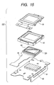
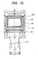
- FIGS. 15 , 16 and 17 illustrate the configuration of a liquid crystal display device 200.
- FIG. 15 is an exploded perspective view of the major elements of the liquid crystal display device 200
- FIG. 16 is a plan view of the liquid crystal display device 200
- FIG. 17 is a cross-sectional view of the liquid crystal display device of FIG. 16 .
- the thickness of the respective components is exaggerated for clarity.
- the liquid crystal display panel 100 having the flexible printed wiring board 80 connected thereto is disposed on the heat-radiating plate 62 with a cushion member 61 interposed therebetween.
- the cushion member 61 is highly heat-conductive, and fills the gap between the heat-radiating plate 62 and the liquid crystal display panel 100 for conducting heat from the liquid crystal display panel 100 to the heat-radiating plate 62 easily.
- Reference numeral 63 denotes a mold case, which is fixed to the heat-radiating plate 62 with an adhesive.
- the flexible printed wiring board 80 is passed between the mold case 63 and the heat-radiating plate 62, and then is brought out of the mold case 63.
- Reference numeral 65 denotes a light-blocking plate which prevents light from a light source from entering the unintended portions of the liquid crystal display device 200
- 66 is a light-blocking frame which is made of a glass plate and defines the display area of the liquid crystal display device 200.
- the present invention allows the realization of a reflective type liquid crystal display device useful for liquid crystal projectors to reduce their size, and to increase their resolution and luminance. Further, the present invention provides a high-display quality reflective type liquid crystal display device, and also a high-display quality liquid crystal display device and a liquid crystal projector employing it by preventing unwanted incident light from occurring in the liquid crystal display element.
Landscapes
- Physics & Mathematics (AREA)
- Nonlinear Science (AREA)
- Optics & Photonics (AREA)
- Crystallography & Structural Chemistry (AREA)
- Chemical & Material Sciences (AREA)
- General Physics & Mathematics (AREA)
- Mathematical Physics (AREA)
- Liquid Crystal (AREA)
- Engineering & Computer Science (AREA)
- Microelectronics & Electronic Packaging (AREA)
- Liquid Crystal Display Device Control (AREA)
- Optical Filters (AREA)
- Transforming Electric Information Into Light Information (AREA)
- Control Of Indicators Other Than Cathode Ray Tubes (AREA)
- Devices For Indicating Variable Information By Combining Individual Elements (AREA)
Description
- The present invention relates to a liquid crystal display device useful for a liquid crystal projector which illuminates a liquid crystal display element with light from a light source and projects images on the liquid crystal display element on a screen.
- Recently, liquid crystal display devices have been widely used in small-sized display devices, display terminals for office automation equipment and the like. Basically, a liquid crystal display device includes a liquid crystal display panel (also called a liquid crystal display element or a liquid crystal cell) composed of a pair of insulating substrates at least one of which is made of a transparent plate, a transparent plastic plate or the like, and a layer of liquid crystal composition (a liquid crystal layer) sandwiched between the insulating substrates.
- The liquid crystal display devices are divided roughly into the simple-matrix type and the active matrix type. In the simple-matrix type liquid crystal display device, a picture element (hereinafter a pixel) is formed by selectively applying voltages to pixel-forming strip electrodes formed on both of the two insulating substrates of the liquid crystal display panel, and thereby changing the orientation of a portion of the liquid crystal molecules of the liquid crystal composition corresponding to the pixel. On the other hand, in the active-matrix type liquid crystal display device, the liquid crystal display panel is provided with signal lines, pixel electrodes, reference voltage electrodes and active elements each associated with one of the pixel electrodes for pixel selection which are formed on one of the substrates, and a pixel is formed by selecting the active element associated with the pixel and thereby changing the orientation of the liquid crystal molecules present between a pixel electrode connected to the active element and the reference voltage electrode associated with the pixel electrode.
- Generally, in active matrix type liquid crystal display devices, the so-called vertical electric field type is employed in which an electric field for changing the orientation of the liquid crystal molecules is applied between an electrode disposed on one of a pair of opposing substrates and another electrode disposed on the other of the opposing substrates. Also put to practical use are the so-called horizontal electric field type (also called IPS (In-Plane Switching) type) liquid crystal display devices in which an electric field for changing the orientation of the liquid crystal molecules is applied in a direction approximately in parallel with the major surfaces of the opposing substrates.
- Among the display devices employing liquid crystal display devices, liquid crystal projectors have been in practical use. The liquid crystal projector illuminates a liquid crystal display element with light from a light source and projects images on the liquid crystal display element on a screen. Two types, a reflective type and a transmissive type, of liquid crystal display elements are usable for liquid crystal projectors. The reflective type liquid crystal display element is capable of being configured to make approximately the entire pixel area a useful reflective area, and consequently it has the advantages of small size, high definition display and high luminance over the transmissive type liquid crystal display element.
- Consequently, a small-sized high-definition liquid crystal projector can be realized by using the reflective liquid crystal display element without decreasing its luminance.
- A reflective liquid crystal display element is disclosed in
US 5 978 056 , for example. This patent discloses a multilayer light blocking film, but does not disclose the arrangement of two light blocking films spaced from each other in the direction of their thickness. -
US 6081305 discloses a liquid crystal display device according to the preamble ofclaim 1. - Liquid crystal projectors have problems regarding the miniaturization, and increasing the resolution and luminance. To solve these problems, the liquid crystal display element used for the liquid crystal projector needs to be further reduced in size, and further increased in resolution and luminance. In reducing the size and increasing the resolution and luminance of the transmissive type liquid crystal display element, it is inevitable that the ratio of the light-transmissive area to the entire area in one pixel (hereinafter the aperture ratio) is reduced considerably.
- It is an object of the present invention to provide a reflective liquid crystal display device capable of increasing its luminance, it is another object of the present invention to provide a reflective liquid crystal display element featuring a high image quality, and it is still another object to provide a liquid crystal display element featuring a high image quality by prevention of entering of unwanted light occurring therein and high light utilization efficiency obtained by a higher aperture ratio, and to provide a liquid crystal projector employing the liquid crystal display element.
- The above problems are solved in accordance with
claim 1. - The dependent claims relate to preferred embodiments of the present invention.
- The liquid crystal display device of the present invention comprises:
- a driving circuit substrate,
- a transparent substrate,
- a counter electrode provided with an orientation film on the transparent substrate,
- a plurality of reflective electrodes which define a pixel, being provided with an orientation film and arranged on the surface of the driving-circuit substrate on the liquid crystal layer side thereof and being adapted to be supplied with a video signal,
- a plurality of semiconductor switching elements disposed below the reflective electrodes, each being configured to supply video signals to a corresponding one of the plurality of reflective electrodes,
- spacers made of resin for establishing a fixed cell gap between the substrates,
- a liquid crystal layer sandwiched between the driving-circuit substrate and the transparent substrate,
and - a plurality of first and second light-blocking conductive films disposed to cover at least a portion of the spacings between adjacent reflective electrodes, the second light-blocking film being adapted to be supplied with the same video signals as the electrodes,
characterized in that - the first light-blocking films are disposed closely to the semiconductor layer of the driving-circuit substrate, each of the light blocking films covering the entire area of a corresponding pixel and having a contact hole for electrical connection to the reflective electrode,
- the second light-blocking films are disposed between the electrodes and the first light-blocking films and below the openings separating the electrodes, wherein the size of the second light-blocking film is approximately equal to that of the respective electrodes, and they are separated by openings blocked up by the electrodes,
- an interlayer insulating film is provided between the second light-blocking films and the electrodes,
- the spacers are disposed on the openings of the second light-blocking films,
- light-blocking films made of the same resin material as the spacers are provided on the openings,
- each of the plurality of second light-blocking films forms a capacitance with the first light-blocking film,
and - the polarity of the video voltage supplied to each of the plurality of second light-blocking films is inverted with respect to the voltage applied on the counter electrode at specified time intervals.
- In the accompanying drawings, like reference numerals designate similar components throughout the figures, and in which:
-
FIG. 1 is a schematic cross-sectional view of a liquid crystal display element for explaining an embodiment of the liquid crystal display device in accordance with the present invention; -
FIGS. 2A and 2B are illustrations of a liquid crystal display element of the electrically controlled birefringence mode for explaining an embodiment of the liquid crystal display device in accordance with the present invention; -
FIG. 3 is a schematic plan view of a liquid crystal display element for explaining an embodiment of the liquid crystal display device in accordance with the present invention; -
FIG. 4 is a schematic plan view of a liquid crystal display element for explaining an embodiment of the liquid crystal display device in accordance with the present invention; -
FIGS. 5A-5C are timing charts for explaining the operation of a liquid crystal display element in an embodiment of the liquid crystal display device in accordance with the present invention; -
FIGS. 6A and 6B are schematic equivalent circuits for explaining the operation of a liquid crystal display element in an embodiment of the liquid crystal display device in accordance with the present invention, andFIG. 6C shows the voltage relationship between electrodes of the liquid crystal display element; -
FIG. 7 is a schematic cross-sectional view of a liquid crystal display element for explaining an embodiment of the liquid crystal display device in accordance with the present invention; -
FIG. 8 is a schematic cross-sectional view of a liquid crystal display element for explaining an embodiment of the liquid crystal display device in accordance with the present invention; -
FIG. 9 is a schematic cross-sectional view of a liquid crystal display element for explaining an embodiment of the liquid crystal display device in accordance with the present invention; -
FIG. 10 is a schematic plan view of a liquid crystal display element for explaining an embodiment of the liquid crystal display device in accordance with the present invention; -
FIG. 11 is a schematic plan view of a liquid crystal display element for explaining an embodiment of the liquid crystal display device in accordance with the present invention; -
FIG. 12A is a schematic plan view of a terminal portion of a liquid crystal display element for explaining an embodiment of the liquid crystal display device in accordance with the present invention, andFIG. 12B is a cross-sectional view of the liquid crystal display element taken along line XIIB-XIIB ofFIG. 12A ; -
FIG. 13 is a schematic perspective view of an assembled liquid crystal display element for explaining an embodiment of the liquid crystal display device in accordance with the present invention; -
FIG. 14 is a schematic plan view of a liquid crystal display element for explaining an embodiment of the liquid crystal display device in accordance with the present invention; -
FIG. 15 is an exploded perspective view of an embodiment of the liquid crystal display device in accordance with the present invention; -
FIG. 16 is a schematic plan view of an embodiment of the liquid crystal display device in accordance with the present invention, and -
FIG. 17 is a schematic cross-sectional view of the liquid crystal display device ofFIG. 16 . - The embodiments in accordance with the present invention will now be explained in detail with reference to the drawings.
-
FIG. 1 is a schematic cross-sectional view of a liquid crystal display element for explaining an embodiment of the liquid crystal display device in accordance with the present invention. - In
FIG. 1 ,reference numeral 100 denotes a liquid crystal display element, 1 is a driving circuit substrate, 2 is a transparent substrate, 3 is a liquid crystal composition, 4 are spacers. Thespacers 4 establish a fixed cell gap d between the drivingcircuit substrate 1 and thetransparent substrate 2 which sandwich theliquid crystal composition 3.Reference numeral 5 denotes a reflective electrode formed on thedriving circuit substrate liquid crystal composition 3 in cooperation with thereflective electrode liquid crystal composition 3 in specified directions, and 30 are active elements for applying a voltage to thereflective electrode 5. -
Reference numeral 34 denotes source regions, 35 are drain regions, 36 are gate electrodes, 38 are insulating films, 39 are field oxide films for electrically insulating transistors from each other, 41 are first interlayer insulating films, 42 are first conductive films serving as drain signal lines, 43 are second interlayer insulating films, 44 are first light blocking films, 45 are third interlayer insulating films, 46 are second light blocking films, 47 are fourth interlayer insulating films, and 48 are second conductive films forming thereflective electrodes 5. - The
conductive film 42 are metal films made of aluminum. The secondinterlayer insulating films 43 insulate the firstconductive films 42 from the firstlight blocking films 44. The secondinterlayer insulating films 43 are composed of planarizing films for flattening steps generated by structures on thedriving circuit substrate 1 and insulating films covering the planarizing films, the planarizing films are coated by using an SOG (spin-on-glass) technique, and the insulating films are made of SiO2 formed by a CVD technique using a reactive gas of TEOS (tetraethylorthosilicate). The secondinterlayer insulating films 43 are planarized by polishing using a CMP (Chemical Mechanical Polishing) technique after deposition of the secondinterlayer insulating films 43. - The first
light blocking films 44 are formed on the planarized secondinterlayer insulating films 43, and they are made of aluminum like the firstconductive films 42. - The third
interlayer insulating films 45 and the fourthinterlayer insulating films 47 are made of the same material as that of the secondinterlayer insulating films 43, and they are planarized by polishing using the CMP technique after deposition of the third and fourthinterlayer insulating films - The second
light blocking films 46 and thereflective electrode 5 are made of aluminum like the firstconductive film 42. The thirdinterlayer insulating films 45 are used as dielectric films for obtaining electrostatic capacitances as explained subsequently, and their thickness is preferably in a range of from 150 nm to 450 nm, more preferably about 300 nm, considering their withstand voltage and increasing of their electrostatic capacitances by decreasing their thickness. - First, the reflective type liquid crystal display element will be explained, and the
active element 30 and the first and secondlight blocking films - The liquid crystal display element in this embodiment is of the reflective type. Light projected into the liquid
crystal display element 100 enters from the transparent substrate 2 (at the top ofFIG. 1 ), then passes through theliquid crystal composition 3, then is reflected back by thereflective electrode 5, then passes through theliquid crystal composition 3 again, then passes through thetransparent substrate 2, and leaves the liquidcrystal display element 100. - In the liquid crystal display element of the reflective type, when the
reflective electrode 5 is disposed on the surface of the drivingcircuit substrate 1 on itsliquid crystal composition 3 side, an opaque substrate such as a silicon substrate can be used as the drivingcircuit substrate 1. This structure has advantages in that theactive elements 30 and wiring can be disposed below thereflective electrodes 5, whereby the area of thereflective electrodes 5 can be increased, and consequently, a higher aperture ratio can be realized. Also this structure has the advantage of radiating heat generated by light projected into the liquidcrystal display element 100 from the back surface of the drivingcircuit substrate 1. - Next, the operation of the liquid crystal display element employing the electrically controlled birefringence mode will be explained. Light linearly polarized by a polarizer enters the liquid
crystal display element 100. When a voltage is applied between thereflective electrode 5 and thecounter electrode 6, the orientation of liquid crystal molecules of theliquid crystal composition 3 is changed due to their dielectric anisotropy, and as a result the birefringence of the layer of theliquid crystal composition 3 is changed. The electrically controlled birefringence mode generates images by converting the changes of the birefringence into changes of light transmission. - Next, the single-polarizer twisted nematic (SPTN) mode, which is one type of the electrically controlled birefringence mode, will be explained with reference to
FIGS. 2A and 2B . -
Reference numeral 9 denotes a polarizing beam splitter which divides an incident light L1 from a light source (not shown) into two polarized lights, one thereof being linearly polarized light L2. - In
FIGS. 2A and 2B , light having passed through thepolarizing beam splitter 9, which is a p-polarized light, enters into the liquidcrystal display element 100, but instead light reflected by thepolarizing beam splitter 9, which is an s-polarized light, can not enter into the liquidcrystal display element 100. - The
liquid crystal composition 3 is a nematic liquid crystal material having positive dielectric anisotropy. The longitudinal axes of the liquid crystal molecules are oriented approximately in parallel with the major surfaces of the drivingcircuit substrate 1 and the transparent substrate 2 (seeFIG. 1 ), and the liquid crystal molecules are twisted across the liquid crystal layer by theorientation films 7, 8 (seeFIG. 1 ). -
FIG. 2A illustrates a case where no voltage is applied across the layer of theliquid crystal composition 3. The light L2 entering the liquidcrystal display element 100 is converted into elliptically polarized light by the birefringence of theliquid crystal composition 3, and then becomes approximately circularly polarized light on thereflective electrode 5. The light reflected by thereflective electrode 5 passes through theliquid crystal composition 3 again, thereby becomes elliptically polarized light again, and then returns to linearly polarized light again when it leaves the liquidcrystal display element 100. The emergent linearly polarized light L3 is s-polarized light having its direction of polarization rotated through an angle of 90° with respect to that of the incident light L2, enters thepolarizing beam splitter 9 again, and then is reflected by an internal interface of thepolarizing beam splitter 9 to become emergent light L4 which in turn is projected onto a screen or the like to produce a display. This configuration is of the so-called normally white (normally open) type which emits light when a voltage is not applied across the layer of theliquid crystal composition 3. -
FIG. 2B illustrates the case where a voltage is applied across the layer of theliquid crystal composition 3. When an electric field is applied across the layer of theliquid crystal composition 3, the liquid crystal molecules align in the direction of the electric field and consequently, the birefringence of the liquid crystal molecules does not appear. As a result, the linearly polarized light L2 entering the liquidcrystal display element 100 is reflected by thereflective electrode 5 without undergoing changes, and then the light L5 emergent from the liquidcrystal display element 100 has the same direction of polarization as that of the incident light L2. The emergent light L5 passes through thepolarizing beam splitter 9, and returns to the light source such that no light is projected onto the screen and a black display is provided on the screen. - In the single-polarizer twisted nematic mode, the direction of orientation of the liquid crystal molecules is parallel with the major surfaces of the substrates, and therefore usual methods of orientating the liquid crystal molecules can be employed, and its manufacturing process is highly stable. The normally white mode operation is preventive of defective displays occurring at low voltage levels. The reason is that, in the normally white mode, a dark level (a black display) is provided when a high voltage is applied across the liquid crystal layer, and in this state, almost all the liquid crystal molecules are orientated in the direction of the electric field which is perpendicular to the major surfaces of the substrates, and consequently, the display of the dark level does not depend very much upon the initial conditions of orientation of the liquid crystal molecules having a low electric field applied thereto.
- The human eye perceives non-uniformity in luminance based upon the ratio of luminances, is responsive approximately to the logarithm of luminance, and consequently, is sensitive to variations in dark levels.
- Because of the above reasons, the normally white mode has advantages with respect to prevention of non-uniformity in luminance caused by initial conditions of orientation of the liquid crystal molecules.
- The electrically controlled birefringence mode requires a highly precise cell gap between the substrates of the liquid crystal display element. The electrically controlled birefringence mode utilizes the phase difference between ordinary rays and extraordinary rays caused while they pass through the liquid crystal layer, and therefore the intensity of the light transmission through the liquid crystal layer depends upon the retardation Δn • d between the ordinary and extraordinary rays, where Δn is the birefringence and d is the cell gap established by
spacers 4 between thetransparent substrate 2 and the driving circuit substrate 1 (seeFIG. 1 ). - In the reflective type liquid crystal display element, light entering the liquid crystal layer is reflected by the reflective electrode, and then passes through the liquid crystal layer again, therefore, if the reflective type liquid crystal display element uses a liquid crystal composition having the same birefringence Δn as that of a liquid crystal composition used in the transmissive type liquid crystal display element, the cell gap d of the reflective type liquid crystal display element needs to be half that of the transmissive type liquid crystal display element. Generally, the cell gap d of the transmissive liquid crystal display element is in a range of about 5 to about 6 µm, and in this embodiment the cell gap d is selected to be about 2 µm.
- In this embodiment, to ensure a high accuracy of the cell gap and a smaller cell gap than that of conventional liquid crystal display elements, column-like spacers are fabricated on the
driving circuit substrate 1 instead of using a bead-dispersing method. -
FIG. 3 is a schematic plan view of a liquid crystal display element for explaining the arrangement of thereflective electrodes 5 and thespacers 4 disposed on thedriving circuit substrate 1. A large number ofspacers 4 are arranged in a matrix array over the entire area of the drivingcircuit substrate 1 for establishing a uniform spacing between thetransparent substrate 2 and thedriving circuit substrate 1. Each of thereflective electrodes 5 defines a pixel serving as the smallest picture element formed by the liquid crystal display element. For the sake of simplicity,FIG. 3 illustrates an array of five columns by four rows of pixels, pixels in the outermost columns and rows are represented byreference numeral 5B, pixels within the outermost columns and rows are represented byreference numeral 5A. - In
FIG. 3 , the array of five columns by four rows of pixels forms a display area, in which a display by the liquid crystal display element is formed.Dummy pixels 10 are disposed around the display area, aperipheral frame 11 made of the same material as that of thespacers 4 is disposed around thedummy pixels 10, and a sealingmember 12 is coated around theperipheral frame 11 on thedriving circuit substrate 1.Reference numeral 13 denotes terminals for external connections which are used for supplying external signals to the liquidcrystal display element 100. - The
spacers 4 and theperipheral frame 11 are formed of resin material. Theliquid crystal composition 3 is placed between the drivingcircuit substrate 1 and thetransparent substrate 2, and then is confined within a region enclosed by theperipheral frame 11 after the liquidcrystal display element 100 has been assembled (seeFIG. 1 ). A sealingmember 12 is coated around theperipheral frame 11 on the driving circuit substrate 101 to seal theliquid crystal composition 3 off in the liquidcrystal display element 100. Thespacers 4 and the peripheral frame can be made of a resin material such as the chemically amplified negative photoresist "BPR-113" (a trade name) manufactured by JSR Corp. (Tokyo, Japan). The photoresist material is coated by a spin coating method on thedriving circuit substrate 1 having thereflective electrodes 5 formed thereon, then is exposed through a mask having a pattern in the form of thespacers 4 and theperipheral frame 11, and then is developed by a remover to form thespacers 4 and theperipheral frame 11. - The sealing
member 12 serves to fix thedriving circuit substrate 1 and thetransparent substrate 2 together, and also serves to prevent materials harmful to theliquid crystal composition 3 from penetrating thereinto. When thefluid sealing member 12 is applied, theperipheral frame 11 serves as a stopper against the sealingmember 12. Provision of theperipheral frame 11 serving as the stopper against the sealingmember 12 makes it possible to define the border of the area of theliquid crystal composition 3 and that of the sealingmember 12 accurately, and thereby to minimize the necessary inactive regions such as dummy pixels and a sealing region which do not contribute to the generation of a display and to reduce the size of the liquid crystal display element. This structure provides a wide latitude in design and thereby makes possible a reduction of the region between the display area and the peripheral sides of the liquidcrystal display element 100, that is, a reduction of the peripheral border around the display area. - The dummy pixels are disposed between the
peripheral frame 11 and the display area for making the quality of the display produced by theoutermost pixels 5B equal to that of the display produced by thepixels 5A disposed inside theoutermost pixels 5B. The dummy pixels which do not contribute to the generation of a display, but are similar in structure to that of the pixels in the display area are provided at the peripheral areas surrounding the display area so as to prevent defective displays caused by structural discontinuity at the border between the display area and the peripheral areas surrounding the display area. - The dummy pixels are also intended to prevent occurrence of defective displays in the so-called dot-inversion drive in which adjacent pixels have applied thereto driving voltages of opposite polarities from each other, and the polarities are inverted periodically.
- The
pixels 5A disposed inside theoutermost pixels 5B will be hereinafter referred to as theinner pixels 5A. By referring toFIG. 4 , the purpose of the dummy pixels will be explained. Theinner pixels 5A are pixels adjacent to each other, and therefore unwanted electric fields are generated between adjacentinner pixels 5A when the column-inversion, line-inversion or dot-inversion driving method is employed. On the other hand, the above-mentioned unwanted electric fields which deteriorate the display quality are not generated between theoutermost pixels 5B and the areas on the side opposite from theinner pixels 5A when thedummy pixels 10 are not provided, and consequently, theoutermost pixels 5B provide a display better in quality than that provided by theinner pixels 5A. The difference in display quality between some of the pixels produces non-uniformity in the display. Therefore, thedummy electrodes 10 are provided to the liquid crystal display elements driven by the dot-inversion drive method, and are supplied with signals like thepixels outermost pixels 5B is made equal to that provided by theinner pixels 5A. - In the present embodiment, the column-inversion, the line-inversion or dot-inversion driving method is not employed, and therefore the problem of non-uniformity in the display does not arise which occurs with the column-inversion, line-inversion or dot-inversion driving. However, when the liquid crystal display element of the present embodiment is driven in the normally white mode, a problem arises in that the
dummy pixels 10 appear and degrade the display quality if no voltage is applied across the layer of theliquid crystal composition 3. It is conceivable to shield thedummy pixels 10 from light by using a light blocking border, but it is difficult to position the light blocking border accurately at the border of the display area. In view of this, thedummy pixels 10 are supplied with such a voltage to make them produce a black display such that they are observed as a black border surrounding the display area. The width of thedummy pixels 10 disposed inside theperipheral frame 11 are selected to be equivalent to two or more lines of the regular pixels. -
FIG. 4 illustrates thedummy pixel 10D fabricated in the form of a peripheral frame, and thedummy pixel 10D is supplied with such a voltage to make it produce a black display. When thedummy pixel 10 is shaped as a single electrode in the form of a peripheral frame as shown inFIG. 4 , a black display in the form of the peripheral frame is comparatively easily realized around the display area. - However, it was found out that the
dummy pixel 10 shown inFIG. 4 produces a defective display at the border between thedummy pixel 10 and the display area. - When an electric field is applied across the layer of the
liquid crystal composition 3 in a fixed direction for a long period of time, theliquid crystal composition 3 is deteriorated, and in view of this phenomenon, a so-called AC driving method is known which inverts the polarities of the electric field applied across the layer of theliquid crystal composition 3 periodically. In this embodiment, the frame-inversion drive method is employed which inverts the polarities of signals at all the pixels once per frame time, that is, with twice the frame time. - In the frame-inversion drive method, signals of the same polarity are written into respective ones of the pixels for one frame time. In
FIG. 4 , writing of signals into the effective pixels in the display area is performed in the scanning order from the top row to the bottom row, and on the other hand, writing of a signal into thedummy pixel 10D is performed at one time because thedummy pixel 10D is in the form of a single electrode. As a result, some of the effective pixels have applied thereto signals of a polarity opposite from that of the signal applied to thedummy pixel 10D for a portion of the period depending upon the time of the period they are scanned, and consequently, effective lateral electric fields between thedummy pixels 10D and effective pixels adjacent thereto become non-uniform depending upon the positions of the effective pixels. A typical example of this phenomenon will now be explained with reference to the case of producing a black display over the entire display area. - In
FIG. 4 , a black-displaying signal (a high voltage if in the case of the normally white mode) is written into the respective effective pixels at positions from the upper left-hand corner to the lower right-hand corner of the display area sequentially within one frame time. If the black-displaying signal is written into thedummy pixel 10D at the same time the black-displaying signal is written into the effective pixel at the upper left-hand corner with both the black-displaying signals to thedummy pixel 10D and the effective pixels having the same polarity, a lateral electric field is generated between the effective pixel at the lower right-hand corner of the display area and thedummy pixel 10D during approximately the entire frame time, and lateral electric fields are generated between the outermost effective pixels and thedummy pixel 10D for a length of a time difference between times of writing the signals into the outermost effective pixels and thedummy pixel 10D. In the normally white mode, an unwanted lateral electric field produced by the black-displaying signal generates a locally white portion in a black background, that is, if a black display is intended over the entire display area, a white peripheral frame appears between the display area and the dummy pixel, and the brightness of the peripheral frame varies from place to place. -
FIGS. 5A-5C illustrate timing charts of video signals in the frame-inversion driving, and differences in the writing time will be explained with reference toFIGS. 5A-5C . A signal SE inFIG. 5B represents a video signal which is written into and stored in thepixels 5E in the first row inFIG. 4 , a signal SF inFIG. 5C represents a video signal supplied to thepixels 5F in the fourth line, a signal SD represents a black-displaying signal supplied to thedummy pixel 10D, and Vcom inFIGS. 5A-5C represent a voltage applied to the counter electrode 6 (seeFIG. 1 ). To facilitate understanding,FIGS. 5A-5C illustrate a case in which a black-displaying signal is applied to all the pixels (an all-black display). The order of writing of video signals into the pixels sequentially is from the upper left-hand corner to the lower right-hand corner of the display area in the example shown inFIG. 4 , and therefore, first the black-displaying signals are written into the pixels in the first row sequentially, and then the black-displaying video signals are written in the pixels in the second row to the fourth row sequentially in the same way as in the first row. On the other hand, writing of the black-displaying signal into thedummy pixel 10D is performed simultaneously with writing of the signal into thepixels 5E in the first row. The polarity of the video signals in the first frame is positive with respect to the voltage Vcom, and the polarity of the video signals in the second frame is negative with respect to the voltage Vcom. - In
FIGS. 5A-5C , the video signal SE is written in thepixels 5E at a time indicated by an arrow AE1, and then is held in thepixels 5E until a time indicated by an arrow AE2. The video signals are written into the pixels line by line from the top row to the bottom row, and therefore the video signals SF are written into thepixels 5F in the fourth row at a time indicated by an arrow AF1. The phase of the video signal SF written into thepixels 5F lags that of the black-displaying signal SD written into thedummy pixel 10D by approximately one frame time. As a result the black-displaying signal SD and the video signal SF are opposite in polarity from each other for approximately one frame time, and therefore unwanted electric fields are generated between thepixels 5F and thedummy pixels 10D. The unwanted electric fields change the orientation of the molecules of theliquid crystal composition 3 such that locally somewhat white portions appear in a black display in the normally white mode, resulting in a non-uniform display. - The above explanation has been made by referring to the
pixels 5F in the fourth row, but the pixels in the second and third rows are supplied with voltages opposite in polarity with respect to the voltage applied to thedummy pixel 10D, and consequently, a similar non-uniformity in the display is produced by the pixels in the second and third rows, but the degree of the non-uniformity varies depending upon the length of time for which the respective pixels are supplied with the voltages opposite in polarity with respect to the voltage applied to thedummy pixel 10D. - Returning to
FIG. 3 again, the embodiment of the present invention will be explained further. To prevent occurrence of non-uniformity caused by the structure of thedummy pixel 10D explained in connection withFIG. 4 , the present embodiment employs a structure in which a plurality of dummy pixels are provided such that dummy pixels in adjacent rows are separated from each other as shown inFIG. 3 . The black-displaying signal is written into each of thedummy pixels 10 simultaneously with the writing of signals into the effective pixels in a corresponding row. That is to say, each of thedummy pixels 10 provided for each row of the effective pixels receives a signal of the same polarity as that of the signal written into the pixels of a corresponding row, and consequently, occurrence of the unwanted electric fields can be prevented, and non-uniformity in the display can be reduced. - Further, the
dummy pixels 10 shown inFIG. 3 are laterally elongated compared with theeffective pixels crystal display element 100 is provided with a light blocking frame for blocking unwanted light from illuminating portions other than the display area as described subsequently. The lateral elongation of thedummy pixels 10 provides a larger tolerance to the positioning accuracy of the light blocking frame in the liquidcrystal display element 100. - The following explains a method for varying the voltage of the
reflective electrode 5 with respect to thecounter electrode 6 by application of a voltage to the firstlight blocking film 44 by using a capacitor formed between the first and secondlight blocking films FIG. 1 , with reference toFIGS. 6A-6C . An equivalent circuit for one pixel is illustrated inFIGS. 6A and 6B in which theactive element 30 is represented by a switch for clarity.Reference numeral 52 denotes a scanning signal line for supplying signals to turn theactive element 30 ON or OFF, and 51 is a video signal line for supplying a video signal to be written into the pixel. As shown inFIGS. 6A and 6B , thereflective electrode 5 and thecounter electrode 6 form afirst capacitor 53, and the firstlight blocking film 44 and the secondlight blocking film 46 form asecond capacitor 54. For simplicity, other parasitic capacitances are neglected, and the capacitances of thefirst capacitor 53 and thesecond capacitor 54 are denoted by CL and CC, respectively. - As shown in
FIGS. 6A and 6C , the firstlight blocking film 44 serving as one electrode of thesecond capacitor 54 is supplied with a voltage V1 from some external source. When theactive element 30 is turned ON by a scanning signal, a video signal V2 is supplied to thereflective electrode 5 and the secondlight blocking film 46. - Then, as shown in
FIGS. 6B and 6C , at the time theactive element 30 is turned OFF, the voltage applied to the firstlight blocking film 44 is changed from the voltage V1 to a voltage V3. As a result the voltage of thereflective electrode 5 and the secondlight blocking film 46 becomes V2 - CC/(CL + CC) x (VI - V3). - By using the above-explained method for varying the voltage of the
reflective electrode 5, a voltage of negative polarity is produced by a voltage applied to the firstlight blocking film 44 with thereflective electrode 5 being supplied with a voltage of positive polarity, for example. This method for producing a voltage of negative polarity eliminates the need for supplying a voltage of negative polarity, and the peripheral circuits which have conventionally supplied signals of both positive and negative polarities can be configured to supply signals of only one of positive and negative polarities, making possible a low-voltage peripheral circuit and thereby making possible the formation of the peripheral circuit by using low-voltage rating components. - Next, the first and second
light blocking films FIGS. 7-10 . - As shown in
FIG. 7 , thereflective electrodes 5 are spaced from each other with a specified gap therebetween to define the respective pixels. Light passes through the gaps, then enters a semiconductor layer of theactive element 30, and generates charges (photocarriers) by photoelectric conversion. A portion of the photocarriers flow into the source region, change the video signal having been written into and stored in thereflective electrodes 5, and this is the so-called photoleak problem. - When the intensity of light from the light source is small, a large portion of the light is reflected by the
reflective electrodes 5 which have the functions of reflecting light and shielding circuits underlying thereflective electrodes 5 from light, and consequently, light passing through the gaps does not cause a problem. - However, in a liquid crystal projector, strong light from the light source illuminates the liquid
crystal display element 100 to increase the luminance of the liquid crystal projector. Also there is a tendency that the display area of the liquid crystal display element decreases with decreasing size of the liquid crystal display element as the size of the liquid crystal projector is reduced, and as a result the illumination intensity on the display area of the liquid crystal display element is reduced further. Consequently, the photoleak cannot be prevented by the reflective electrodes 5(48) and therefore, the light blocking films need to be employed. - When color filters 21 are disposed on the
transparent substrate 2 as shown inFIG. 7 , ablack matrix 20 made of light blocking films can be formed between the color filters 21. Theblack matrix 20 is formed so as to surround each of the pixels, and this means that theblack matrix 20 is patterned to block light from illuminating the gaps between the reflective electrodes 5(48). Therefore, theblack matrix 20 suffices for light blocking in the conventional liquid crystal display elements. However, thetransparent substrate 2 is spaced from the drivingcircuit substrate 1, and consequently, the photoleak caused by light entering obliquely cannot be neglected when the intensity of the incident light is increased. - Among the liquid crystal projectors, there is a type in which color splitting and recombination are performed outside the liquid crystal display element, and this type of liquid crystal display elements does not incorporate color filters thereinto, and therefore, it is not economical in view of the manufacturing steps to fabricate the
black matrix 20 on thetransparent substrate 2 for the purpose of light blocking only. Further, the employment of theblack matrix 20 in the reflective liquid crystal display element causes the problem of reducing the aperture ratio. - As a solution to the above problems, in this embodiment of the present invention, light blocking films are formed on the
driving circuit substrate 1 by using process steps similar to those for fabrication of other metal layers in the liquid crystal display element.FIG. 8 illustrates the structure in which thelight blocking films 44 are fabricated on thedriving circuit substrate 1. Thelight blocking films 44 can be disposed closely to the semiconductor layer and block the obliquely incident light. Each of thelight blocking films 44 can cover the entire area of a corresponding pixel, an opening to be made in thelight blocking film 44 is only a contact hole 42CH for the electrical connection to thereflective electrode 5, and the amount of light incident on the semiconductor layer is reduced to be very small. - As described above, there was much progress in increasing the luminance of the liquid crystal projectors, however, there is still a demand for liquid crystal projectors for use even under normal room lighting conditions, and therefore the amount of light illuminating the liquid crystal display element from a light source has been increased.
- The present inventors found out that flicker occurs in the display due to the leakage of light caused by the increased amount of light even in the structure of
FIG. 8 . It is conceivable to prevent the problem of light leakage by reducing the size of the openings in the firstlight blocking films 44 and thereby decreasing the amount of light incident on the semiconductor layer, but in this embodiment second light blocking films are disposed below the openings in thereflective electrodes 5 as an alternative. - The first and second
light blocking films FIGS. 1 and9 . InFIG. 9 , the connecting portion between the secondlight blocking film 46 and the firstconductive film 42 has a structure in which a metal film forming the secondlight blocking film 46 and ametal film 44B made of the same metal as the firstlight blocking film 44 are laminated, but the second light blockingmetal film 46 may be connected directly to the firstconductive film 42. -
FIG. 10 is a schematic plan view of the arrangement of thereflective electrodes 5 and the secondlight blocking films 46 viewed from the liquid crystal layer side with the orientation film being omitted for clarity. As shown inFIG. 10 , the secondlight blocking films 46 are disposed below thereflective electrodes 5 viewed from the liquid crystal layer side, light passes only through exposedportions 49 covered by none of thereflective electrodes 5 and the secondlight blocking films 46, and consequently, the amount of light incident on the semiconductor layer through the openings in thereflective electrodes 5 is greatly reduced. The size of the respective secondlight blocking films 46 is made approximately equal to that of the respectivereflective electrodes 5, and therefore, the secondlight blocking films 46 are capable of covering most of the area of theopenings 5P in thereflective electrodes 5. As a dimensional example of an individualreflective electrode 5, onereflective electrode 5 is about 8 µm in height and about 8 µm in width, and the gap between adjacentreflective electrodes 5 is 0.5 µm. - Each of the
reflective electrodes 5 is supplied with a video signal associated with a corresponding one of the pixels independently of others of thereflective electrodes 5 associated with others of the pixels, and therefore, the adjacentreflective electrodes 5 are separated from each other byopenings 5P for electrical isolation. Each of the secondlight blocking films 46 is also supplied with a video signal associated with a corresponding one of the pixels independently of others of the secondlight blocking films 46, like thereflective electrodes 5, and therefore, the adjacent secondlight blocking films 46 are separated from each other by theopenings 46P. - Light can pass through the
openings openings 5P in thereflective electrodes 5 are blocked up by the secondlight blocking film 46 so that light does not enter the semiconductor layer directly, and theopenings 46P in the secondlight blocking films 46 are blocked up by thereflective electrodes 5 so that light does not enter theopenings 46 directly. In this way the openings in one of thereflective electrodes 5 and the secondlight blocking films 46 are blocked up by the other of thereflective electrodes 5 and the secondlight blocking films 46 so as to enhance the light blocking effect. - However, the
openings 5P are not blocked up by the direct contact of the secondlight blocking films 46 with theopenings 5P. Theinterlayer insulating film 47 is disposed between thereflective electrodes 5 and the secondlight blocking films 46 so as to insulate them from each other, and consequently, light can propagate in theinterlayer insulating film 47. In view of this, the firstlight blocking films 44 are provided to further prevent light from entering the semiconductor layer. Light can enter the semiconductor layer only through theopenings 49, and therefore, the amount of light incident on the semiconductor layer is limited, but the provision of the firstlight blocking films 44 can prevent light more securely from entering the semiconductor layer. An opening to be formed in each of the firstlight blocking films 44 is a contact hole 42CH provided for each of the pixels. The firstlight blocking films 44 further block up theopenings 49 causing light leakage which cannot be eliminated even by provision of the secondlight blocking film 46. - As shown in
FIG. 11 , theopenings 49 causing light leakage can be blocked up directly by insulating materials. For example, light blocking films can be formed on thelight leakage openings 49 by using the same resin material as that of thespacers 4. InFIG. 11 , thespacers 4 are disposed on theopenings 49. Further, theopenings 5P in thereflective electrodes 5 can be blocked up by light blocking resin films. - As described already, capacitors can be formed between the first and second
light blocking films light blocking films 46 are supplied with the same video signals as those written into thereflective electrodes 5, and therefore, the capacitors can be used as the storage capacitances when a fixed voltage is applied to the firstlight blocking films 44. The secondlight blocking films 46 which are supplied with video signals function as second reflective electrodes also. As shown inFIG. 10 , the secondlight blocking films 46 are exposed in theopenings 5P between the adjacentreflective electrodes 5, and therefore, the secondlight blocking films 46 can apply an electric field to theliquid crystal composition 3 via the fourthinterlayer insulating film 47 and the orientation film 7 (seeFIG. 1 ). The secondlight blocking films 46 are AC-driven in the same manner as thereflective electrodes 5 are, and therefore, theliquid crystal composition 3 in the vicinity of theopenings 5P can be supplied with voltages whose polarity is inverted periodically, by the secondlight blocking films 46, and consequently, the application of electric fields in a fixed direction, i.e., DC fields, to theliquid crystal composition 3 in the vicinity of theopenings 5P is prevented. - Next, a dummy pattern formed for making uniform the pattern density within a chip will be explained with reference to
FIGS. 12A and 12B. FIGS. 12A and 12B illustrate adummy pattern 14 formed around theexternal terminals 13. There are no structures other than theexternal terminals 13 disposed between the adjacent external terminals on thedriving circuit substrate 1 for prevention of electrical shorts in connecting the external terminals to an external circuit, and consequently, the pattern density of the area where theexternal terminals 13 are disposed is usually lower than that of the remainder of the drivingcircuit substrate 1. In chemical mechanical polishing, the amount of polishing depends upon the density of uneven structures (the pattern density) of the surface to be polished, and the flatness of the polished surface is degraded due to the unevenness. By disposing thedummy pattern 14 in an area around theexternal terminals 13 where the pattern density is low, the pattern density of the area around the external terminals is made uniform, and consequently, the subsequent chemical mechanical polishing makes possible a thin film having a uniformly flat surface. -
FIG. 12B is a cross-sectional view of the drivingcircuit substrate 1 taken along line XIIB-XIIB ofFIG. 12A . Theexternal terminal 13 is comprised of superposed layers of the firstconductive film 42, the firstlight blocking film 44, the secondlight blocking film 46 and thereflective electrode 5. To increase the thickness of a conductive film in the connecting portion, the conductive film in the connecting portion is composed of the three superposed layers of the firstlight blocking film 44, the secondlight blocking film 46 and thereflective electrode 5. The signal lines disposed within the driving circuits are made of the firstconductive film 42, and therefore, the firstlight blocking film 44 and the firstconductive film 42 are connected together via a contact hole made in the interlayer insulating film. -
FIG. 13 is a perspective view of the drivingcircuit substrate 1 superposed with thetransparent substrate 2. Formed at the periphery of the drivingcircuit substrate 1 is theperipheral frame 11, and the liquid crystal composition 103 is confined in a space surrounded by theperipheral frame 11, the drivingcircuit substrate 1 and thetransparent substrate 2. The sealingmember 12 is coated around the outside of theperipheral frame 11 between the superposeddriving circuit substrate 1 and thetransparent substrate 2. The drivingcircuit substrate 1 and thetransparent substrate 2 are fixed together by the sealingmember 2 to form the liquid crystal display element (the liquid crystal display panel) 100. - Next, as shown in
FIG. 14 , connected to theexternal terminals 13 is a flexible printedwiring board 80 for supplying external signals to the liquidcrystal display element 100. Two outermost terminals on one end of the flexible printedwiring board 80 are made longer than the remainder of terminals to formcounter-electrode terminals 81 to be connected to thecounter electrode 6 formed on thetransparent substrate 2. In this way, the flexible printedwiring board 80 is connected to both of the drivingcircuit substrate 1 and thetransparent substrate 2. - Conventionally, a flexible printed wiring board is connected to external terminals disposed on the
driving circuit substrate 1, and therefore, the wiring to thecounter electrode 6 from the flexible printed wiring board is made via thedriving circuit substrate 1. - The
transparent substrate 2 in this embodiment of the present invention is provided with connectingportions 82 to be connected to the flexible printedwiring board 80 such that the flexible printedwiring board 80 is connected directly to thecounter electrode 6. The liquidcrystal display panel 100 is formed by superposing the transparent substrate 102 on the driving circuit substrate 101. Thetransparent substrate 2 is superposed on thedriving circuit substrate 1 such that a peripheral portion of thetransparent substrate 2 extends beyond the outside edges of the drivingcircuit substrate 1 and provides the connectingportions 82 where the flexible printedwiring board 80 is connected to thecounter electrode 6. -
FIGS. 15 ,16 and17 illustrate the configuration of a liquidcrystal display device 200.FIG. 15 is an exploded perspective view of the major elements of the liquidcrystal display device 200,FIG. 16 is a plan view of the liquidcrystal display device 200, andFIG. 17 is a cross-sectional view of the liquid crystal display device ofFIG. 16 . InFIG. 17 , the thickness of the respective components is exaggerated for clarity. - As shown in
FIG. 15 , the liquidcrystal display panel 100 having the flexible printedwiring board 80 connected thereto is disposed on the heat-radiatingplate 62 with acushion member 61 interposed therebetween. Thecushion member 61 is highly heat-conductive, and fills the gap between the heat-radiatingplate 62 and the liquidcrystal display panel 100 for conducting heat from the liquidcrystal display panel 100 to the heat-radiatingplate 62 easily.Reference numeral 63 denotes a mold case, which is fixed to the heat-radiatingplate 62 with an adhesive. - As shown in
FIG. 17 , the flexible printedwiring board 80 is passed between themold case 63 and the heat-radiatingplate 62, and then is brought out of themold case 63.Reference numeral 65 denotes a light-blocking plate which prevents light from a light source from entering the unintended portions of the liquidcrystal display device crystal display device 200. - As explained above, the present invention allows the realization of a reflective type liquid crystal display device useful for liquid crystal projectors to reduce their size, and to increase their resolution and luminance. Further, the present invention provides a high-display quality reflective type liquid crystal display device, and also a high-display quality liquid crystal display device and a liquid crystal projector employing it by preventing unwanted incident light from occurring in the liquid crystal display element.
Claims (4)
- Liquid crystal display device, comprising:- a driving circuit substrate (1),- a transparent substrate (2),- a counter electrode (6) provided with an orientation film (8) on the transparent substrate (2),- a plurality of reflective electrodes (5) which define a pixel, being provided with an orientation film (7) and arranged on the surface of the driving-circuit substrate (1) on the liquid crystal layer side thereof and being adapted to be supplied with a video signal,- a plurality of semiconductor switching elements (34, 35, 36, 38, 39) disposed below the reflective electrodes (5), each being configured to supply video signals to a corresponding one of the plurality of reflective electrodes (5),- spacers (4) made of resin for establishing a fixed cell gap (d) between the substrates (1, 2),- a liquid crystal layer (3) sandwiched between the driving-circuit substrate (1) and the transparent substrate (2),
and- a plurality of first and second light-blocking conductive films (44, 46) disposed to cover at least a portion of the spacings between adjacent reflective electrodes, the second light-blocking film (46) being adapted to be supplied with the same video signals as the electrodes (5),characterized in that- the first light-blocking films (44) are disposed closely to the semiconductor layer of the driving-circuit substrate (1), each of light blocking films (44) covering the entire area of a corresponding pixel and having a contact hole (42CH) for electrical connection to the reflective electrode (5),- the second light-blocking films (46) are disposed between the electrodes (5) and the first light-blocking films (44) and below the openings (5P) separating the electrodes (5), wherein the size of the second light-blocking film (46) is approximately equal to that of the respective electrodes (5), and they are separated by openings (46P) blocked up by the electrodes (5),- an interlayer insulating film (47) is provided between the second light-blocking films (46) and the electrodes (5),- the spacers (4) are disposed on the openings (49) of the second light-blocking films (46),- light-blocking films made of the same resin material as the spacers (4) are provided on the openings (49),- each of the plurality of second light-blocking films (46) forms a capacitance with the first light-blocking film (44),
and- the polarity of the video voltage supplied to each of the plurality of second light-blocking films (46) is inverted with respect to the voltage applied on the counter electrode (6) at specified time intervals. - Liquid crystal display device according to claim 1,
characterized in that a plurality of dummy electrodes (10) is disposed between the reflective electrodes (5) and a peripheral frame (11), each of the dummy electrodes (10) being adapted to be supplied with a dummy-electrode signal providing a black display. - Liquid crystal display device according to claim 1 or 2,
characterized in that the dummy electrodes (10) are adapted to be supplied with a dummy-electrode signal the polarity of which is reversed in synchronism with the signal applied to one of the reflective electrodes (5) adjacent to the respective dummy electrode (10). - Liquid crystal projector, comprising the liquid crystal display device according to any of claims 1 to 3.
Applications Claiming Priority (2)
| Application Number | Priority Date | Filing Date | Title |
|---|---|---|---|
| JP2000226182A JP3823016B2 (en) | 2000-07-21 | 2000-07-21 | Liquid crystal display |
| JP2000226182 | 2000-07-21 |
Publications (3)
| Publication Number | Publication Date |
|---|---|
| EP1174757A2 EP1174757A2 (en) | 2002-01-23 |
| EP1174757A3 EP1174757A3 (en) | 2004-03-31 |
| EP1174757B1 true EP1174757B1 (en) | 2009-11-04 |
Family
ID=18719841
Family Applications (1)
| Application Number | Title | Priority Date | Filing Date |
|---|---|---|---|
| EP01116754A Expired - Lifetime EP1174757B1 (en) | 2000-07-21 | 2001-07-19 | Reflective type liquid crystal display device |
Country Status (7)
| Country | Link |
|---|---|
| US (2) | US6784956B2 (en) |
| EP (1) | EP1174757B1 (en) |
| JP (1) | JP3823016B2 (en) |
| KR (1) | KR100424601B1 (en) |
| CN (1) | CN1154009C (en) |
| DE (1) | DE60140337D1 (en) |
| TW (1) | TWI282875B (en) |
Families Citing this family (56)
| Publication number | Priority date | Publication date | Assignee | Title |
|---|---|---|---|---|
| JP4544809B2 (en) * | 2001-07-18 | 2010-09-15 | 三星電子株式会社 | Liquid crystal display |
| JP2003207794A (en) | 2002-01-11 | 2003-07-25 | Sanyo Electric Co Ltd | Active matrix type display device |
| JP4197233B2 (en) * | 2002-03-20 | 2008-12-17 | 株式会社日立製作所 | Display device |
| CN2563599Y (en) * | 2002-05-14 | 2003-07-30 | 邵剑心 | New silicon base liquid crystal color micro display device |
| TWI314656B (en) * | 2002-05-23 | 2009-09-11 | Hannstar Display Corp | |
| JP4047078B2 (en) * | 2002-06-17 | 2008-02-13 | 東芝松下ディスプレイテクノロジー株式会社 | Liquid crystal display |
| KR100925455B1 (en) * | 2002-08-19 | 2009-11-06 | 삼성전자주식회사 | A liquid crystal display including the panel |
| JP4085369B2 (en) * | 2002-10-10 | 2008-05-14 | 日本ビクター株式会社 | Liquid crystal display |
| KR100898786B1 (en) * | 2002-11-11 | 2009-05-20 | 엘지디스플레이 주식회사 | Liquid crystal panel, apparatus and method of driving the same |
| JP2004177848A (en) * | 2002-11-29 | 2004-06-24 | Hitachi Displays Ltd | Liquid crystal display |
| JP4289143B2 (en) * | 2002-12-13 | 2009-07-01 | 日本ビクター株式会社 | Reflective liquid crystal display device and method of manufacturing reflective liquid crystal display device |
| US7388633B2 (en) | 2002-12-13 | 2008-06-17 | Victor Company Of Japan, Limited | Reflective liquid crystal display |
| US7397067B2 (en) * | 2003-12-31 | 2008-07-08 | Intel Corporation | Microdisplay packaging system |
| US7037840B2 (en) * | 2004-01-26 | 2006-05-02 | Micron Technology, Inc. | Methods of forming planarized surfaces over semiconductor substrates |
| US7420725B2 (en) | 2004-09-27 | 2008-09-02 | Idc, Llc | Device having a conductive light absorbing mask and method for fabricating same |
| US7289259B2 (en) | 2004-09-27 | 2007-10-30 | Idc, Llc | Conductive bus structure for interferometric modulator array |
| DE102004051462A1 (en) * | 2004-10-22 | 2006-04-27 | Robert Bosch Gmbh | Method for encapsulating an armature for electrical machines |
| KR100680709B1 (en) * | 2004-12-23 | 2007-02-08 | 엘지전자 주식회사 | Driving Device for Plasma Display Panel |
| JP2006276108A (en) | 2005-03-28 | 2006-10-12 | Sanyo Epson Imaging Devices Corp | Liquid crystal device and electronic equipment |
| WO2006106515A2 (en) * | 2005-04-05 | 2006-10-12 | Alphamirror Inc. | Automatic dimming liquid crystal mirror system |
| JP4752499B2 (en) * | 2005-12-26 | 2011-08-17 | セイコーエプソン株式会社 | Method for manufacturing reflective liquid crystal display substrate and method for manufacturing reflective liquid crystal display device |
| JP4972344B2 (en) * | 2006-05-23 | 2012-07-11 | シチズンファインテックミヨタ株式会社 | Liquid crystal display device, liquid crystal display device driving method, and projection device using the same |
| JP5241141B2 (en) * | 2006-05-31 | 2013-07-17 | キヤノン株式会社 | Active matrix substrate, liquid crystal display device, liquid crystal projector and rear projection device |
| US7471442B2 (en) | 2006-06-15 | 2008-12-30 | Qualcomm Mems Technologies, Inc. | Method and apparatus for low range bit depth enhancements for MEMS display architectures |
| KR20080001793A (en) * | 2006-06-30 | 2008-01-04 | 엘지.필립스 엘시디 주식회사 | Liqiud crystal display device and fabricating method of the same |
| JP4544251B2 (en) * | 2007-02-27 | 2010-09-15 | ソニー株式会社 | Liquid crystal display element and display device |
| US7916378B2 (en) | 2007-03-08 | 2011-03-29 | Qualcomm Mems Technologies, Inc. | Method and apparatus for providing a light absorbing mask in an interferometric modulator display |
| TWI384277B (en) * | 2007-09-07 | 2013-02-01 | Japan Display West Inc | Liquid crystal display apparatus |
| US7847999B2 (en) | 2007-09-14 | 2010-12-07 | Qualcomm Mems Technologies, Inc. | Interferometric modulator display devices |
| US7944604B2 (en) | 2008-03-07 | 2011-05-17 | Qualcomm Mems Technologies, Inc. | Interferometric modulator in transmission mode |
| JP2009216855A (en) * | 2008-03-10 | 2009-09-24 | Seiko Epson Corp | Reflective electro-optical device and projection display device |
| US7969638B2 (en) | 2008-04-10 | 2011-06-28 | Qualcomm Mems Technologies, Inc. | Device having thin black mask and method of fabricating the same |
| JP5159407B2 (en) * | 2008-04-16 | 2013-03-06 | キヤノン株式会社 | Active matrix substrate, reflective liquid crystal display device, and liquid crystal projector system |
| US7791783B2 (en) * | 2008-06-25 | 2010-09-07 | Qualcomm Mems Technologies, Inc. | Backlight displays |
| JP2011197015A (en) * | 2008-07-22 | 2011-10-06 | Sharp Corp | Substrate for display device and liquid crystal display device |
| BRPI0918132A2 (en) * | 2008-09-12 | 2015-12-01 | Sharp Kk | active matrix substrate, display panel and display device |
| JP5947000B2 (en) | 2010-07-01 | 2016-07-06 | 株式会社半導体エネルギー研究所 | Electric field drive type display device |
| JP2015511329A (en) | 2012-01-31 | 2015-04-16 | アルファマイクロン インコーポレイテッド | Electronic dimmable optical device |
| JP5998626B2 (en) * | 2012-05-15 | 2016-09-28 | セイコーエプソン株式会社 | Electro-optical device and electronic apparatus |
| CN104380467B (en) * | 2012-06-27 | 2017-11-17 | 松下知识产权经营株式会社 | Solid camera head |
| JP6114664B2 (en) * | 2013-08-29 | 2017-04-12 | 株式会社ジャパンディスプレイ | Organic EL display device |
| JP6428079B2 (en) | 2013-11-08 | 2018-11-28 | セイコーエプソン株式会社 | Electro-optical device driving method, electro-optical device, and electronic apparatus |
| US9612492B2 (en) * | 2013-11-26 | 2017-04-04 | Apple Inc. | Border masking structures for liquid crystal display |
| JP6467952B2 (en) | 2014-04-04 | 2019-02-13 | セイコーエプソン株式会社 | Driver, electro-optical device and electronic apparatus |
| CN105575321A (en) * | 2014-10-15 | 2016-05-11 | 上海和辉光电有限公司 | Pixel circuit of display device and compensation method thereof |
| KR102252443B1 (en) | 2015-01-08 | 2021-05-14 | 삼성디스플레이 주식회사 | Liquid crystal display device |
| JP2016133634A (en) * | 2015-01-20 | 2016-07-25 | セイコーエプソン株式会社 | Liquid crystal device, method of driving liquid crystal device, and electronic apparatus |
| KR20170007610A (en) * | 2015-07-09 | 2017-01-19 | 삼성디스플레이 주식회사 | Display device |
| JP7005861B2 (en) * | 2016-03-31 | 2022-01-24 | ソニーグループ株式会社 | Liquid crystal display and electronic devices |
| DE102016218084B3 (en) | 2016-09-21 | 2018-05-09 | Magna Mirrors Holding Gmbh | Vehicle mirror with label |
| CN106802516B (en) * | 2017-01-23 | 2019-10-25 | 武汉华星光电技术有限公司 | In-cell touch display panel and electronic device |
| CN110709761B (en) * | 2017-05-31 | 2022-06-28 | 夏普株式会社 | Liquid crystal display panel and liquid crystal display device |
| CN115616803A (en) * | 2018-03-14 | 2023-01-17 | 群创光电股份有限公司 | Electronic device with a detachable cover |
| US11938795B2 (en) | 2019-10-18 | 2024-03-26 | Magna Electronics Inc. | Vehicular vision system with glare reducing windshield |
| CN114967209B (en) * | 2021-02-26 | 2023-11-17 | 京东方科技集团股份有限公司 | Display panel, preparation method thereof and display device |
| US11860491B2 (en) | 2021-02-26 | 2024-01-02 | Boe Technology Group Co., Ltd. | Display panel, preparation method thereof, and display apparatus |
Family Cites Families (19)
| Publication number | Priority date | Publication date | Assignee | Title |
|---|---|---|---|---|
| US4443064A (en) | 1979-11-30 | 1984-04-17 | Hughes Aircraft Company | High resolution AC silicon MOS-light-valve substrate |
| US5963288A (en) * | 1987-08-20 | 1999-10-05 | Semiconductor Energy Laboratory Co., Ltd. | Liquid crystal device having sealant and spacers made from the same material |
| US5384649A (en) | 1991-12-26 | 1995-01-24 | Matsushita Electric Industrial Co., Ltd. | Liquid crystal spatial light modulator with electrically isolated reflecting films connected to electrically isolated pixel portions of photo conductor |
| US5461501A (en) * | 1992-10-08 | 1995-10-24 | Hitachi, Ltd. | Liquid crystal substrate having 3 metal layers with slits offset to block light from reaching the substrate |
| US6081305A (en) * | 1995-05-30 | 2000-06-27 | Hitachi, Ltd. | Liquid crystal light valve and projection type liquid crystal display using such valve |
| JP3027541B2 (en) | 1995-09-27 | 2000-04-04 | シャープ株式会社 | Liquid crystal display |
| US5978056A (en) | 1995-10-15 | 1999-11-02 | Victor Company Of Japan, Ltd | Reflection-type display apparatus having antireflection films |
| CN1148600C (en) * | 1996-11-26 | 2004-05-05 | 三星电子株式会社 | Liquid crystal display using organic insulating material and manufacturing methods thereof |
| US6927826B2 (en) * | 1997-03-26 | 2005-08-09 | Semiconductor Energy Labaratory Co., Ltd. | Display device |
| JP3739523B2 (en) * | 1997-04-16 | 2006-01-25 | 富士写真フイルム株式会社 | Reflective two-dimensional matrix spatial light modulator |
| US6023309A (en) | 1997-12-22 | 2000-02-08 | Philips Electronics North America Corporation | Reflective liquid crystal display having integral light shielding |
| JP2000047236A (en) * | 1998-07-28 | 2000-02-18 | Hosiden Corp | Liquid crystal display element |
| JP3768367B2 (en) * | 1998-10-14 | 2006-04-19 | シャープ株式会社 | Liquid crystal display |
| JP3141860B2 (en) * | 1998-10-28 | 2001-03-07 | ソニー株式会社 | Manufacturing method of liquid crystal display device |
| JP2000162589A (en) | 1998-11-26 | 2000-06-16 | Sanyo Electric Co Ltd | Reflective liquid crystal display device and its manufacture |
| US6215534B1 (en) * | 1999-03-31 | 2001-04-10 | Intel Corporation | Aligning electro-optic material having standoffs formed from a fourth or higher metal interconnection layer |
| JP3826618B2 (en) * | 1999-05-18 | 2006-09-27 | ソニー株式会社 | Liquid crystal display |
| JP3384398B2 (en) * | 2000-05-25 | 2003-03-10 | セイコーエプソン株式会社 | Liquid crystal device, manufacturing method thereof, and electronic equipment |
| US6636284B2 (en) * | 2000-08-11 | 2003-10-21 | Seiko Epson Corporation | System and method for providing an electro-optical device having light shield layers |
-
2000
- 2000-07-21 JP JP2000226182A patent/JP3823016B2/en not_active Expired - Fee Related
-
2001
- 2001-07-03 TW TW090116284A patent/TWI282875B/en not_active IP Right Cessation
- 2001-07-19 DE DE60140337T patent/DE60140337D1/en not_active Expired - Lifetime
- 2001-07-19 EP EP01116754A patent/EP1174757B1/en not_active Expired - Lifetime
- 2001-07-20 KR KR10-2001-0043682A patent/KR100424601B1/en not_active IP Right Cessation
- 2001-07-20 US US09/908,856 patent/US6784956B2/en not_active Expired - Lifetime
- 2001-07-23 CN CNB011233559A patent/CN1154009C/en not_active Expired - Fee Related
-
2004
- 2004-07-16 US US10/892,286 patent/US6952246B2/en not_active Expired - Lifetime
Also Published As
| Publication number | Publication date |
|---|---|
| US6952246B2 (en) | 2005-10-04 |
| TWI282875B (en) | 2007-06-21 |
| CN1154009C (en) | 2004-06-16 |
| US20040263711A1 (en) | 2004-12-30 |
| CN1334477A (en) | 2002-02-06 |
| KR100424601B1 (en) | 2004-04-03 |
| EP1174757A3 (en) | 2004-03-31 |
| EP1174757A2 (en) | 2002-01-23 |
| US20020008800A1 (en) | 2002-01-24 |
| DE60140337D1 (en) | 2009-12-17 |
| KR20020008770A (en) | 2002-01-31 |
| US6784956B2 (en) | 2004-08-31 |
| JP2002040482A (en) | 2002-02-06 |
| JP3823016B2 (en) | 2006-09-20 |
Similar Documents
| Publication | Publication Date | Title |
|---|---|---|
| EP1174757B1 (en) | Reflective type liquid crystal display device | |
| US6961041B2 (en) | Liquid crystal display device having a low-voltage driving circuit | |
| US6683592B1 (en) | Electro-optical device | |
| CN100371812C (en) | Electrooptic device and electronic device | |
| US7339567B2 (en) | Liquid crystal panel substrate, liquid crystal panel, and electronic equipment and projection type display device both using the same | |
| EP0837447B1 (en) | Active matrix substrate for use in liquid crystal display | |
| US20120099067A1 (en) | Electro-optical device and electronic equipment | |
| KR100525859B1 (en) | Electro-opticalal device and electronic equipment | |
| US5305128A (en) | Active matrix electro-optic display device with storage capacitors and projection color apparatus employing same | |
| JP2003344836A (en) | Transflective liquid crystal device and electronic appliance using the same | |
| JP2006267937A (en) | Reflection type liquid crystal display device | |
| US20020036818A1 (en) | Electro-optical apparatus, electronic device, substrate for use in an electro-optical apparatus, method of producing a substrate for use in an electro-optical apparatus, and light shielding film | |
| JP4811202B2 (en) | Reflective liquid crystal display | |
| US7202927B2 (en) | Electrooptic device comprising a silicon nitride film formed directly on the data lines and not existent on a side face of contact holes | |
| KR20120112127A (en) | Liquid crystal device and projection-type display apparatus | |
| KR100242147B1 (en) | Wafer based active matrix | |
| KR100447375B1 (en) | Liquid crystal device, projection type display apparatus, and electronic apparatus | |
| KR20030076421A (en) | Electrooptics apparatus, method of manufacturing the same, and electronic equipment | |
| JP2010054655A (en) | Electro-optic device, method for manufacturing the same, and electronic equipment | |
| US7123313B2 (en) | Projection display device | |
| EP0434161A2 (en) | Active matrix electro-optic display device with storage capacitors and projection color apparatus employing same | |
| JP2000194008A (en) | Image display device and its production | |
| JP2001215531A (en) | Liquid crystal device, projection type display device and electronic equipment | |
| JP2002006320A (en) | Liquid crystal device, projection type display device and electronic equipment | |
| JPH01244426A (en) | Reflection type liquid crystal display device |
Legal Events
| Date | Code | Title | Description |
|---|---|---|---|
| PUAI | Public reference made under article 153(3) epc to a published international application that has entered the european phase |
Free format text: ORIGINAL CODE: 0009012 |
|
| AK | Designated contracting states |
Kind code of ref document: A2 Designated state(s): AT BE CH CY DE DK ES FI FR GB GR IE IT LI LU MC NL PT SE TR |
|
| AX | Request for extension of the european patent |
Free format text: AL;LT;LV;MK;RO;SI |
|
| RIC1 | Information provided on ipc code assigned before grant |
Ipc: 7G 02F 1/1335 A Ipc: 7G 02F 1/1362 B |
|
| PUAL | Search report despatched |
Free format text: ORIGINAL CODE: 0009013 |
|
| AK | Designated contracting states |
Kind code of ref document: A3 Designated state(s): AT BE CH CY DE DK ES FI FR GB GR IE IT LI LU MC NL PT SE TR |
|
| AX | Request for extension of the european patent |
Extension state: AL LT LV MK RO SI |
|
| RIC1 | Information provided on ipc code assigned before grant |
Ipc: 7G 02F 1/1362 B Ipc: 7G 02F 1/1343 B Ipc: 7G 02F 1/1335 A |
|
| 17P | Request for examination filed |
Effective date: 20040722 |
|
| AKX | Designation fees paid |
Designated state(s): DE FR GB NL |
|
| GRAP | Despatch of communication of intention to grant a patent |
Free format text: ORIGINAL CODE: EPIDOSNIGR1 |
|
| GRAS | Grant fee paid |
Free format text: ORIGINAL CODE: EPIDOSNIGR3 |
|
| GRAA | (expected) grant |
Free format text: ORIGINAL CODE: 0009210 |
|
| RIN1 | Information on inventor provided before grant (corrected) |
Inventor name: MATSUMOTO, KATSUMI,HITACHI DEVICE ENG. CO., LTD. Inventor name: SAKAI, KOUKI,HITACHI LTD Inventor name: KITAJIMA, KENJI Inventor name: IGUCHI, ATSUMU Inventor name: NAKAGAWA, HIDEKI,HITACHI, LTD. Inventor name: FURIHATA, MASATOSHI Inventor name: NAKAMURA, SHIGEO,HITACHI LTD Inventor name: ITOU, EIICHIROU Inventor name: OHASHI, TAKESHI,HITACHI LTD Inventor name: TAKEMOTO, IWAO,HITACHI, LTD. |
|
| AK | Designated contracting states |
Kind code of ref document: B1 Designated state(s): DE FR GB NL |
|
| REG | Reference to a national code |
Ref country code: GB Ref legal event code: FG4D |
|
| REF | Corresponds to: |
Ref document number: 60140337 Country of ref document: DE Date of ref document: 20091217 Kind code of ref document: P |
|
| NLV1 | Nl: lapsed or annulled due to failure to fulfill the requirements of art. 29p and 29m of the patents act | ||
| PLBE | No opposition filed within time limit |
Free format text: ORIGINAL CODE: 0009261 |
|
| STAA | Information on the status of an ep patent application or granted ep patent |
Free format text: STATUS: NO OPPOSITION FILED WITHIN TIME LIMIT |
|
| 26N | No opposition filed |
Effective date: 20100805 |
|
| GBPC | Gb: european patent ceased through non-payment of renewal fee |
Effective date: 20100719 |
|
| REG | Reference to a national code |
Ref country code: FR Ref legal event code: ST Effective date: 20110331 |
|
| PG25 | Lapsed in a contracting state [announced via postgrant information from national office to epo] |
Ref country code: FR Free format text: LAPSE BECAUSE OF NON-PAYMENT OF DUE FEES Effective date: 20100802 |
|
| PG25 | Lapsed in a contracting state [announced via postgrant information from national office to epo] |
Ref country code: GB Free format text: LAPSE BECAUSE OF NON-PAYMENT OF DUE FEES Effective date: 20100719 |
|
| REG | Reference to a national code |
Ref country code: DE Ref legal event code: R082 Ref document number: 60140337 Country of ref document: DE Representative=s name: BEETZ & PARTNER PATENT- UND RECHTSANWAELTE, DE |
|
| REG | Reference to a national code |
Ref country code: DE Ref legal event code: R081 Ref document number: 60140337 Country of ref document: DE Owner name: HITACHI DISPLAYS, LTD., MOBARA, JP Free format text: FORMER OWNER: HITACHI, LTD., HITACHI DEVICE ENGINEERING CO.,, , JP Effective date: 20111024 Ref country code: DE Ref legal event code: R081 Ref document number: 60140337 Country of ref document: DE Owner name: PANASONIC LIQUID CRYSTAL DISPLAY CO., LTD., HI, JP Free format text: FORMER OWNER: HITACHI, LTD., HITACHI DEVICE ENGINEERING CO.,, , JP Effective date: 20111024 Ref country code: DE Ref legal event code: R082 Ref document number: 60140337 Country of ref document: DE Representative=s name: BEETZ & PARTNER MBB, DE Effective date: 20111024 Ref country code: DE Ref legal event code: R081 Ref document number: 60140337 Country of ref document: DE Owner name: PANASONIC LIQUID CRYSTAL DISPLAY CO., LTD., HI, JP Free format text: FORMER OWNERS: HITACHI, LTD., TOKYO, JP; HITACHI DEVICE ENGINEERING CO., LTD., MOBARA, CHIBA, JP Effective date: 20111024 Ref country code: DE Ref legal event code: R081 Ref document number: 60140337 Country of ref document: DE Owner name: HITACHI DISPLAYS, LTD., MOBARA, JP Free format text: FORMER OWNERS: HITACHI, LTD., TOKYO, JP; HITACHI DEVICE ENGINEERING CO., LTD., MOBARA, CHIBA, JP Effective date: 20111024 Ref country code: DE Ref legal event code: R082 Ref document number: 60140337 Country of ref document: DE Representative=s name: BEETZ & PARTNER MBB PATENTANWAELTE, DE Effective date: 20111024 Ref country code: DE Ref legal event code: R082 Ref document number: 60140337 Country of ref document: DE Representative=s name: BEETZ & PARTNER MBB PATENT- UND RECHTSANWAELTE, DE Effective date: 20111024 Ref country code: DE Ref legal event code: R081 Ref document number: 60140337 Country of ref document: DE Owner name: HITACHI DISPLAYS, LTD., JP Free format text: FORMER OWNER: HITACHI, LTD., HITACHI DEVICE ENGINEERING CO.,, , JP Effective date: 20111024 Ref country code: DE Ref legal event code: R082 Ref document number: 60140337 Country of ref document: DE Representative=s name: BEETZ & PARTNER PATENT- UND RECHTSANWAELTE, DE Effective date: 20111024 Ref country code: DE Ref legal event code: R081 Ref document number: 60140337 Country of ref document: DE Owner name: PANASONIC LIQUID CRYSTAL DISPLAY CO., LTD., JP Free format text: FORMER OWNER: HITACHI, LTD., HITACHI DEVICE ENGINEERING CO.,, , JP Effective date: 20111024 |
|
| REG | Reference to a national code |
Ref country code: DE Ref legal event code: R082 Ref document number: 60140337 Country of ref document: DE Representative=s name: BEETZ & PARTNER PATENT- UND RECHTSANWAELTE, DE |
|
| REG | Reference to a national code |
Ref country code: DE Ref legal event code: R081 Ref document number: 60140337 Country of ref document: DE Owner name: PANASONIC LIQUID CRYSTAL DISPLAY CO., LTD., HI, JP Free format text: FORMER OWNER: HITACHI DEVICE ENGINEERING CO.,, HITACHI DISPLAYS, LTD., , JP Effective date: 20111216 Ref country code: DE Ref legal event code: R081 Ref document number: 60140337 Country of ref document: DE Owner name: HITACHI DISPLAYS, LTD., MOBARA, JP Free format text: FORMER OWNER: HITACHI DEVICE ENGINEERING CO.,, HITACHI DISPLAYS, LTD., , JP Effective date: 20111216 Ref country code: DE Ref legal event code: R082 Ref document number: 60140337 Country of ref document: DE Representative=s name: BEETZ & PARTNER MBB, DE Effective date: 20111216 Ref country code: DE Ref legal event code: R081 Ref document number: 60140337 Country of ref document: DE Owner name: HITACHI DISPLAYS, LTD., MOBARA, JP Free format text: FORMER OWNERS: HITACHI DEVICE ENGINEERING CO., LTD., MOBARA, CHIBA, JP; HITACHI DISPLAYS, LTD., MOBARA, CHIBA, JP Effective date: 20111216 Ref country code: DE Ref legal event code: R081 Ref document number: 60140337 Country of ref document: DE Owner name: PANASONIC LIQUID CRYSTAL DISPLAY CO., LTD., HI, JP Free format text: FORMER OWNERS: HITACHI DEVICE ENGINEERING CO., LTD., MOBARA, CHIBA, JP; HITACHI DISPLAYS, LTD., MOBARA, CHIBA, JP Effective date: 20111216 Ref country code: DE Ref legal event code: R082 Ref document number: 60140337 Country of ref document: DE Representative=s name: BEETZ & PARTNER MBB PATENTANWAELTE, DE Effective date: 20111216 Ref country code: DE Ref legal event code: R082 Ref document number: 60140337 Country of ref document: DE Representative=s name: BEETZ & PARTNER MBB PATENT- UND RECHTSANWAELTE, DE Effective date: 20111216 Ref country code: DE Ref legal event code: R081 Ref document number: 60140337 Country of ref document: DE Owner name: PANASONIC LIQUID CRYSTAL DISPLAY CO., LTD., JP Free format text: FORMER OWNER: HITACHI DEVICE ENGINEERING CO.,, HITACHI DISPLAYS, LTD., , JP Effective date: 20111216 Ref country code: DE Ref legal event code: R082 Ref document number: 60140337 Country of ref document: DE Representative=s name: BEETZ & PARTNER PATENT- UND RECHTSANWAELTE, DE Effective date: 20111216 Ref country code: DE Ref legal event code: R081 Ref document number: 60140337 Country of ref document: DE Owner name: HITACHI DISPLAYS, LTD., JP Free format text: FORMER OWNER: HITACHI DEVICE ENGINEERING CO.,, HITACHI DISPLAYS, LTD., , JP Effective date: 20111216 |
|
| REG | Reference to a national code |
Ref country code: DE Ref legal event code: R081 Ref document number: 60140337 Country of ref document: DE Owner name: HITACHI DISPLAYS, LTD., JP Free format text: FORMER OWNER: HITACHI DISPLAYS, LTD., MOBARA, JP Effective date: 20120322 Ref country code: DE Ref legal event code: R081 Ref document number: 60140337 Country of ref document: DE Owner name: HITACHI DISPLAYS, LTD., MOBARA, JP Free format text: FORMER OWNER: HITACHI DISPLAYS, LTD., MOBARA, CHIBA, JP Effective date: 20120322 Ref country code: DE Ref legal event code: R081 Ref document number: 60140337 Country of ref document: DE Owner name: PANASONIC LIQUID CRYSTAL DISPLAY CO., LTD., HI, JP Free format text: FORMER OWNER: HITACHI DISPLAYS, LTD., MOBARA, CHIBA, JP Effective date: 20120322 Ref country code: DE Ref legal event code: R082 Ref document number: 60140337 Country of ref document: DE Representative=s name: BEETZ & PARTNER MBB, DE Effective date: 20120322 Ref country code: DE Ref legal event code: R082 Ref document number: 60140337 Country of ref document: DE Representative=s name: BEETZ & PARTNER MBB PATENTANWAELTE, DE Effective date: 20120322 Ref country code: DE Ref legal event code: R082 Ref document number: 60140337 Country of ref document: DE Representative=s name: BEETZ & PARTNER MBB PATENT- UND RECHTSANWAELTE, DE Effective date: 20120322 Ref country code: DE Ref legal event code: R081 Ref document number: 60140337 Country of ref document: DE Owner name: PANASONIC LIQUID CRYSTAL DISPLAY CO., LTD., JP Free format text: FORMER OWNER: HITACHI DISPLAYS, LTD., MOBARA, JP Effective date: 20120322 Ref country code: DE Ref legal event code: R082 Ref document number: 60140337 Country of ref document: DE Representative=s name: BEETZ & PARTNER PATENT- UND RECHTSANWAELTE, DE Effective date: 20120322 |
|
| REG | Reference to a national code |
Ref country code: DE Ref legal event code: R082 Ref document number: 60140337 Country of ref document: DE Representative=s name: BEETZ & PARTNER PATENT- UND RECHTSANWAELTE, DE |
|
| REG | Reference to a national code |
Ref country code: DE Ref legal event code: R081 Ref document number: 60140337 Country of ref document: DE Owner name: HITACHI DISPLAYS, LTD., MOBARA, JP Free format text: FORMER OWNER: HITACHI DISPLAYS, LTD., IPS ALPHA SUPPORT CO., LTD., , JP Effective date: 20120615 Ref country code: DE Ref legal event code: R082 Ref document number: 60140337 Country of ref document: DE Representative=s name: BEETZ & PARTNER PATENT- UND RECHTSANWAELTE, DE Effective date: 20120615 Ref country code: DE Ref legal event code: R081 Ref document number: 60140337 Country of ref document: DE Owner name: PANASONIC LIQUID CRYSTAL DISPLAY CO., LTD., HI, JP Free format text: FORMER OWNER: HITACHI DISPLAYS, LTD., IPS ALPHA SUPPORT CO., LTD., , JP Effective date: 20120615 Ref country code: DE Ref legal event code: R082 Ref document number: 60140337 Country of ref document: DE Representative=s name: BEETZ & PARTNER MBB, DE Effective date: 20120615 Ref country code: DE Ref legal event code: R081 Ref document number: 60140337 Country of ref document: DE Owner name: HITACHI DISPLAYS, LTD., MOBARA, JP Free format text: FORMER OWNERS: HITACHI DISPLAYS, LTD., MOBARA, CHIBA, JP; IPS ALPHA SUPPORT CO., LTD., MOBARA, CHIBA, JP Effective date: 20120615 Ref country code: DE Ref legal event code: R081 Ref document number: 60140337 Country of ref document: DE Owner name: PANASONIC LIQUID CRYSTAL DISPLAY CO., LTD., HI, JP Free format text: FORMER OWNERS: HITACHI DISPLAYS, LTD., MOBARA, CHIBA, JP; IPS ALPHA SUPPORT CO., LTD., MOBARA, CHIBA, JP Effective date: 20120615 Ref country code: DE Ref legal event code: R082 Ref document number: 60140337 Country of ref document: DE Representative=s name: BEETZ & PARTNER MBB PATENTANWAELTE, DE Effective date: 20120615 Ref country code: DE Ref legal event code: R082 Ref document number: 60140337 Country of ref document: DE Representative=s name: BEETZ & PARTNER MBB PATENT- UND RECHTSANWAELTE, DE Effective date: 20120615 |
|
| PG25 | Lapsed in a contracting state [announced via postgrant information from national office to epo] |
Ref country code: NL Free format text: LAPSE BECAUSE OF FAILURE TO SUBMIT A TRANSLATION OF THE DESCRIPTION OR TO PAY THE FEE WITHIN THE PRESCRIBED TIME-LIMIT Effective date: 20091104 |
|
| PGFP | Annual fee paid to national office [announced via postgrant information from national office to epo] |
Ref country code: DE Payment date: 20160712 Year of fee payment: 16 |
|
| REG | Reference to a national code |
Ref country code: DE Ref legal event code: R119 Ref document number: 60140337 Country of ref document: DE |
|
| PG25 | Lapsed in a contracting state [announced via postgrant information from national office to epo] |
Ref country code: DE Free format text: LAPSE BECAUSE OF NON-PAYMENT OF DUE FEES Effective date: 20180201 |