EP1512522A2 - Verfahren zur Herstellung von einem optischen Informationsträger - Google Patents
Verfahren zur Herstellung von einem optischen Informationsträger Download PDFInfo
- Publication number
- EP1512522A2 EP1512522A2 EP04021032A EP04021032A EP1512522A2 EP 1512522 A2 EP1512522 A2 EP 1512522A2 EP 04021032 A EP04021032 A EP 04021032A EP 04021032 A EP04021032 A EP 04021032A EP 1512522 A2 EP1512522 A2 EP 1512522A2
- Authority
- EP
- European Patent Office
- Prior art keywords
- manufacturing
- hole
- substrate
- light transmitting
- core member
- Prior art date
- Legal status (The legal status is an assumption and is not a legal conclusion. Google has not performed a legal analysis and makes no representation as to the accuracy of the status listed.)
- Withdrawn
Links
Images

Classifications
-
- B—PERFORMING OPERATIONS; TRANSPORTING
- B29—WORKING OF PLASTICS; WORKING OF SUBSTANCES IN A PLASTIC STATE IN GENERAL
- B29C—SHAPING OR JOINING OF PLASTICS; SHAPING OF MATERIAL IN A PLASTIC STATE, NOT OTHERWISE PROVIDED FOR; AFTER-TREATMENT OF THE SHAPED PRODUCTS, e.g. REPAIRING
- B29C41/00—Shaping by coating a mould, core or other substrate, i.e. by depositing material and stripping-off the shaped article; Apparatus therefor
- B29C41/02—Shaping by coating a mould, core or other substrate, i.e. by depositing material and stripping-off the shaped article; Apparatus therefor for making articles of definite length, i.e. discrete articles
- B29C41/04—Rotational or centrifugal casting, i.e. coating the inside of a mould by rotating the mould
- B29C41/042—Rotational or centrifugal casting, i.e. coating the inside of a mould by rotating the mould by rotating a mould around its axis of symmetry
- B29C41/045—Rotational or centrifugal casting, i.e. coating the inside of a mould by rotating the mould by rotating a mould around its axis of symmetry the axis being placed vertically, e.g. spin casting
-
- B—PERFORMING OPERATIONS; TRANSPORTING
- B29—WORKING OF PLASTICS; WORKING OF SUBSTANCES IN A PLASTIC STATE IN GENERAL
- B29C—SHAPING OR JOINING OF PLASTICS; SHAPING OF MATERIAL IN A PLASTIC STATE, NOT OTHERWISE PROVIDED FOR; AFTER-TREATMENT OF THE SHAPED PRODUCTS, e.g. REPAIRING
- B29C41/00—Shaping by coating a mould, core or other substrate, i.e. by depositing material and stripping-off the shaped article; Apparatus therefor
- B29C41/02—Shaping by coating a mould, core or other substrate, i.e. by depositing material and stripping-off the shaped article; Apparatus therefor for making articles of definite length, i.e. discrete articles
- B29C41/20—Shaping by coating a mould, core or other substrate, i.e. by depositing material and stripping-off the shaped article; Apparatus therefor for making articles of definite length, i.e. discrete articles incorporating preformed parts or layers, e.g. moulding inserts or for coating articles
-
- B—PERFORMING OPERATIONS; TRANSPORTING
- B29—WORKING OF PLASTICS; WORKING OF SUBSTANCES IN A PLASTIC STATE IN GENERAL
- B29D—PRODUCING PARTICULAR ARTICLES FROM PLASTICS OR FROM SUBSTANCES IN A PLASTIC STATE
- B29D17/00—Producing carriers of records containing fine grooves or impressions, e.g. disc records for needle playback, cylinder records; Producing record discs from master stencils
- B29D17/005—Producing optically read record carriers, e.g. optical discs
-
- G—PHYSICS
- G11—INFORMATION STORAGE
- G11B—INFORMATION STORAGE BASED ON RELATIVE MOVEMENT BETWEEN RECORD CARRIER AND TRANSDUCER
- G11B7/00—Recording or reproducing by optical means, e.g. recording using a thermal beam of optical radiation by modifying optical properties or the physical structure, reproducing using an optical beam at lower power by sensing optical properties; Record carriers therefor
- G11B7/24—Record carriers characterised by shape, structure or physical properties, or by the selection of the material
- G11B7/26—Apparatus or processes specially adapted for the manufacture of record carriers
- G11B7/266—Sputtering or spin-coating layers
-
- B—PERFORMING OPERATIONS; TRANSPORTING
- B29—WORKING OF PLASTICS; WORKING OF SUBSTANCES IN A PLASTIC STATE IN GENERAL
- B29C—SHAPING OR JOINING OF PLASTICS; SHAPING OF MATERIAL IN A PLASTIC STATE, NOT OTHERWISE PROVIDED FOR; AFTER-TREATMENT OF THE SHAPED PRODUCTS, e.g. REPAIRING
- B29C35/00—Heating, cooling or curing, e.g. crosslinking or vulcanising; Apparatus therefor
- B29C35/02—Heating or curing, e.g. crosslinking or vulcanizing during moulding, e.g. in a mould
- B29C35/08—Heating or curing, e.g. crosslinking or vulcanizing during moulding, e.g. in a mould by wave energy or particle radiation
- B29C35/0805—Heating or curing, e.g. crosslinking or vulcanizing during moulding, e.g. in a mould by wave energy or particle radiation using electromagnetic radiation
- B29C2035/0827—Heating or curing, e.g. crosslinking or vulcanizing during moulding, e.g. in a mould by wave energy or particle radiation using electromagnetic radiation using UV radiation
-
- B—PERFORMING OPERATIONS; TRANSPORTING
- B29—WORKING OF PLASTICS; WORKING OF SUBSTANCES IN A PLASTIC STATE IN GENERAL
- B29C—SHAPING OR JOINING OF PLASTICS; SHAPING OF MATERIAL IN A PLASTIC STATE, NOT OTHERWISE PROVIDED FOR; AFTER-TREATMENT OF THE SHAPED PRODUCTS, e.g. REPAIRING
- B29C33/00—Moulds or cores; Details thereof or accessories therefor
- B29C33/0033—Moulds or cores; Details thereof or accessories therefor constructed for making articles provided with holes
-
- B—PERFORMING OPERATIONS; TRANSPORTING
- B29—WORKING OF PLASTICS; WORKING OF SUBSTANCES IN A PLASTIC STATE IN GENERAL
- B29C—SHAPING OR JOINING OF PLASTICS; SHAPING OF MATERIAL IN A PLASTIC STATE, NOT OTHERWISE PROVIDED FOR; AFTER-TREATMENT OF THE SHAPED PRODUCTS, e.g. REPAIRING
- B29C41/00—Shaping by coating a mould, core or other substrate, i.e. by depositing material and stripping-off the shaped article; Apparatus therefor
- B29C41/34—Component parts, details or accessories; Auxiliary operations
- B29C41/38—Moulds, cores or other substrates
- B29C41/40—Cores
-
- B—PERFORMING OPERATIONS; TRANSPORTING
- B29—WORKING OF PLASTICS; WORKING OF SUBSTANCES IN A PLASTIC STATE IN GENERAL
- B29L—INDEXING SCHEME ASSOCIATED WITH SUBCLASS B29C, RELATING TO PARTICULAR ARTICLES
- B29L2017/00—Carriers for sound or information
- B29L2017/001—Carriers of records containing fine grooves or impressions, e.g. disc records for needle playback, cylinder records
- B29L2017/003—Records or discs
- B29L2017/005—CD''s, DVD''s
Definitions
- the present invention relates to a method for manufacturing an optical recording medium in which a light transmitting layer is formed on a side of a substrate, which is a side closer to an information recording surface, so as to be thinner than the substrate.
- optical recording media such as CDs (Compact Disc), DVDs (Digital Versatile Disc), and the like, have spread rapidly.
- Typical optical media have an outer diameter of 120 mm and a thickness of 1.2 mm that are standardized.
- laser light having a shorter wavelength than that for a CD is used as illumination light and numerical aperture of a lens for the illumination light is made larger than that for a CD.
- s DVD enables the larger amount of information to be recorded and reproduced with higher density, as compared with CDs.
- a DVD employs a light transmitting layer having a thickness of 0.6 mm, which is a half of that in a CD, so as to ensure margin for the tilt (warp) of the disc, thereby maintaining the precision of the recording and reproducing information.
- the light transmitting layer having a thickness of 0.6 mm cannot provide sufficient stiffness and strength by itself to DVD.
- a DVD is formed by bonding two substrates having a thickness of 0.6 mm to each other with their information recording surfaces arranged inside so as to have a total thickness of 1.2 mm that is the same as CD. In this manner, in a DVD, the stiffness and strength that are substantially equal to those of a CD are ensured.
- the central hole is formed simultaneously with a molding process in which a substrate is molded to be a circular disk, and is used not only for positioning the optical recording medium in a recording and reproducing apparatus but also for transfer, storage and the like, of the optical recording medium in a manufacturing process.
- an optical recording medium In order to achieve recording of the larger amount of information with higher recording density, an optical recording medium has now drawn attention, for which the wavelength of the illumination light is made further shorter and the numerical aperture of the lens is further increased.
- a further thinner light transmitting layer is formed in accordance with the shorter wavelength of the illumination light and the increased numerical aperture (see Japanese Patent Laid-Open Publication No. 2003-85836, for example).
- an optical recording medium has spread, for which blue-violet laser light having a wavelength of 405 nm is used as illumination light and the numerical aperture is set to 0.85, and which includes a light transmitting layer having a thickness of 0.1 mm in accordance with these conditions.
- variation of the thickness of the light transmitting layer be ⁇ 2 ⁇ m or less, that is, a difference between the minimum thickness and the maximum thickness be 4 ⁇ m or less.
- a method for forming such a thin light transmitting layer that is as thin as 0.1 mm, the following methods are considered.
- One method is to bond a film of polycarbonate or the like to a substrate.
- Another method is to spread a resin that can be cured by radiation such as UV (ultraviolet) rays or electron beams, on a substrate by spin-coating and then cure that resin by irradiating radiation.
- the latter method is preferable for forming a light transmitting layer because that method is good in production efficiency, can be performed at a lower cost, can provide a good tracking performance, and the like.
- the spin-coating method is adopted to a substrate having a central hole formed therein, the thickness of the light transmitting layer is liable to become uneven. Thus, the recording and reproducing of the information with high density may be difficult to perform.
- the excess amount of resin is continuously supplied from the inner region.
- the thickness of the resultant layer does not become uniform. That is, the resultant layer is thinner in the inner region than in the outer region.
- the resin is additionally supplied to the inner region.
- control has to be done with high precision in accordance with variation in the thickness of the resultant layer. It is practically impossible to perform such control.
- the resin can be spread to have a uniform thickness.
- the central hole can be punched out in the light transmitting layer and the substrate by means of a tool.
- the central hole is formed when the substrate is.molded; the central hole is then blocked with a blocking member; and radiation curable resin is supplied to the blocking member and is spread by spin-coating.
- the substrate having no central hole is difficult to transfer, store and the like, in the manufacturing process of the optical recording medium and therefore decreases the production efficiency. Moreover, it is difficult to position the substrate having no central hole with high precision. In addition, when the central hole is formed, the amount of eccentricity of the central hole with respect to grooves or pits may become large.
- the blocking member blocks the central hole and also covers a region of the substrate that surrounds the central hole.
- the light transmitting layer cannot be formed in the region surrounding the central hole.
- an inner circumferential edge of the light transmitting layer may be damaged.
- the resin may become thready or the like, thus spoiling the appearance of the inner circumferential edge of the light transmitting layer.
- the blocking member when the blocking member is removed from the substrate by being moved up after irradiation of UV rays or the like, the blocking member may not be easily separated from the substrate because the resin surrounding the blocking member is cured and causes the blocking member to adhere to the substrate. In this case, if the blocking member is separated from the substrate forcedly, the inner circumferential edge of the light transmitting layer may be chipped or broken, or peel off from the substrate.
- various exemplary embodiments of this invention provide a method for manufacturing an optical recording medium that can suppress the amount of eccentricity of a center hole to be small and can form a light transmitting layer in a region surrounding the central hole to be a uniform thickness.
- a method for manufacturing comprises the steps of: forming a manufacturing hole for use in manufacturing having a smaller inner diameter than a central hole in a substrate; fitting a core member into the manufacturing hole to come into close contact with an inner circumference of the manufacturing hole; spreading a light transmitting layer on an information recording surface by supplying a radiation curable resin to a region around the core member and by rotating the substrate; curing the light transmitting layer by irradiating radiation; and removing the core member from the manufacturing hole to form a central hole.
- radioactive element such as ⁇ -ray, X-ray, ⁇ -ray or the like.
- radiation herein is used as a general term of an electromagnetic wave and a particle beam that have a nature for curing a specific resin that is fluid, such as UV rays, and electron beams.
- the manufacturing hole is formed in the substrate, it is easy to transfer and store the substrate in a manufacturing process. Moreover, since the substrate can be positioned by using the manufacturing hole as a reference, the amount of eccentricity of the central hole can be suppressed to be small. In addition, since the radiation curable resin is supplied to the region surrounding the manufacturing hole that has a smaller inner diameter than the central hole (surrounding the core member that comes into close contact with the inner circumference of the manufacturing hole), the light transmitting layer can be spread and formed with a uniform thickness.
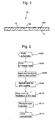
- a method for manufacturing an optical recording medium 10 shown in Fig. 1 has a feature.
- first the structure of the optical recording medium 10 is briefly described.
- the optical recording medium 10 includes a substrate 12 having a surface serving as an information recording surface 12A, and a light transmitting layer 14 that is formed on the information recording surface 12A to be thinner than the substrate 12.
- the optical recording medium 10 is a circular disk having an outer diameter of approximately 120 mm and a thickness of approximately 1.2 mm, and has a central hole 10A having an inner diameter of approximately 15 mm.
- the substrate 12 is formed of a resin such as polycarbonate, acrylic resin, epoxy resin, and has a thickness of approximately 1.1 mm.
- fine concave and convex portions (not shown) for carrying information, such as pits and grooves.
- pits and grooves are generally used to mean concave portions for carrying information, those terms are used herein to mean not only the concave portions but also convex portions for carrying information for convenience.
- a functional layer is formed on the information recording surface 12A.
- the functional layer is thinner than the light transmitting layer 14 and appears to be needless to understand the present invention, the functional layer is not shown in the drawings.
- the optical recording medium 10 is a ROM (Read Only Memory) type disc
- a reflection layer of Al, Ag, Au or the like is formed as the functional layer on the information recording surface 12A.
- RW Re-Writable
- a recording layer made of a phase change material, a magneto-optical material or the like is formed in addition to the reflection layer.
- an R (Recordable) type disc a recording layer made of phase change material or including organic dye is formed in addition to the reflection layer.
- the light transmitting layer 14 is formed on the functional layer and has a thickness of approximately 0.1 mm.
- the light transmitting layer 14 is formed of a material that can be cured by radiation and can transmit light, for example, acrylic UV curable resin or epoxy UV curable resin.
- a manufacturing hole 12B for use in manufacturing having a smaller inner diameter than that of the aforementioned central hole 10A is formed in the substrate 12.
- the manufacturing hole 12B have an inner diameter of 10 mm or less.
- the inner diameter of the manufacturing hole 12B is preferably 3 mm or more, considering the molding of the substrate 12 by injection molding, for example.
- fine concave and convex portions for carrying information are transferred onto the information recording surface 12A that is one surface of the substrate 12.
- a circular concave portion 12C having an inner diameter which is equal to that of the central hole 10A is formed.
- a plurality of substrates 12 are usually stored or transferred while being stacked. For example, by inserting a guide in the form of a round bar or the like, into the manufacturing hole 12B, it is easy to stack a plurality of substrates 12 while they are aligned. This makes the storage or transfer of the substrates easier, thus improving production efficiency.
- a functional layer (not shown) is formed by sputtering, deposition, or the like (Step S104).
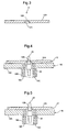
- the rotating table 18 has a structure in which a shaft 18B projects downward from a table part 18A in the form of a circular disk placed horizontally. Within the shaft 18B, a vent hole 18C is formed to be in communication with the table part 18A. The shaft 18B is engaged with a rotating driving mechanism that is not shown. Moreover, to the vent hole 18C, a negative-pressure supply that is not shown is connected.
- the core member 20 is formed of a silicone resin, a fluororesin, an acrylic resin, an olefin resin, or a mixture of them, and has elasticity.
- the core member 20 is a round bar having an outer diameter slightly smaller than the inner diameter of the manufacturing hole 12B in its original state, and can be fitted into the manufacturing hole 12B freely.
- the core member 20 is supported by a compression/release mechanism 21 at a portion near its lower end, and is configured in such a manner that the outer diameter is increased when the compression/release mechanism 21 compresses the core member 20 in an axial direction, thereby the core member 20 comes into close contact with the inner circumference of the manufacturing hole 12B.
- the core member 20 is compressed in the axial direction by the compression/release mechanism 21 so as to come into close contact with the inner circumference of the manufacturing hole 12B (Step S106). Then, a negative pressure is supplied to an upper surface of the table part 18A so as to absorb the substrate 12 and fix it onto the rotating table 18.
- a nozzle 22 is brought close to a region surrounding the core member 20 and a predetermined amount of radiation curable resin, that is fluid, is supplied onto the substrate 12 from the nozzle 22.
- the radiation curable resin does not enter a gap between the core member 20 and the substrate 12 because the core member 20 is in close contact with the manufacturing hole 12B.
- the radiation curable resin thus supplied is spread outward in a radial direction by centrifugal force.
- centrifugal force hardly acts on the resin in the vicinity of the manufacturing hole 12B having a smaller inner diameter than that of the central hole 10A. Therefore, the region in the vicinity of the manufacturing hole 12B serves as reservoir of resin, and buffers and stabilizes the amount of the flowing resin on the information recording surface 12A.
- the light transmitting layer 14 is spread over the information recording surface 12A with a uniform thickness of approximately 0.1 mm (Step S108).
- Step S110 the rotation of the rotating table 18 is stopped, and the light transmitting layer 14 thus spread is uniformly irradiated with UV rays, so that the light transmitting layer 14 is cured.
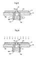
- Step S112 the substrate 12 is removed from the rotating table 18 and the core member 20. Since the core member 20 is formed of rubber or the like, it is hard to adhere to the light transmitting layer 14. Therefore, it is possible to easily remove the substrate 12 from the core member 20.
- a jig 22 is fitted into the manufacturing hole 12B so as to position the substrate 12.
- a circular tool 24 having an outer diameter equal to the inner diameter of the central hole 10A is arranged concentrically with respect to the substrate 12, and is brought into contact with the substrate 12 in the axial direction and is penetrated through the substrate 12 so as to punch out a hole in the substrate 12.
- the central hole 10A is formed (Step S114). Since the substrate 12 has the circular concave portion 12C having the inner diameter equal to that of the central hole 10A, the punching of the central hole can be easily done.
- the core member 20 is a round bar that has elasticity and has an outer diameter slightly smaller than the inner diameter of the manufacturing hole 12B in its original state, and can be freely fitted into the manufacturing hole 12B.
- the core member can come into close contact with the inner circumference of the manufacturing hole 12B, there is no restriction to the material and shape of the core member.
- the substrate is formed by injection molding, which includes the circular concave portion 12C having the same inner diameter as that of the central hole (that has the inner diameter larger than that of the manufacturing hole 12B), in the opposite surface to the information recording surface 12A.
- the substrate 12 in which the opposite surface to the information recording surface 12A is flat may be formed by injection molding.
- acrylic UV curable resin and epoxy UV curable resin are described as examples of the material for the light transmitting layer 14.
- a thermosetting resin, a two-component curing resin or other types of radiation curable resin that can be cured by other types of radiation, such as an electron beam can be used as the material for the light transmitting layer 14, as long as it can transmit light.
- the optical recording medium 10 is a single-sided type in which information can be recorded on one surface only.
- the exemplary embodiment of the present invention can also be applied to a double-sided optical recording medium in which information can be recorded on both surfaces.
- the optical recording medium having a total thickness of 1.2 mm can be obtained.
- ten substrates 12 were molded for each of respective 10 inner diameters of the manufacturing hole 12B, i.e., 2 mm, 4 mm, 5 mm, 6 mm, 7 mm, 8 mm, 9 mm, 10 mm, 12 mm and 14 mm, so that a total of 100 substrates 12 were molded.
- a resin was spread on the information recording surface 12A of the substrate 12 under a condition of spin-coating in which revolutions per minute of the turntable 18 was approximately 2000 rpm. Then, the resin was exposed to UV rays, thereby being cured to form a light transmitting layer 14. In this manner, 100 optical recording media 10 were fabricated. In this manufacturing, the following materials were used for the light transmitting layer 14.
- ARONIX® M-315 (manufactured by Toagosei Co., Ltd.): 10 wt%
- THF-A (manufactured by Kyoeisha Chemical Co., Ltd.): 10 wt%
- Irgacure® 184 (manufactured by Ciba Specialty Chemicals K. K.): 3 wt%
- Viscosity of the resin before curing 6800 mPa ⁇ s
- the thickness of the light transmitting layer 14 was measured at 1140 points in a region of 22-58 mm from the center with approximately 2 mm intervals in the radial direction and with approximately 6 degrees intervals in the circumferential direction by means of a thickness measuring device Core 9930a (manufactured by cores Co., Ltd.).
- Table 1 shows an average of the thickness of the light transmitting layers 14 on the respective optical recording media 10 and a difference between the minimum thickness and the maximum thickness thereof, for each inner diameter of the manufacturing hole 12B.
- the average and difference of the thickness in Table 1 are averaged values of ten optical recording media 10 having the manufacturing holes 12B of the same inner diameter.
- the optical recording media 10 in which the light transmitting layers 14 looked good are shown with "o" for the respective inner diameters of the manufacturing hole 12B in Table 1. Please not that "o” represents that the light transmitting layer 14 looked good for all the ten optical recording media 10 having the manufacturing holes 12B of the same inner diameter.
- a time required for spin-coating was longer as the inner diameter of the manufacturing hole 12B was smaller. That is, the time required for spin-coating was varied depending on the inner diameter of the manufacturing hole 12B. Thus, that time is shown for each inner diameter in Table 1 for reference.
- the light transmitting layers 14 had good appearance.
- Inner diameter of manufacturing hole (mm) Average of thickness of light transmitting layer ( ⁇ m) Difference of thickness of light transmitting layer ( ⁇ m) Time required for spin-coating (SEC) Appearance of light transmitting layer 2 99.9 0.71 10.5 ⁇ 4 99.9 0.71 10.5 ⁇ 5 99.9 0.71 10.5 ⁇ 6 100.1 1.82 10.3 ⁇ 7 100.0 1.99 10.3 ⁇ 8 99.6 2.55 10.3 ⁇ 9 100.7 3.20 10.0 ⁇ 10 100.3 3.84 10.0 ⁇ 12 99.8 4.53 10.0 ⁇ 14 100.0 6.61 9.7 ⁇
- 100 optical recording media 10 were fabricated under the same condition as that of the above example except for the following points. While the core member 20 was not brought into close contact with the inner circumference of the manufacturing hole 12B and therefore there was a gap between the inner circumference of the manufacturing hole 12B and the core member 20, the resin was spread on the information recording surface 12A of the substrate 12. Then, the resin was cured by being exposed to UV rays, thereby forming the light transmitting layer 14. For each of the thus fabricated 100 optical recording media 10, the thickness of the light transmitting layer 14 was measured. In addition, for each of the 100 optical recording media 10, the appearance of the light transmitting layer 14 was also visually checked.
- Table 2 shows, for each of the inner diameters of the manufacturing hole 12B, the average of the thickness of the light transmitting layers 14 on the respective optical recording media 10 and the difference between the minimum thickness and the maximum thickness thereof.
- the optical recording media 10 having the light transmitting layers 14 that looked good are shown with "o”
- the optical recording media 10 having the light transmitting layers 14 that did not look good are shown with " ⁇ " in table 2.
- the difference of the thickness of the light transmitting layer 14 tended to be smaller in a case where the core member 20 was in close contact with the inner circumference of the manufacturing hole 12B (Example) than in a case where the core member 20 was not in close contact with the inner circumference of the manufacturing hole 12B (Comparative Example).
- the various exemplary embodiments of the present invention can be used for forming a light transmitting layer, that is thinner than a substrate of an optical recording medium, to have a uniform thickness.
Landscapes
- Engineering & Computer Science (AREA)
- Mechanical Engineering (AREA)
- Manufacturing & Machinery (AREA)
- Manufacturing Optical Record Carriers (AREA)
- Optical Record Carriers And Manufacture Thereof (AREA)
Applications Claiming Priority (2)
| Application Number | Priority Date | Filing Date | Title |
|---|---|---|---|
| JP2003312779A JP2005085302A (ja) | 2003-09-04 | 2003-09-04 | 光記録媒体の製造方法 |
| JP2003312779 | 2003-09-04 |
Publications (2)
| Publication Number | Publication Date |
|---|---|
| EP1512522A2 true EP1512522A2 (de) | 2005-03-09 |
| EP1512522A3 EP1512522A3 (de) | 2005-06-15 |
Family
ID=34131869
Family Applications (1)
| Application Number | Title | Priority Date | Filing Date |
|---|---|---|---|
| EP04021032A Withdrawn EP1512522A3 (de) | 2003-09-04 | 2004-09-03 | Verfahren zur Herstellung von einem optischen Informationsträger |
Country Status (3)
| Country | Link |
|---|---|
| US (1) | US20050053750A1 (de) |
| EP (1) | EP1512522A3 (de) |
| JP (1) | JP2005085302A (de) |
Families Citing this family (1)
| Publication number | Priority date | Publication date | Assignee | Title |
|---|---|---|---|---|
| CN110775981B (zh) * | 2019-11-26 | 2023-11-17 | 青岛大学 | 二氧化硅微球及其制造方法 |
Family Cites Families (3)
| Publication number | Priority date | Publication date | Assignee | Title |
|---|---|---|---|---|
| JP2001006210A (ja) * | 1999-06-22 | 2001-01-12 | Sony Corp | 光記録媒体及びディスクカートリッジ |
| JP2003067991A (ja) * | 2001-06-07 | 2003-03-07 | Fuji Photo Film Co Ltd | 光ディスクの製造方法及びディスク積層体の搬送方法 |
| JP3662531B2 (ja) * | 2001-09-11 | 2005-06-22 | Tdk株式会社 | 光ディスクの製造方法および装置 |
-
2003
- 2003-09-04 JP JP2003312779A patent/JP2005085302A/ja not_active Withdrawn
-
2004
- 2004-08-31 US US10/929,681 patent/US20050053750A1/en not_active Abandoned
- 2004-09-03 EP EP04021032A patent/EP1512522A3/de not_active Withdrawn
Also Published As
| Publication number | Publication date |
|---|---|
| EP1512522A3 (de) | 2005-06-15 |
| JP2005085302A (ja) | 2005-03-31 |
| US20050053750A1 (en) | 2005-03-10 |
Similar Documents
| Publication | Publication Date | Title |
|---|---|---|
| US6404730B2 (en) | Optical disk having a groove and a projection for combining two disk members | |
| KR100952067B1 (ko) | 광학 기록매체 | |
| CN100454416C (zh) | 光信息记录介质的制造方法 | |
| US20030137922A1 (en) | Method of manufacturing optical disk | |
| JP2002170279A (ja) | 光学記録媒体およびその製造方法、ならびに射出成形装置 | |
| JP2002063737A (ja) | 光情報媒体およびその製造方法 | |
| US20050072518A1 (en) | Method of manufacturing disc-shaped recording medium | |
| EP1512522A2 (de) | Verfahren zur Herstellung von einem optischen Informationsträger | |
| US7680018B2 (en) | Optical recording medium, and manufacturing method and manufacturing device thereof | |
| EP1515325A2 (de) | Verfahren zum Herstellen eines optischen Vielschicht-Aufzeichnungsmediums und eines Zwischenprodukts im Herstellungsverfahren desselben | |
| US7502309B2 (en) | Optical recording medium having a relationship between convex width and track pitch | |
| US20050093185A1 (en) | Method of manufacturing optical recording medium | |
| EP1756819B1 (de) | Vorrichtung zum anbringen und ablösen einer kappe für eine aufschleuderbeschichtung eines optischen datenträgers, vorrichtung für die aufschleuderbeschichtung eines optischen datenträgers damit, verfahren zur herstellung eines optischen datenträgers unter verwendung der vorrichtung zum anbringen und ablösen einer kappe für die aufschleuderbeschichtung eines optischen datenträgers | |
| US20050226131A1 (en) | Optical recording medium, and manufacturing method and manufacturing device thereof | |
| KR100922428B1 (ko) | 광디스크 스핀코팅용 장치 및 이를 이용한 광디스크제조방법 | |
| KR100859797B1 (ko) | 광디스크 스핀코팅용 장치 | |
| JP4561539B2 (ja) | 光記録媒体の製造方法、製造装置及び光記録媒体 | |
| KR100733919B1 (ko) | 광디스크의 제조방법 | |
| US20050084644A1 (en) | Optical recording medium and method for fabricating the same | |
| JP2007073124A (ja) | 光記録媒体の製造方法及び製造装置 | |
| JP2010244625A (ja) | 多層型光情報記録媒体 | |
| JP2003257091A (ja) | 光ディスク基板の製造方法 |
Legal Events
| Date | Code | Title | Description |
|---|---|---|---|
| PUAI | Public reference made under article 153(3) epc to a published international application that has entered the european phase |
Free format text: ORIGINAL CODE: 0009012 |
|
| AK | Designated contracting states |
Kind code of ref document: A2 Designated state(s): AT BE BG CH CY CZ DE DK EE ES FI FR GB GR HU IE IT LI LU MC NL PL PT RO SE SI SK TR |
|
| AX | Request for extension of the european patent |
Extension state: AL HR LT LV MK |
|
| PUAL | Search report despatched |
Free format text: ORIGINAL CODE: 0009013 |
|
| AK | Designated contracting states |
Kind code of ref document: A3 Designated state(s): AT BE BG CH CY CZ DE DK EE ES FI FR GB GR HU IE IT LI LU MC NL PL PT RO SE SI SK TR |
|
| AX | Request for extension of the european patent |
Extension state: AL HR LT LV MK |
|
| AKX | Designation fees paid | ||
| 17P | Request for examination filed |
Effective date: 20051214 |
|
| RBV | Designated contracting states (corrected) |
Designated state(s): AT BE BG CH CY CZ DE DK EE ES FI FR GB GR HU IE IT LI LU MC NL PL PT RO SE SI SK TR |
|
| 17Q | First examination report despatched |
Effective date: 20060808 |
|
| STAA | Information on the status of an ep patent application or granted ep patent |
Free format text: STATUS: THE APPLICATION IS DEEMED TO BE WITHDRAWN |
|
| 18D | Application deemed to be withdrawn |
Effective date: 20090331 |