EP1511148A2 - Überspannungs-Unterdrücker - Google Patents
Überspannungs-Unterdrücker Download PDFInfo
- Publication number
- EP1511148A2 EP1511148A2 EP04254876A EP04254876A EP1511148A2 EP 1511148 A2 EP1511148 A2 EP 1511148A2 EP 04254876 A EP04254876 A EP 04254876A EP 04254876 A EP04254876 A EP 04254876A EP 1511148 A2 EP1511148 A2 EP 1511148A2
- Authority
- EP
- European Patent Office
- Prior art keywords
- voltages
- surge
- motor
- ground
- phases
- Prior art date
- Legal status (The legal status is an assumption and is not a legal conclusion. Google has not performed a legal analysis and makes no representation as to the accuracy of the status listed.)
- Withdrawn
Links
Images

Classifications
-
- H—ELECTRICITY
- H02—GENERATION; CONVERSION OR DISTRIBUTION OF ELECTRIC POWER
- H02H—EMERGENCY PROTECTIVE CIRCUIT ARRANGEMENTS
- H02H7/00—Emergency protective circuit arrangements specially adapted for specific types of electric machines or apparatus or for sectionalised protection of cable or line systems, and effecting automatic switching in the event of an undesired change from normal working conditions
- H02H7/08—Emergency protective circuit arrangements specially adapted for specific types of electric machines or apparatus or for sectionalised protection of cable or line systems, and effecting automatic switching in the event of an undesired change from normal working conditions for dynamo-electric motors
- H02H7/0833—Emergency protective circuit arrangements specially adapted for specific types of electric machines or apparatus or for sectionalised protection of cable or line systems, and effecting automatic switching in the event of an undesired change from normal working conditions for dynamo-electric motors for electric motors with control arrangements
- H02H7/0838—Emergency protective circuit arrangements specially adapted for specific types of electric machines or apparatus or for sectionalised protection of cable or line systems, and effecting automatic switching in the event of an undesired change from normal working conditions for dynamo-electric motors for electric motors with control arrangements with H-bridge circuit
-
- H—ELECTRICITY
- H02—GENERATION; CONVERSION OR DISTRIBUTION OF ELECTRIC POWER
- H02H—EMERGENCY PROTECTIVE CIRCUIT ARRANGEMENTS
- H02H9/00—Emergency protective circuit arrangements for limiting excess current or voltage without disconnection
- H02H9/04—Emergency protective circuit arrangements for limiting excess current or voltage without disconnection responsive to excess voltage
- H02H9/042—Emergency protective circuit arrangements for limiting excess current or voltage without disconnection responsive to excess voltage comprising means to limit the absorbed power or indicate damaged over-voltage protection device
Definitions
- the present invention relates to a surge voltage suppressor for suppressing surge voltages that are generated in a motor when the motor is PWM-controlled by means of an inverter.
- DC voltage is converted into AC voltage by switching power transistors or other switching elements for PWM control, and the AC voltage is applied to windings for the individual phases of the motor.
- the DC voltage is on-off controlled with the switching elements. If power lines for connection with the motor are long, their inductance increases so that surge voltages are generated between three-phase windings in the motor and between the ground and the windings. These surge voltages inevitably lower the effect of insulation between the windings and between the ground and the windings.
- a filter that is composed of a reactor and a capacitor is provided between the inverter and the motor to remove the surge voltages.
- a three-phase diode bridge is connected to power lines for three-phase windings of a motor.
- a capacitor and a resistor are connected in parallel with the output of the diode bridge, and the capacitor is charged to a maximum output voltage of the inverter. If surge voltages are generated, the capacitor absorbs their energy through the diode bridge. The absorbed energy is consumed by the resistor that is connected in parallel with the capacitor or a reactor that is connected to positive and negative DC current bus terminals of the inverter.
- a surge voltage suppressor for suppressing surge voltages generated in a motor driven by a PWM control inverter.
- semiconductor surge absorbing devices adapted to be energized to clamp voltages when the voltages are higher than a given value are connected to power lines of the motor, whereby the surge voltages between the phases of the motor and between the ground and the phases are suppressed.
- the surge voltage suppressor is constructed so that the semiconductor surge absorbing devices are connected individually between the phases of the power lines of the motor and between the ground and the phases.
- the suppressor is designed so that the semiconductor surge absorbing devices are connected individually between the phases of the power lines of the motor or between the ground and the phases.
- the suppressor is constructed so that on terminal of each of the semiconductor surge absorbing devices is connected to one of the power lines for the individual phases of the motor, while the other terminal is connected to one terminal of a semiconductor surge absorbing device of which the other terminal is connected to the ground.
- the surge voltage suppressor is constructed so that the individual phases of the power lines of the motor are connected to a three-phase full-wave rectifier, and that the semiconductor surge absorbing devices are connected individually between a positive terminal and a negative terminal of the full-wave rectifier, between the positive terminal and the ground, and between the negative terminal and the ground.
- the surge voltage suppressor is designed so that the individual phases of the power lines of the motor are connected to a three-phase full-wave rectifier, and that the semiconductor surge absorbing devices are connected between a positive terminal and a negative terminal of the full-wave rectifier, or connected individually between the positive terminal and the ground and between the negative terminal and the ground.
- the semiconductor surge absorbing devices are mounted on a printed board housed in a hermetically sealed case. Thus, cutting oil or chips are prevented from adhering to the devices or the printed board. Furthermore, the case is used doubling as a terminal box attached to the motor.
- a compact surge voltage suppressor that can absorb only surge energy without wasting energy.
- surge energy can be securely absorbed with use of a simple construction that requires only a narrow setting space, and the effect of insulation between the phases of the motor and between the ground and the phases can be prevented from lowering.
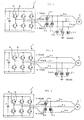
- FIG. 1 is a block diagram showing principal parts according to a first embodiment of the invention.
- Numeral 1 denotes a conventional inverter that converts DC voltage into AC voltage by PWM control.
- Parallel-connected sets of switching elements Q such as power transistors, and diodes D are connected in series between positive and negative terminals of a DC power supply for the U, V and W phases.
- Outputs from the inverter 1 for the individual phases are fetched from series-connection nodes of the parallel-connected sets of switching elements Q and diodes D, and delivered to U-, V- and W-phase windings of a motor 2 by means of power lines 4u, 4v and 4w, individually.
- Symbol C in the inverter 1 designates a capacitor of the DC power supply.
- Semiconductor surge absorbing devises 3 are connected between the phases and between the ground and the phases. They have characteristics such that current flows through them to clamp voltage when the voltage reaches a given or higher value. More specifically, the semiconductor surge absorbing devises 3a, 3b and 3c are connected between the U- and V-phase power lines 4u and 4v, between the V- and W-phase power lines 4v and 4w, and between the U- and W-phase power lines 4u and 4w, respectively.
- the semiconductor surge absorbing devises 3d, 3e and 3f are connected between the ground and the U-, V- and W-phase power lines 4u, 4v and 4w, respectively.
- the semiconductor surge absorbing devises 3 are arranged so that a plurality of semiconductor surge absorbing device elements are connected in series to obtain a desired clamping voltage. If the withstand voltage of the motor is 1,000 V, for example, the semiconductor surge absorbing device elements can be connected in series to adjust the clamping voltage to less than 1,000 V, e.g., to 700 V.
- the switching elements Q are switched on to actuate the motor 2 in response to a PWM signal. If voltage across each semiconductor surge absorbing device 3 is increased to a preset clamping voltage or higher due to surge voltages that are generated by this switching operation, the device 3 is energized to cause current flow, and the voltage of the power line 4 is clamped to a preset desired value. Thereupon, the surge voltages are absorbed.
- a clamping voltage e.g. 700 V
- the device 3a is energized to cause current flow, so that the voltage between the power lines 4u and 4v never exceeds the clamping voltage.
- deterioration in insulation between the U- and V-phase power lines 4u and 4v can be prevented.
- the devices 3b and 3c are energized to cause current flow, thereby absorbing the surge voltages. If voltages between the ground and the individual phases exceed clamping voltages that are set in the semiconductor surge absorbing devices 3d, 3e and 3f, moreover, the devices 3d, 3e and 3f are energized to cause current flow, thereby absorbing the surge voltages. Thus, deterioration in insulation between the phases and between the ground and the phases by the surge voltages can be prevented.
- the semiconductor surge absorbing devices 3 (3a to 3f) consume only surge energy that is produced by the voltages between the terminals of respective devices 3 when the switching elements Q are switched on, so that energy can be consumed efficiently without waste.
- FIG. 2 is a block diagram showing principal parts according to a second embodiment of the invention.
- the semiconductor surge absorbing devices 3a, 3b and 3c between the power lines 4u, 4v and 4w for the individual phases according to the first embodiment shown in FIG. 1 are omitted, and semiconductor surge absorbing devices 3d, 3e and 3f are arranged only between the ground and the power lines 4u, 4v and 4w. If voltages between the ground and the power lines 4u, 4v and 4w exceed the clamping voltages of the semiconductor surge absorbing devices 3d, 3e and 3f, the devices 3d, 3e and 3f are energized and absorb the surge voltages.
- FIG. 3 is a block diagram showing principal parts according to a third embodiment of the invention.
- the semiconductor surge absorbing devices 3d, 3e and 3f between the ground and the power lines 4u, 4v and 4w for the individual phases according to the first embodiment shown in FIG. 1 are omitted, and semiconductor surge absorbing devices 3a, 3b and 3c are arranged only between the power lines 4u, 4v and 4w. If voltages between the phases are increased above the' clamping voltages, the semiconductor surge absorbing devices 3a, 3b and 3c are energized and absorb the surge voltages.
- the first to third embodiments may be used alternatively, depending on the specifications and characteristics of the motor and the like.
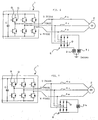
- FIG. 4 is a block diagram showing principal parts according to a fourth embodiment of the invention.
- the semiconductor surge absorbing devices 3 are reduced in number to achieve the same functions of the first embodiment shown in FIG. 1.
- one terminal of each of the semiconductor surge absorbing devices 3d, 3e and 3f is connected to one of the power lines 4u, 4v and 4w for the individual phases of the motor that connect outputs for the phases of the inverter 1 and windings for the phases.
- the other terminal of each of the devices 3d, 3e and 3f is connected to one terminal of a semiconductor surge absorbing device 3g.
- the other terminal of the device 3g is connected to the ground.
- the U-phase power line 4u is connected to the ground through a series circuit of two semiconductor surge absorbing devices 3d and 3g.
- the V-phase power line 4v is connected to the ground through a series circuit of two devices 3e and 3g, and the W-phase power line 4w to the ground through a series circuit of two devices 3f and 3g.
- the U- and V-phase power lines 4u and 4v are connected to each other through the semiconductor surge absorbing devices 3d and 3e.
- the V- and W-phase power lines 4v and 4w are connected to each other through the devices 3e and 3f, and the U- and W-phase power lines 4u and 4w through the devices 3d and 3f.
- the same functions of the first embodiment can be achieved by adjusting the clamping voltages of the semiconductor surge absorbing devices 3d to 3g to 350 V.
- the U and V phases are connected through the devices 3d and 3e, so that the clamping voltages are adjusted to 700 V.
- the V and W phases and the U and W phases are connected through the devices 3e and 3f and the devices 3d and 3f, respectively, so that the voltages between these phases are clamped to 700 V.
- the power lines 4u, 4v and 4w for the individual phases are connected to the ground through the semiconductor surge absorbing devices 3d, 3e and 3f, respectively, and the semiconductor surge absorbing device 3g. Therefore, the voltages between the ground and the phases are also clamped to 700 V, and the surge voltages are absorbed through the devices 3d to 3g.
- the semiconductor surge absorbing devices 3 used in the first embodiment shown in FIG. 1 are six in number, those used in the fourth embodiment shown in FIG. 4 are four. Further, the respective clamping voltages of the devices 3d to 3g of the fourth embodiment are only half those of the devices 3 of the first embodiment shown in FIG. 1. Therefore, the semiconductor surge absorbing device elements that constitute the semiconductor surge absorbing devices 3 can be reduced in number. Thus, the device elements are so few, as a whole, that the resulting structure can be low-priced.
- FIG. 5 is a block diagram showing principal parts according to a fifth embodiment of the invention.
- a three-phase full-wave rectifier 5 is used to detect voltages and absorb the surge voltages.
- Input terminals of the three-phase full-wave rectifier 5 are connected individually to the U-, V-and W-phase power lines, while its output terminals are connected to each other by means of a semiconductor surge absorbing device 3h.
- the positive output terminal of the rectifier 5 is connected to the ground through a semiconductor surge absorbing device 3j.
- the negative output terminal of the rectifier 5 is connected to the ground through a semiconductor surge absorbing device 3i.
- Symbol D in the three-phase full-wave rectifier 5 denotes the diodes that constitute the rectifier 5.
- the device 3h If a surge voltage causes a voltage between phases to exceed the clamping voltage of the semiconductor surge absorbing device 3h, the device 3h is energized and absorbs the surge voltages. If a positive surge voltage is generated against the ground and exceeds the clamping voltage of the semiconductor surge absorbing device 3j, the device 3j is energized and absorbs the surge voltage. Likewise, if a negative surge voltage is generated against the ground and exceeds the clamping voltage of the semiconductor surge absorbing device 3i, the device 3i is energized and absorbs the surge voltage.
- FIG. 6 shows a sixth embodiment of the invention.
- the semiconductor surge absorbing device 3h that is connected between the output terminals of the three-phase full-wave rectifier 5 of the fifth embodiment shown in FIG. 5 and clamps the phase voltage is omitted.
- the sixth embodiment shares other configurations and functions with the fifth embodiment.
- FIG. 7 shows a seventh embodiment of the invention.
- the semiconductor surge absorbing devices 3i and 3j between the ground and the output terminals of the three-phase full-wave rectifier 5 of the fifth embodiment shown in FIG. 5 is omitted.
- the seventh embodiment shares a function with the semiconductor surge absorbing device 3h between the output terminals of the three-phase full-wave rectifier 5 described in connection with the fifth embodiment.
- the fifth to seventh embodiments may be also used alternatively, depending on the specifications or the like of the motor.
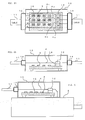
- FIGS. 8A and 8B are views illustrating an example of the way the semiconductor surge absorbing devices 3 according to the above-described embodiments are mounted.
- FIG. 8A is a plan view showing a case 13 with its top plate off.
- FIG. 8B is a side view showing the case 13 with its side plate off.
- the semiconductor surge absorbing devices are mounted on a printed board 10, which is housed in the hermetically sealed case 13.
- a cable 11 for the power lines are attached to the case 13 by means of a connector 14.
- the U-, V- and W-phase power lines 4u, 4v and 4w and a ground wire 4g are led out of the connector 14, and are fixed to the printed board 10 by means of screws 12 on the board 10 to be connected electrically to the devices 3.
- the case 13 is formed having a hermetically sealed structure for the following reason.
- the inverter and the motor, which are used to drive a machine tool or the like, are located in a tough environment. Therefore, cutting oil, chips that are produced by machining operation of the machine tool, and the like must be prevented from adhering to the printed board 10, semiconductor surge absorbing devices 3, etc. If the working environment is favorable, however, the case need not be hermetically sealed.
- FIG. 9 shows another example in which the case 13 that houses the printed board 10 on which the semiconductor surge absorbing devices 3 are mounted is used doubling as a terminal box that is attached to the motor 2.
- the motor 2 is provided with the terminal box that houses terminals for connecting the windings of the motor and the power lines 4u, 4v and 4w.
- This terminal box serves also as the case 13 that houses the printed board 10 on which the devices 3 are mounted.
Landscapes
- Inverter Devices (AREA)
- Emergency Protection Circuit Devices (AREA)
- Power Conversion In General (AREA)
Applications Claiming Priority (2)
| Application Number | Priority Date | Filing Date | Title |
|---|---|---|---|
| JP2003302477A JP3742636B2 (ja) | 2003-08-27 | 2003-08-27 | サージ電圧抑制装置 |
| JP2003302477 | 2003-08-27 |
Publications (1)
| Publication Number | Publication Date |
|---|---|
| EP1511148A2 true EP1511148A2 (de) | 2005-03-02 |
Family
ID=34101188
Family Applications (1)
| Application Number | Title | Priority Date | Filing Date |
|---|---|---|---|
| EP04254876A Withdrawn EP1511148A2 (de) | 2003-08-27 | 2004-08-13 | Überspannungs-Unterdrücker |
Country Status (4)
| Country | Link |
|---|---|
| US (1) | US20050047050A1 (de) |
| EP (1) | EP1511148A2 (de) |
| JP (1) | JP3742636B2 (de) |
| CN (1) | CN1592068A (de) |
Cited By (2)
| Publication number | Priority date | Publication date | Assignee | Title |
|---|---|---|---|---|
| WO2007039369A1 (de) * | 2005-09-30 | 2007-04-12 | Siemens Aktiengesellschaft | Ansteuersystem und verfahren zur ansteuerung für einen permanent erregten elektromotor |
| CN104467384A (zh) * | 2013-09-17 | 2015-03-25 | 北京计算机技术及应用研究所 | 一种变频器尖峰电压吸收装置、方法及系统 |
Families Citing this family (7)
| Publication number | Priority date | Publication date | Assignee | Title |
|---|---|---|---|---|
| CN102027661B (zh) * | 2008-05-14 | 2015-04-22 | 大金工业株式会社 | 滤波电路安装单元及电源单元 |
| JP5272593B2 (ja) * | 2008-09-02 | 2013-08-28 | トヨタ自動車株式会社 | 電動機駆動システムおよびそれを備えた車両 |
| JP5452155B2 (ja) * | 2009-10-06 | 2014-03-26 | 東芝シュネデール・インバータ株式会社 | サージ電圧抑制装置およびモータ制御装置 |
| JP5537113B2 (ja) * | 2009-10-06 | 2014-07-02 | 東芝シュネデール・インバータ株式会社 | サージ電圧確認方法 |
| JP5574771B2 (ja) * | 2010-03-18 | 2014-08-20 | 株式会社日本自動車部品総合研究所 | 電動機制御装置、および、これを用いた電動機システム |
| US10516332B2 (en) * | 2016-08-09 | 2019-12-24 | Hitachi Automotive Systems, Ltd. | Induced voltage suppression device, motor system, and power conversion system |
| CN110112721B (zh) * | 2019-05-23 | 2022-04-15 | 清华大学 | 一种直流配电网系统内部过电压防护系统与方法 |
Family Cites Families (17)
| Publication number | Priority date | Publication date | Assignee | Title |
|---|---|---|---|---|
| US3693053A (en) * | 1971-10-29 | 1972-09-19 | Gen Electric | Metal oxide varistor polyphase transient voltage suppression |
| US3894274A (en) * | 1974-07-01 | 1975-07-08 | Gen Electric | Electric motor transient voltage suppressing circuit |
| US4023071A (en) * | 1975-06-09 | 1977-05-10 | Fussell Gerald W | Transient and surge protection apparatus |
| US4271446A (en) * | 1977-06-27 | 1981-06-02 | Comstock Wilford K | Transient voltage suppression system |
| US4419711A (en) * | 1979-12-28 | 1983-12-06 | Seguin Herb J J | Method and apparatus for the protection of electrical equipment from high voltage transients |
| JP3142617B2 (ja) * | 1991-11-27 | 2001-03-07 | 新電元工業株式会社 | サージ防護素子 |
| US5412526A (en) * | 1993-02-10 | 1995-05-02 | Square D Company | Surge arrester circuit and housing therefor |
| US5483086A (en) * | 1993-04-20 | 1996-01-09 | Shindengen Electric Manufacturing Co., Ltd. | Four layer semiconductor surge protector having plural short-circuited junctions |
| US5661390A (en) * | 1995-06-23 | 1997-08-26 | Electric Power Research Institute, Inc. | Inverter-fed motor drive with EMI suppression |
| US5646498A (en) * | 1995-08-07 | 1997-07-08 | Eaton Corporation | Conducted emission radiation suppression in inverter drives |
| US5757603A (en) * | 1996-06-21 | 1998-05-26 | Joslyn Electronic Systems Corporation | Electrical surge protection device |
| US6118639A (en) * | 1997-05-30 | 2000-09-12 | Goldstein; Richard | Fast acting disconnect system for protecting surge suppressors and connected utilization equipment from power line overvoltages |
| US5986870A (en) * | 1997-09-16 | 1999-11-16 | Joselyn Electronics Systems Company | Electrical surge protector with protective enclosure |
| US6069781A (en) * | 1998-06-17 | 2000-05-30 | Maxi Volt Corporation, Inc. | Device for protecting medium voltage equipment against voltage surges |
| JP3955396B2 (ja) * | 1998-09-17 | 2007-08-08 | 株式会社ルネサステクノロジ | 半導体サージ吸収素子 |
| US6615147B1 (en) * | 1999-08-09 | 2003-09-02 | Power Measurement Ltd. | Revenue meter with power quality features |
| US6477025B1 (en) * | 1999-10-12 | 2002-11-05 | Innovative Technology, Inc. | Surge protection device with thermal protection, current limiting, and failure indication |
-
2003
- 2003-08-27 JP JP2003302477A patent/JP3742636B2/ja not_active Expired - Fee Related
-
2004
- 2004-08-12 US US10/916,487 patent/US20050047050A1/en not_active Abandoned
- 2004-08-13 EP EP04254876A patent/EP1511148A2/de not_active Withdrawn
- 2004-08-17 CN CNA2004100582121A patent/CN1592068A/zh active Pending
Cited By (2)
| Publication number | Priority date | Publication date | Assignee | Title |
|---|---|---|---|---|
| WO2007039369A1 (de) * | 2005-09-30 | 2007-04-12 | Siemens Aktiengesellschaft | Ansteuersystem und verfahren zur ansteuerung für einen permanent erregten elektromotor |
| CN104467384A (zh) * | 2013-09-17 | 2015-03-25 | 北京计算机技术及应用研究所 | 一种变频器尖峰电压吸收装置、方法及系统 |
Also Published As
| Publication number | Publication date |
|---|---|
| JP3742636B2 (ja) | 2006-02-08 |
| JP2005073439A (ja) | 2005-03-17 |
| US20050047050A1 (en) | 2005-03-03 |
| CN1592068A (zh) | 2005-03-09 |
Similar Documents
| Publication | Publication Date | Title |
|---|---|---|
| US7830036B2 (en) | Power electronic module pre-charge system and method | |
| US7026783B2 (en) | Drive system | |
| US6744644B2 (en) | Soft-start of DC link capacitors for power electronics and drive systems | |
| EP1657807A2 (de) | Bidirektionale Hochsetz-Tiefsetz-Stromwandler | |
| US7538587B2 (en) | Power semiconductor device | |
| CN110235351A (zh) | 功率半导体电路 | |
| EP2015361A2 (de) | Halbleitervorrichtung | |
| EP2254223A1 (de) | Verbesserte eigenbetriebene Versorgung für Stromwandlerschaltungstreiber | |
| EP0783203B1 (de) | Leistungswandler vom brückentyp | |
| US5598328A (en) | Filter module for a frequency converter | |
| CN1309155C (zh) | 开关电源电路和逆变装置 | |
| EP1511148A2 (de) | Überspannungs-Unterdrücker | |
| EP0740406B1 (de) | Halbleiterschaltvorrichtung | |
| Engelmann et al. | A highly integrated drive inverter using DirectFETs and ceramic dc-link capacitors for open-end winding machines in electric vehicles | |
| WO2002037655A9 (en) | Integrated multi-level inverter assembly | |
| CN101816120A (zh) | 保护具有电压中间电路的变换器以防止电桥短路的装置 | |
| EP1791246B1 (de) | Frequenzumrichteranlage und Verfahren zur Benutzung einer Frequenzumrichteranlage | |
| US5025360A (en) | Inverter switch with parallel free-wheel diodes | |
| US6266258B1 (en) | Power substrate element topology | |
| CN215835344U (zh) | 用于操作带中间电路电容器的电动车辆驱动器的功率模块 | |
| JPH11285274A (ja) | インバータ装置 | |
| US7495937B2 (en) | PWM cycloconverter | |
| CN113118934B (zh) | 一种交流电动工具 | |
| JP2000125543A (ja) | サージ電圧抑制手段及び半導体電力変換装置 | |
| JP3747931B2 (ja) | 半導体装置 |
Legal Events
| Date | Code | Title | Description |
|---|---|---|---|
| PUAI | Public reference made under article 153(3) epc to a published international application that has entered the european phase |
Free format text: ORIGINAL CODE: 0009012 |
|
| AK | Designated contracting states |
Kind code of ref document: A2 Designated state(s): AT BE BG CH CY CZ DE DK EE ES FI FR GB GR HU IE IT LI LU MC NL PL PT RO SE SI SK TR |
|
| AX | Request for extension of the european patent |
Extension state: AL HR LT LV MK |
|
| STAA | Information on the status of an ep patent application or granted ep patent |
Free format text: STATUS: THE APPLICATION HAS BEEN WITHDRAWN |
|
| 18W | Application withdrawn |
Effective date: 20070803 |