EP1511090A2 - Package for a semiconductor light emitting device - Google Patents
Package for a semiconductor light emitting device Download PDFInfo
- Publication number
- EP1511090A2 EP1511090A2 EP04103856A EP04103856A EP1511090A2 EP 1511090 A2 EP1511090 A2 EP 1511090A2 EP 04103856 A EP04103856 A EP 04103856A EP 04103856 A EP04103856 A EP 04103856A EP 1511090 A2 EP1511090 A2 EP 1511090A2
- Authority
- EP
- European Patent Office
- Prior art keywords
- substrate
- light emitting
- copper
- core
- emitting device
- Prior art date
- Legal status (The legal status is an assumption and is not a legal conclusion. Google has not performed a legal analysis and makes no representation as to the accuracy of the status listed.)
- Withdrawn
Links
Images


Classifications
-
- H—ELECTRICITY
- H10—SEMICONDUCTOR DEVICES; ELECTRIC SOLID-STATE DEVICES NOT OTHERWISE PROVIDED FOR
- H10H—INORGANIC LIGHT-EMITTING SEMICONDUCTOR DEVICES HAVING POTENTIAL BARRIERS
- H10H20/00—Individual inorganic light-emitting semiconductor devices having potential barriers, e.g. light-emitting diodes [LED]
- H10H20/80—Constructional details
- H10H20/85—Packages
- H10H20/858—Means for heat extraction or cooling
-
- H—ELECTRICITY
- H10—SEMICONDUCTOR DEVICES; ELECTRIC SOLID-STATE DEVICES NOT OTHERWISE PROVIDED FOR
- H10H—INORGANIC LIGHT-EMITTING SEMICONDUCTOR DEVICES HAVING POTENTIAL BARRIERS
- H10H20/00—Individual inorganic light-emitting semiconductor devices having potential barriers, e.g. light-emitting diodes [LED]
- H10H20/80—Constructional details
- H10H20/81—Bodies
- H10H20/813—Bodies having a plurality of light-emitting regions, e.g. multi-junction LEDs or light-emitting devices having photoluminescent regions within the bodies
-
- C—CHEMISTRY; METALLURGY
- C04—CEMENTS; CONCRETE; ARTIFICIAL STONE; CERAMICS; REFRACTORIES
- C04B—LIME, MAGNESIA; SLAG; CEMENTS; COMPOSITIONS THEREOF, e.g. MORTARS, CONCRETE OR LIKE BUILDING MATERIALS; ARTIFICIAL STONE; CERAMICS; REFRACTORIES; TREATMENT OF NATURAL STONE
- C04B2237/00—Aspects relating to ceramic laminates or to joining of ceramic articles with other articles by heating
- C04B2237/30—Composition of layers of ceramic laminates or of ceramic or metallic articles to be joined by heating, e.g. Si substrates
- C04B2237/40—Metallic
- C04B2237/407—Copper
-
- H—ELECTRICITY
- H05—ELECTRIC TECHNIQUES NOT OTHERWISE PROVIDED FOR
- H05K—PRINTED CIRCUITS; CASINGS OR CONSTRUCTIONAL DETAILS OF ELECTRIC APPARATUS; MANUFACTURE OF ASSEMBLAGES OF ELECTRICAL COMPONENTS
- H05K1/00—Printed circuits
- H05K1/02—Details
- H05K1/03—Use of materials for the substrate
- H05K1/0306—Inorganic insulating substrates, e.g. ceramic, glass
-
- H—ELECTRICITY
- H10—SEMICONDUCTOR DEVICES; ELECTRIC SOLID-STATE DEVICES NOT OTHERWISE PROVIDED FOR
- H10H—INORGANIC LIGHT-EMITTING SEMICONDUCTOR DEVICES HAVING POTENTIAL BARRIERS
- H10H20/00—Individual inorganic light-emitting semiconductor devices having potential barriers, e.g. light-emitting diodes [LED]
- H10H20/80—Constructional details
- H10H20/83—Electrodes
- H10H20/831—Electrodes characterised by their shape
-
- H—ELECTRICITY
- H10—SEMICONDUCTOR DEVICES; ELECTRIC SOLID-STATE DEVICES NOT OTHERWISE PROVIDED FOR
- H10H—INORGANIC LIGHT-EMITTING SEMICONDUCTOR DEVICES HAVING POTENTIAL BARRIERS
- H10H20/00—Individual inorganic light-emitting semiconductor devices having potential barriers, e.g. light-emitting diodes [LED]
- H10H20/80—Constructional details
- H10H20/85—Packages
- H10H20/858—Means for heat extraction or cooling
- H10H20/8585—Means for heat extraction or cooling being an interconnection
-
- H—ELECTRICITY
- H10—SEMICONDUCTOR DEVICES; ELECTRIC SOLID-STATE DEVICES NOT OTHERWISE PROVIDED FOR
- H10W—GENERIC PACKAGES, INTERCONNECTIONS, CONNECTORS OR OTHER CONSTRUCTIONAL DETAILS OF DEVICES COVERED BY CLASS H10
- H10W72/00—Interconnections or connectors in packages
- H10W72/50—Bond wires
- H10W72/551—Materials of bond wires
- H10W72/552—Materials of bond wires comprising metals or metalloids, e.g. silver
- H10W72/5522—Materials of bond wires comprising metals or metalloids, e.g. silver comprising gold [Au]
-
- H—ELECTRICITY
- H10—SEMICONDUCTOR DEVICES; ELECTRIC SOLID-STATE DEVICES NOT OTHERWISE PROVIDED FOR
- H10W—GENERIC PACKAGES, INTERCONNECTIONS, CONNECTORS OR OTHER CONSTRUCTIONAL DETAILS OF DEVICES COVERED BY CLASS H10
- H10W90/00—Package configurations
- H10W90/701—Package configurations characterised by the relative positions of pads or connectors relative to package parts
- H10W90/751—Package configurations characterised by the relative positions of pads or connectors relative to package parts of bond wires
- H10W90/756—Package configurations characterised by the relative positions of pads or connectors relative to package parts of bond wires between a chip and a stacked lead frame, conducting package substrate or heat sink
Definitions
- the present invention relates to a package for a semiconductor light emitting device and, in particular, to a package including a substrate with a thick copper layer.
- LEDs light emitting diodes
- III-V semiconductors particularly binary, ternary, and quaternary alloys of gallium, aluminum, indium, and nitrogen, also referred to as III-nitride materials; and binary, ternary, and quaternary alloys of gallium, aluminum, indium, and phosphorus, also referred to as III-phosphide materials.
- III-nitride devices are epitaxially grown on sapphire, silicon carbide, or III-nitride substrates and III-phosphide devices are epitaxially grown on gallium arsenide by metal organic chemical vapor deposition (MOCVD) molecular beam epitaxy (MBE) or other epitaxial techniques.
- MOCVD metal organic chemical vapor deposition
- MBE molecular beam epitaxy
- an n-type region is deposited on the substrate, then an active region is deposited on the n-type region, then a p-type region is deposited on the active region. The order of the layers may be reversed such that the p-type region is adjacent to the substrate.
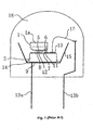
- Fig. 1 illustrates a packaged semiconductor LED, described in more detail in U.S. Patent 6,333,522.
- a III-nitride LED element 1 is formed on a transparent substrate 1a mounted face-down on a Si diode element 2 formed in a silicon substrate. Electrical connections between LED element 1 and diode element 2 are provided by gold microbumps 11 and 12 between a p-side electrode 5 of LED element 1 and an n-side electrode 8 of the Si diode element 2, and between an n-side electrode 6 of LED element 1 and a p-side electrode 7 of the Si diode element 2.
- the Si diode element 2 functions to protect LED element 1 from electrostatic discharge.
- the Si diode element 2 has a backside electrode 9 connected to a mount portion 15 of a lead frame 13a by a conductive paste 14.
- the p-side electrode 7 of the Si diode element 2 has a bonding pad portion 10 connected to a lead frame 13b by a gold wire bond 17.
- a transparent resin 18 covers LED element 1 and Si diode element 2.
- the package illustrated in Fig. 1 has several disadvantages.
- the package of Fig. 1 does not efficiently conduct heat away from LED element 1. Heat is generated within the LED during regular operation. Light is generated in the LED by electrons from the n-type region recombining with holes from the p-type region. Some of this recombination is radiative, leading to the emission of photons. A sizeable fraction of the recombination may be non-radiative, generating heat instead of photons. In addition, some of the photons generated by radiative recombination are absorbed within the device, creating additional heat. In some devices, at least some of the heat generated within the device must be conducted away from the die to avoid damaging the LED.
- Fig. 1 does not easily allow for multiple devices, such as multiple LED elements or chips containing other circuitry, to be connected to lead frames 13a and 13b.
- LEDs have operated at low power, for example, less than 300 mW.
- the problems with the package of Fig. 1 become severe design limitations as newer generations of LEDs are planned to be operated at higher power, for example, 1 W to 500 W, and in higher temperature environments, leading to an increase in operating temperatures and heat production.
- a semiconductor light emitting device package includes a substrate with a core and a copper layer overlying the core.
- the light emitting device is connected to the substrate directly or indirectly through a wiring substrate.
- the core of the substrate may be, for example, ceramic, Al 2 O 3 , AlN, alumina, or silicon nitride.
- the copper layer may be bonded to the core by a process such as direct bonding of copper or active metal brazing.
- the materials used in the package may be chosen to efficiently remove heat from the light emitting device, to have an insulating layer to facilitate mounting and connection of multiple chips, and to closely match the coefficient of thermal expansion (CTE) of the light emitting device and any intervening structure.
- CTE coefficient of thermal expansion
- a semiconductor light emitting device is mounted, directly or indirectly, on a substrate including a copper layer.
- the substrate may be chosen (1) to efficiently remove heat from the light emitting device, (2) to facilitate mounting and connection of multiple chips, and (3) to closely match the coefficient of thermal expansion (CTE) of the light emitting device and any intervening structure.
- CTE coefficient of thermal expansion
- Figs. 2 and 3 are a plan view and a cross sectional view of an embodiment of the invention.
- Semiconductor light emitting devices 20 are mounted on a substrate 30 including a thick copper layer (hereinafter referred to as a "copper substrate").
- Copper substrate 30 includes an insulating core 24 and one or more thick regions of the metal 25 and 29.
- Core layer 24 and metal regions 25 and 29 are selected such that the composite of core layer 24 and metal regions 25 and 29 has a coefficient of thermal expansion matched to LED 20 and to have high thermal conductivity.
- Core 24 may be, for example, ceramic, Al 2 O 3 , AlN, alumina, or silicon nitride.
- Metal regions 25 and 29 are often copper, but may be any suitable metal.
- Metal regions 25 and 29 are thick enough to efficiently conduct heat laterally, generally about 4 mils (101.6 ⁇ m) to about 24 mils (609.6 ⁇ m). Multiple metal regions 29 formed on the side of copper substrate 30 on which the LEDs are mounted electrically connect leads 27 to the LEDs.
- metal regions 29 are electrically isolated from each other by core 24. Though two metal regions 29 are illustrated in Fig. 2, more metal regions and more leads 27 may be provided where additional devices are provided on copper substrate 30. Metal region 25 on the opposite side of copper substrate 30 usually does not provide electrical connections and is thus an uninterrupted layer of metal.
- Metal layers 25 and 29 may be bonded to core layer 24 by processes known in the art such as direct bonding of copper (DBC) and active metal brazing (AMB).
- copper substrate 30 is a DBC substrate.
- DBC substrates are made by oxidizing a sheet of copper foil, then placing the foil on core layer 24 to form a composite substrate. The composite substrate is heated to a process temperature between about 1065 °C and 1083 °C to form a eutectic melt that creates a continuous, uniform bond between the core and the metal layer, then cooled to room temperature.
- the copper on the substrate may be lithographically patterned to form different regions. DBC substrates described in more detail in U.S.
- DBC substrates are available from Curamik Electronics of Germany. DBC substrates offer excellent thermal conductivity and coefficients of thermal expansion closely matched to III-nitride LEDs.
- a semiconductor light emitting device may have a coefficient of thermal expansion of about 5 ppm/K.
- a Cu/Al 2 O 3 /Cu DBC may have a thermal conductivity of about 24 W/m ⁇ K and a coefficient of thermal expansion of about 7.3 ppm/K.
- a Cu/A1N/Cu DBC substrate may have a thermal conductivity of about 180 W/m ⁇ K and a coefficient of thermal expansion of about 5.1 ppm/K.
- a standard metal core printed circuit board (MCPCB) with thin copper traces bonded to a dielectric layer with epoxy, then bonded to an aluminum layer with epoxy may have a thermal conductivity of only 2-5 W/m ⁇ K and a coefficient of thermal expansion of 25-30 ppm/K.
- DBC substrates may be processed and may operate at temperatures up to about 800 °C, in contrast to standard MCPCBs which can tolerate process temperatures up to only 250 °C and can be operated at temperatures up to only 140 °C.
- AMB substrates are formed by using a layer of braze to bond thick copper regions 25 and 29 to core 24, rather than the direct bond of a DBC substrate.
- Suitable AMB substrates with an A1N core are available from Toshiba.
- Light emitting devices 20 of Figs. 2 and 3 are usually high power devices, i.e. devices having an area greater than about 400x400 ⁇ m 2 and capable of operating at a current density of at least 50A/cm 2 .
- a common size for a high power device is an area greater than or equal to 1x1 mm 2 and electrical power consumption greater than or equal to 1W.
- the devices illustrated in Figs. 2 and 3 are flip chips, i.e. mounted with both contacts on the same side of the device and facing copper substrate 30 such that light is extracted through the side of the device opposite the contacts, other configurations are possible and within the scope of the invention. For example, rather than being mounted over two metal regions 29, LEDs 20 of Figs.
- a device suitable for wire bonding may be, for example, a III-nitride device formed on a conducting SiC substrate.
- Figs. 4-6 An example of a high power semiconductor light emitting device suitable for use with the package of Figs. 2 and 3 is illustrated in Figs. 4-6.
- the device of Figs. 4-6 is described in more detail in Application Serial No. 10/172,311, filed June 13, 2002 and incorporated herein by reference.
- Fig. 4 is a plan view;
- Fig. 5 is a cross sectional view along axis AA of Fig. 4;
- Fig. 6 is a cross sectional view along axis BB of Fig. 4.
- the semiconductor layers 31 of the device of Figs. 4-6 may be III-nitride layers grown on a transparent substrate, such as SiC or sapphire (not shown).
- layers 31 include an n-type region formed over the substrate, an active region formed over the n-type region, and a p-type region formed over the active region. Portions of the active and p-type regions are etched away to expose portions of the n-type region on which n-contacts 32 are formed.
- contact to the n-side of the device is made by a plurality of holes etched down to the n-type region of the device.
- the holes are connected by a series of interconnects formed over and electrically isolated from the p-contacts 33.
- Fig. 4 illustrates 16 n-contact holes, enclosing nine p-contact regions.
- P-contacts 33 are isolated from n-contacts 32 by one or more dielectric layers 35.
- the top dielectric layers are patterned to expose p-contacts 33, but not n-contacts 32.
- a p-interconnect region 37 is then deposited over the left hand side of the device.
- interconnect regions 36 and 37 facilitate contact between LED 20 and copper substrate 30. If the LED is solder-mounted to copper substrate 30, interconnect regions 36 and 37 may be, for example, solderable metals.
- the shape and placement of interconnect regions 36 and 37 is arbitrary with respect to the shape and placement of underlying contacts 32 and 33. Thus, interconnect regions 36 and 37 can be made large enough and far enough apart to permit direct connection to copper substrate 30.
- Leads 27, if used, may be connected metal regions 29 on copper substrate 30. Leads 27 may be straight, as shown, or formed for stress relief. The material used to form leads 27 may be thermally resistive, to facilitate soldering, spot welding, and attaching a slip-on connector to the leads. Other methods besides leads may be used to electrically and physically attach copper substrate 30 to another device. For example, in place of leads 27, solder pads, wire bonds, or terminated wires may be formed on metal regions 29. In general, leads or some other method of connecting copper substrate 30 to another device are used rather than directly connecting the device to one of the metal regions on copper substrate 30, because copper substrate 30 so efficiently conducts heat that it can be difficult to heat the metal regions of copper substrate 30 enough to wet a direct connector such as solder to the surface.
- Figs. 7 and 8 illustrate an alternative embodiment of the present invention.
- semiconductor light emitting devices 20 are mounted on an optional wiring substrate 23, rather than directly on copper substrate 30.
- Wiring substrate 23 and any other devices 21 included in the design are then mounted on copper substrate 30.
- Wiring substrate 23 may be used when the interconnect regions on LEDs 20 are sized, shaped, or placed in a manner that make direct connection to copper substrate impractical or impossible.
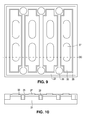
- An example of an LED with such interconnect regions is illustrated in Figs. 9 and 10.
- Fig. 9 is a plan view and Fig. 10 is a cross sectional view along line DD of Fig. 9.
- N-contact 32 is a single, continuous contact dividing the active region into four segments.
- P-contacts 33 are formed on the remaining portions of the p-type region.
- the n- and p-contacts are electrically isolated by air or an optional dielectric layer 35.
- N-interconnect regions 36 and p-interconnect regions 37 are formed on n-contacts 32 and p-contacts 33.
- interconnect regions correspond to the underlying contacts and must therefore be fairly small and carefully spaced.
- the size and spacing of interconnect regions 36 and 37 make it impractical to directly bond LED 20 to copper substrate 30, because it is difficult to form copper features of the size and spacing required by the device of Figs. 9 and 10 that are thick enough to have favorable heat spreading characteristics.
- LED 20 of Figs. 9 and 10 is mounted on wiring substrate 23.
- Wiring substrate 23 may be, for example, a metal/ceramic composite wiring substrate as described in U.S. Patent 6,413,620, which is incorporated herein by reference.
- the ceramic may be, for example, A1N or alumina, silicon nitride and the metal may be, for example tungsten or molybdenum.
- Suitable wiring substrates are available from Kyocera Corporation of Kyoto, Japan.
- Wiring substrate 23 may be formed with interconnect regions small enough to accommodate bonding to the interconnect regions of the device illustrated in Figs. 9 and 10. Multiple LEDs, fabricated either on the same growth substrate or on separate growth substrates, may be mounted on and electrically connected by wiring substrate, as illustrated in Fig.
- wiring substrate 23 is selected to be CTE matched to LED 20 and copper substrate 30, and to have high thermal conductivity to conduct heat away from LED 20.
- circuitry such as electrostatic discharge protection circuitry or power conditioning circuitry usually cannot be formed within wiring substrate 23 and is provided as separate chips 21, mounted either on wiring substrate 23 or directly on copper substrate 30.
- wiring substrate 23 is a silicon integrated circuit including any required circuitry.
- copper substrate 30 is connected to a base 26, which is used to connect copper substrate 30 to a heat sink or other device.
- the base shown in Fig. 7 has two notches that facilitate bolting or riveting base 26 to a heat sink, though solder or any other suitable technique may be used to attach base 26 to a heat sink.
- an interface material is disposed between base 26 and the heat sink on which base 26 is mounted, to channel heat from base 26 to the heat sink. Examples of such materials are thermal grease, phase change tape, solder, or a thermal blanket.
- the interface materials are typically poor thermal conductors. To improve the thermal performance of the interface and to facilitate bolting base 26 to the heat sink, the footprint of base 26 is often larger than copper substrate 30.
- the size of the footprint of base will also increase.
- the size of the footprint of the base can be selected to prevent the LEDs from exceeding a given maximum temperature.
- a lens 28 is formed over LED 20.
- Lens 28 may be, for example, a high index optical material bonded to LED 20, to wiring substrate 23, or to copper substrate 30.
- lens 28 may be a hard or soft silicone lens or a hard epoxy or other clear plastic lens molded over LED 20.
- a hard or soft silicone lens is coupled to one or more LEDs with a soft silicone gel or other optically transparent materials.
- a lens is formed over each LED chip. In the device illustrated in Figs. 7 and 8, each LED chip includes four individual LEDs.
- a lens may be formed or attached to each LED device, or a single lens may be formed or attached to all the LEDs in the device. Since hard plastic materials such as epoxy tend to have CTEs vastly different from LEDs (for example, 50-60 ppm/K for plastic vs. 5 ppm/K for a semiconductor device), a lens formed over all the LEDs in the device must usually be formed from a soft, flexible material, such as a silicone material. If the lens is formed over an individual chip or an individual device, hard materials such as epoxy may be used.
- the packaged devices illustrated in Figs. 2 and 3 or 7 and 8 may be assembled as follows. First, if a wiring substrate 23 is used, LED 20 is electrically and physically connected to wiring substrate 23 by any suitable bonding material including, for example, solder, elemental metals, metal alloys, semiconductor-metal alloys, thermally and electrically conductive pastes or compounds, eutectic joints, and gold stud-bumps. A lens 28 that is directly bonded to LED 20 may be mounted on LED 20 before LED 20 is connected to wiring substrate 23.
- Leads 27 and optional base 26 are then brazed to copper substrate 30, usually at a temperature of about 800 °C and in an atmosphere of nitrogen, rather than hydrogen or a mixture of hydrogen and nitrogen, to avoid damaging the oxide bond between the metal regions and the core of copper substrate 30.
- wiring substrate 23, or LED 20 if no wiring substrate is used, and any other required devices 21 are electrically and physically connected to copper substrate 30 by, for example, solder.
- the use of a substrate including a thick copper layer in a semiconductor light emitting device package may offer several advantages.
- the packages illustrated in Figs. 2, 3, 7 and 8 use highly thermally conductive materials, allowing the package to efficiently conduct heat away from LEDs 20.
- the package designs of Figs. 2, 3, 7 and 8 spread heat laterally in metal regions 29, and vertically through metal regions 29, core 24, and metal region 25. Laterally spreading the heat eliminates hot spots that may damage LEDs 20.
- the ability to efficiently channel heat away from LEDs 20 potentially permits higher current density operation without the risk of damage to the LEDs.
- insulating core 24 of copper substrate 30 permits electrical isolation of different metal regions 29, allowing multiple devices to be incorporated on a single substrate.
Landscapes
- Led Device Packages (AREA)
- Ceramic Products (AREA)
- Led Devices (AREA)
Abstract
Description
Claims (22)
- A structure comprising:wherein the semiconductor light emitting device is electrically connected to at least one of the copper layers.a semiconductor light emitting device; anda substrate comprising a ceramic core and at least one copper layer overlying the core, the at least one copper layer having a thickness of at least 4 mils;
- The structure of claim 1 wherein the semiconductor light emitting device comprises a III-nitride light emitting layer.
- The structure of claim 1 wherein the core comprises a material selected from the group of ceramic, Al2O3, AlN, alumina, and silicon nitride.
- The structure of claim 1 further comprising at least one lead connected to at least one of the copper layers.
- The structure of claim 1 further comprising at least one solder pad connected to at least one of the copper layers.
- The structure of claim 1 further comprising at least one terminated wire connected to at least one of the copper layers.
- The structure of claim 1 wherein the at least one copper layer is bonded to the core by a direct copper bond.
- The structure of claim 1 wherein the at least one copper layer is bonded to the core by an active metal braze.
- The structure of claim 1 wherein the at least one copper layer has a thickness between about 4 mils and about 24 mils.
- The structure of claim 1 wherein the substrate is a first substrate, the structure further comprising a second substrate disposed between the semiconductor light emitting device and the first substrate.
- The structure of claim 10 wherein the second substrate comprises at least one metal bonding pad and an insulating layer.
- The structure of claim 11 wherein the insulating layer comprises A1N.
- The structure of claim 10 wherein the second substrate comprises a silicon integrated circuit.
- The structure of claim 1 further comprising a base connected to the substrate.
- The structure of claim 1 further comprising a lens disposed over the semiconductor light emitting device.
- The structure of claim 1 wherein the copper layer is bonded to the core.
- The structure of claim 1 wherein the copper layer is bonded to the core by a process comprising:forming an oxide coating on a sheet of copper;placing the oxide coating adjacent to the core; andheating the oxide coating to form a eutectic melt.
- A method of packaging a semiconductor light emitting device, the method comprising:providing a substrate having a ceramic core and at least one copper layer, the at least one copper layer having a thickness of at least 4 mils; andelectrically connecting a semiconductor light emitting device to at least one of the copper layers.
- The method of claim 18 further comprising attaching at least one lead to the at least one copper layer.
- The method of claim 18 wherein the substrate is a first substrate, the method further comprising:mounting the semiconductor light emitting device on a second substrate; andafter mounting the semiconductor light emitting device on the second substrate, mounting the second substrate on the first substrate.
- The method of claim 18 further comprising:providing a lens over the semiconductor light emitting device.
- The method of claim 18 further comprising bonding the copper layer to the core by:forming an oxide coating on a sheet of copper;placing the oxide coating adjacent to the core; andheating the oxide coating to form a eutectic melt.
Applications Claiming Priority (2)
| Application Number | Priority Date | Filing Date | Title |
|---|---|---|---|
| US10/652,348 US7482638B2 (en) | 2003-08-29 | 2003-08-29 | Package for a semiconductor light emitting device |
| US652348 | 2003-08-29 |
Publications (2)
| Publication Number | Publication Date |
|---|---|
| EP1511090A2 true EP1511090A2 (en) | 2005-03-02 |
| EP1511090A3 EP1511090A3 (en) | 2009-12-09 |
Family
ID=34104746
Family Applications (1)
| Application Number | Title | Priority Date | Filing Date |
|---|---|---|---|
| EP04103856A Withdrawn EP1511090A3 (en) | 2003-08-29 | 2004-08-10 | Package for a semiconductor light emitting device |
Country Status (4)
| Country | Link |
|---|---|
| US (2) | US7482638B2 (en) |
| EP (1) | EP1511090A3 (en) |
| JP (2) | JP2005079593A (en) |
| TW (1) | TWI366280B (en) |
Cited By (3)
| Publication number | Priority date | Publication date | Assignee | Title |
|---|---|---|---|---|
| EP1923922A1 (en) * | 2006-11-15 | 2008-05-21 | Lemnis Lighting IP GmbH | Improved led lighting assembly |
| WO2009066099A1 (en) * | 2007-11-19 | 2009-05-28 | Wang Nang Wang | Led chip thermal management and fabrication methods |
| US7918596B2 (en) | 2007-04-20 | 2011-04-05 | Federal Signal Corporation | Warning light |
Families Citing this family (41)
| Publication number | Priority date | Publication date | Assignee | Title |
|---|---|---|---|---|
| US7355284B2 (en) * | 2004-03-29 | 2008-04-08 | Cree, Inc. | Semiconductor light emitting devices including flexible film having therein an optical element |
| WO2006059828A1 (en) * | 2004-09-10 | 2006-06-08 | Seoul Semiconductor Co., Ltd. | Light emitting diode package having multiple molding resins |
| US7748873B2 (en) * | 2004-10-07 | 2010-07-06 | Seoul Semiconductor Co., Ltd. | Side illumination lens and luminescent device using the same |
| US20060097385A1 (en) * | 2004-10-25 | 2006-05-11 | Negley Gerald H | Solid metal block semiconductor light emitting device mounting substrates and packages including cavities and heat sinks, and methods of packaging same |
| KR101115800B1 (en) * | 2004-12-27 | 2012-03-08 | 엘지디스플레이 주식회사 | Light-emitting device package, method for fabricating the same and backlight unit |
| US7754507B2 (en) * | 2005-06-09 | 2010-07-13 | Philips Lumileds Lighting Company, Llc | Method of removing the growth substrate of a semiconductor light emitting device |
| US7348212B2 (en) * | 2005-09-13 | 2008-03-25 | Philips Lumileds Lighting Company Llc | Interconnects for semiconductor light emitting devices |
| US7736945B2 (en) * | 2005-06-09 | 2010-06-15 | Philips Lumileds Lighting Company, Llc | LED assembly having maximum metal support for laser lift-off of growth substrate |
| JP4945106B2 (en) * | 2005-09-08 | 2012-06-06 | スタンレー電気株式会社 | Semiconductor light emitting device |
| WO2007122548A2 (en) * | 2006-04-20 | 2007-11-01 | Nxp B.V. | Thermal isolation of electronic devices in submount used for leds lighting applications |
| KR101258227B1 (en) * | 2006-08-29 | 2013-04-25 | 서울반도체 주식회사 | Light emitting device |
| US7700967B2 (en) | 2007-05-25 | 2010-04-20 | Philips Lumileds Lighting Company Llc | Illumination device with a wavelength converting element held by a support structure having an aperture |
| WO2009000105A1 (en) * | 2007-06-25 | 2008-12-31 | Jenshyan Chen | A light-emitting diode lighting device |
| US20090050921A1 (en) * | 2007-08-23 | 2009-02-26 | Philips Lumileds Lighting Company Llc | Light Emitting Diode Array |
| JP5056327B2 (en) * | 2007-10-10 | 2012-10-24 | 日亜化学工業株式会社 | Light emitting device |
| US20090154137A1 (en) * | 2007-12-14 | 2009-06-18 | Philips Lumileds Lighting Company, Llc | Illumination Device Including Collimating Optics |
| US8127445B2 (en) * | 2008-04-03 | 2012-03-06 | E. I. Du Pont De Nemours And Company | Method for integrating heat transfer members, and an LED device |
| JP5304198B2 (en) | 2008-11-24 | 2013-10-02 | 東芝ライテック株式会社 | lighting equipment |
| KR101020910B1 (en) * | 2008-12-24 | 2011-03-09 | 엘지이노텍 주식회사 | Semiconductor light emitting device and manufacturing method thereof |
| JP2010272736A (en) * | 2009-05-22 | 2010-12-02 | Toshiba Lighting & Technology Corp | Light-emitting device |
| JP4957927B2 (en) | 2009-05-29 | 2012-06-20 | 東芝ライテック株式会社 | Light bulb shaped lamp and lighting equipment |
| US20110065218A1 (en) * | 2009-09-14 | 2011-03-17 | Bridgelux Inc. | Pre-thermal greased led array |
| JP5375552B2 (en) * | 2009-11-24 | 2013-12-25 | 東芝ライテック株式会社 | LIGHT EMITTING DEVICE AND LIGHTING APPARATUS HAVING THE SAME |
| EP2315284A3 (en) * | 2009-10-21 | 2013-03-27 | Toshiba Lighting & Technology Corporation | Light-Emitting apparatus and luminaire |
| WO2011083923A2 (en) | 2010-01-07 | 2011-07-14 | Seoul Opto Device Co., Ltd. | Light emitting diode having electrode pads |
| KR101242218B1 (en) | 2011-01-07 | 2013-03-11 | 에이텍 테크놀로지 코포레이션 | Lighting device and method for forming the same |
| US8982558B2 (en) * | 2011-06-24 | 2015-03-17 | General Electric Company | Cooling device for a power module, and a related method thereof |
| US9510413B2 (en) | 2011-07-28 | 2016-11-29 | Cree, Inc. | Solid state lighting apparatus and methods of forming |
| US9131561B2 (en) | 2011-09-16 | 2015-09-08 | Cree, Inc. | Solid-state lighting apparatus and methods using energy storage |
| US9277605B2 (en) | 2011-09-16 | 2016-03-01 | Cree, Inc. | Solid-state lighting apparatus and methods using current diversion controlled by lighting device bias states |
| CN103907401B (en) * | 2011-07-28 | 2017-08-29 | 克里公司 | Solid state light emitting device and method of forming |
| US8742671B2 (en) | 2011-07-28 | 2014-06-03 | Cree, Inc. | Solid state lighting apparatus and methods using integrated driver circuitry |
| US8791641B2 (en) | 2011-09-16 | 2014-07-29 | Cree, Inc. | Solid-state lighting apparatus and methods using energy storage |
| US9609709B2 (en) | 2012-08-21 | 2017-03-28 | Cree, Inc. | Multi-segment LED components and LED lighting apparatus including the same |
| US9131571B2 (en) | 2012-09-14 | 2015-09-08 | Cree, Inc. | Solid-state lighting apparatus and methods using energy storage with segment control |
| RU2561240C2 (en) * | 2013-05-15 | 2015-08-27 | Евгений Иванович Челноков | Fabrication of ic case |
| US20150257316A1 (en) * | 2014-03-07 | 2015-09-10 | Bridge Semiconductor Corporation | Method of making thermally enhanced wiring board having isolator incorporated therein |
| FR3038535B1 (en) * | 2015-07-10 | 2017-08-11 | Commissariat Energie Atomique | ASSEMBLY COMPRISING TWO DIFFERENT THERMAL EXPANSION COEFFICIENT ELEMENTS AND A DENSITY HETEROGENEOUS FRITTE JOINT AND METHOD OF MANUFACTURING THE ASSEMBLY |
| EP3290399B1 (en) | 2016-08-29 | 2022-03-02 | Infineon Technologies AG | Method for producing a metal-ceramic substrate with a least one via |
| US11592166B2 (en) | 2020-05-12 | 2023-02-28 | Feit Electric Company, Inc. | Light emitting device having improved illumination and manufacturing flexibility |
| US11876042B2 (en) | 2020-08-03 | 2024-01-16 | Feit Electric Company, Inc. | Omnidirectional flexible light emitting device |
Family Cites Families (32)
| Publication number | Priority date | Publication date | Assignee | Title |
|---|---|---|---|---|
| US4012833A (en) * | 1973-12-28 | 1977-03-22 | Sony Corporation | Method of making display structure having light emitting diodes |
| US4566170A (en) * | 1983-05-10 | 1986-01-28 | Pitney Bowes Inc. | Method of producing a light emiting diode array |
| US4735866A (en) | 1985-12-30 | 1988-04-05 | The United States Of America As Represented By The United States Department Of Energy | Copper-silver-titanium-tin filler metal for direct brazing of structural ceramics |
| JPH03171682A (en) * | 1989-11-29 | 1991-07-25 | Iwasaki Electric Co Ltd | Light emitting diode |
| JP2501272B2 (en) * | 1992-07-15 | 1996-05-29 | 株式会社東芝 | Multilayer ceramic circuit board |
| DE4233073A1 (en) * | 1992-10-01 | 1994-04-07 | Siemens Ag | Semiconductor modular structure prodn. - by convexly shaping and bonding in single hot pressing operation |
| JP2781329B2 (en) * | 1992-10-21 | 1998-07-30 | 三菱電機株式会社 | Semiconductor power module and method of manufacturing the same |
| DE19614501C2 (en) | 1996-04-13 | 2000-11-16 | Curamik Electronics Gmbh | Process for producing a ceramic-metal substrate and ceramic-metal substrate |
| JPH09307145A (en) * | 1996-05-13 | 1997-11-28 | Nichia Chem Ind Ltd | Optical semiconductor device |
| CN1300859C (en) | 1997-01-31 | 2007-02-14 | 松下电器产业株式会社 | Light emitting element |
| JPH1146018A (en) * | 1997-07-28 | 1999-02-16 | Citizen Electron Co Ltd | Surface mount type light emitting diode |
| US6093443A (en) | 1997-11-12 | 2000-07-25 | Curamik Electronics Gmbh | Process for producing a ceramic-metal substrate |
| US6404065B1 (en) * | 1998-07-31 | 2002-06-11 | I-Xys Corporation | Electrically isolated power semiconductor package |
| JP2000058995A (en) * | 1998-08-11 | 2000-02-25 | Sumitomo Kinzoku Electro Device:Kk | Ceramic circuit board and semiconductor module |
| US6274924B1 (en) | 1998-11-05 | 2001-08-14 | Lumileds Lighting, U.S. Llc | Surface mountable LED package |
| US6413620B1 (en) | 1999-06-30 | 2002-07-02 | Kyocera Corporation | Ceramic wiring substrate and method of producing the same |
| JP2001015895A (en) * | 1999-06-30 | 2001-01-19 | Kyocera Corp | Wiring board and method of manufacturing the same |
| US6486499B1 (en) | 1999-12-22 | 2002-11-26 | Lumileds Lighting U.S., Llc | III-nitride light-emitting device with increased light generating capability |
| JP3603725B2 (en) * | 2000-03-02 | 2004-12-22 | 日本電気株式会社 | Semiconductor device, method of manufacturing the same, and circuit board |
| JP2002118294A (en) * | 2000-04-24 | 2002-04-19 | Nichia Chem Ind Ltd | Flip chip type light emitting diode and manufacturing method |
| DE10146227B4 (en) * | 2000-09-20 | 2015-01-29 | Hitachi Metals, Ltd. | Silicon nitride sintered body, printed circuit board and thermoelectric module |
| JP2002164475A (en) * | 2000-11-24 | 2002-06-07 | Nitto Denko Corp | Semiconductor device |
| JP2002203942A (en) * | 2000-12-28 | 2002-07-19 | Fuji Electric Co Ltd | Power semiconductor module |
| US6786651B2 (en) * | 2001-03-22 | 2004-09-07 | Primarion, Inc. | Optical interconnect structure, system and transceiver including the structure, and method of forming the same |
| TW492202B (en) | 2001-06-05 | 2002-06-21 | South Epitaxy Corp | Structure of III-V light emitting diode (LED) arranged in flip chip configuration having structure for preventing electrostatic discharge |
| KR100843734B1 (en) * | 2001-09-27 | 2008-07-04 | 페어차일드코리아반도체 주식회사 | Semiconductor power module and manufacturing method |
| US6498355B1 (en) * | 2001-10-09 | 2002-12-24 | Lumileds Lighting, U.S., Llc | High flux LED array |
| US6480389B1 (en) * | 2002-01-04 | 2002-11-12 | Opto Tech Corporation | Heat dissipation structure for solid-state light emitting device package |
| TW577178B (en) * | 2002-03-04 | 2004-02-21 | United Epitaxy Co Ltd | High efficient reflective metal layer of light emitting diode |
| US6642550B1 (en) * | 2002-08-26 | 2003-11-04 | California Micro Devices | Silicon sub-mount capable of single wire bonding and of providing ESD protection for light emitting diode devices |
| JP3991961B2 (en) * | 2002-09-05 | 2007-10-17 | 日亜化学工業株式会社 | Side-emitting type light emitting device |
| JP3636706B2 (en) * | 2002-12-20 | 2005-04-06 | イビデン株式会社 | Ceramic DBC substrate |
-
2003
- 2003-08-29 US US10/652,348 patent/US7482638B2/en not_active Expired - Lifetime
-
2004
- 2004-08-10 EP EP04103856A patent/EP1511090A3/en not_active Withdrawn
- 2004-08-26 TW TW093125630A patent/TWI366280B/en not_active IP Right Cessation
- 2004-08-27 JP JP2004248839A patent/JP2005079593A/en active Pending
-
2009
- 2009-01-23 US US12/359,166 patent/US7759144B2/en not_active Expired - Lifetime
-
2011
- 2011-06-21 JP JP2011137629A patent/JP2011193026A/en not_active Abandoned
Cited By (4)
| Publication number | Priority date | Publication date | Assignee | Title |
|---|---|---|---|---|
| EP1923922A1 (en) * | 2006-11-15 | 2008-05-21 | Lemnis Lighting IP GmbH | Improved led lighting assembly |
| WO2008059033A3 (en) * | 2006-11-15 | 2008-07-10 | Lemnis Lighting Ip Gmbh | Improved led lighting assembly |
| US7918596B2 (en) | 2007-04-20 | 2011-04-05 | Federal Signal Corporation | Warning light |
| WO2009066099A1 (en) * | 2007-11-19 | 2009-05-28 | Wang Nang Wang | Led chip thermal management and fabrication methods |
Also Published As
| Publication number | Publication date |
|---|---|
| TW200514282A (en) | 2005-04-16 |
| EP1511090A3 (en) | 2009-12-09 |
| TWI366280B (en) | 2012-06-11 |
| US7759144B2 (en) | 2010-07-20 |
| US20050045901A1 (en) | 2005-03-03 |
| US7482638B2 (en) | 2009-01-27 |
| JP2011193026A (en) | 2011-09-29 |
| US20090170226A1 (en) | 2009-07-02 |
| JP2005079593A (en) | 2005-03-24 |
Similar Documents
| Publication | Publication Date | Title |
|---|---|---|
| US7759144B2 (en) | Package for a semiconductor light emitting device | |
| US6876008B2 (en) | Mount for semiconductor light emitting device | |
| US8987769B2 (en) | High thermal performance packaging for optoelectronics devices | |
| JP5462433B2 (en) | Semiconductor light emitting device having integrated electronic components | |
| US8101966B2 (en) | Light-emitting diode lamp with low thermal resistance | |
| US8309979B2 (en) | Electrically isolated vertical light emitting diode structure | |
| US7161190B2 (en) | Semiconductor light-emitting device and method of manufacturing the same | |
| US9443903B2 (en) | Low temperature high strength metal stack for die attachment | |
| EP2428991B1 (en) | Light Emitting Component with integrated control | |
| US20090153007A1 (en) | Light source module and method for manufacturing same | |
| US8373195B2 (en) | Light-emitting diode lamp with low thermal resistance | |
| JP2012515440A (en) | Multiple light emitting device package | |
| JPH10321909A (en) | Semiconductor device | |
| EP1878052B1 (en) | Light emitting diode structure | |
| TW201131829A (en) | Thermally-enhanced hybrid LED package components | |
| US20100224890A1 (en) | Light emitting diode chip with electrical insulation element | |
| US7943430B2 (en) | Semiconductor device with heat sink and method for manufacturing the same | |
| CN101587925A (en) | Packaging structure of light-emitting element and manufacturing method thereof | |
| TWI901979B (en) | Wafer level fabrication for multiple chip light-emitting devices | |
| US20080090334A1 (en) | Method for Manufacturing Semiconductor Device | |
| GB2551154B (en) | Light-emitting diode package and method of manufacture | |
| EP3465780B1 (en) | Light-emitting device and method of manufacture |
Legal Events
| Date | Code | Title | Description |
|---|---|---|---|
| PUAI | Public reference made under article 153(3) epc to a published international application that has entered the european phase |
Free format text: ORIGINAL CODE: 0009012 |
|
| AK | Designated contracting states |
Kind code of ref document: A2 Designated state(s): AT BE BG CH CY CZ DE DK EE ES FI FR GB GR HU IE IT LI LU MC NL PL PT RO SE SI SK TR |
|
| AX | Request for extension of the european patent |
Extension state: AL HR LT LV MK |
|
| RAP1 | Party data changed (applicant data changed or rights of an application transferred) |
Owner name: PHILIPS LUMILEDS LIGHTING COMPANY LLC |
|
| PUAL | Search report despatched |
Free format text: ORIGINAL CODE: 0009013 |
|
| AK | Designated contracting states |
Kind code of ref document: A3 Designated state(s): AT BE BG CH CY CZ DE DK EE ES FI FR GB GR HU IE IT LI LU MC NL PL PT RO SE SI SK TR |
|
| AX | Request for extension of the european patent |
Extension state: AL HR LT LV MK |
|
| 17P | Request for examination filed |
Effective date: 20100609 |
|
| AKX | Designation fees paid |
Designated state(s): DE |
|
| RBV | Designated contracting states (corrected) |
Designated state(s): AT BE BG CH CY CZ DE DK EE ES FI FR GB GR HU IE IT LI LU MC NL PL PT RO SE SI SK TR |
|
| 17Q | First examination report despatched |
Effective date: 20120206 |
|
| STAA | Information on the status of an ep patent application or granted ep patent |
Free format text: STATUS: THE APPLICATION IS DEEMED TO BE WITHDRAWN |
|
| 18D | Application deemed to be withdrawn |
Effective date: 20120619 |