EP1511082A1 - Inhaltsadressierbare Speicherzelle (CAM) mit schwebendem Gatter und deren Herstellungsverfahren - Google Patents
Inhaltsadressierbare Speicherzelle (CAM) mit schwebendem Gatter und deren Herstellungsverfahren Download PDFInfo
- Publication number
- EP1511082A1 EP1511082A1 EP03425565A EP03425565A EP1511082A1 EP 1511082 A1 EP1511082 A1 EP 1511082A1 EP 03425565 A EP03425565 A EP 03425565A EP 03425565 A EP03425565 A EP 03425565A EP 1511082 A1 EP1511082 A1 EP 1511082A1
- Authority
- EP
- European Patent Office
- Prior art keywords
- floating gate
- gate electrode
- memory cells
- memory cell
- cam memory
- Prior art date
- Legal status (The legal status is an assumption and is not a legal conclusion. Google has not performed a legal analysis and makes no representation as to the accuracy of the status listed.)
- Granted
Links
- 238000007667 floating Methods 0.000 title claims abstract description 71
- 238000004519 manufacturing process Methods 0.000 title claims abstract description 29
- 239000011159 matrix material Substances 0.000 title claims abstract description 15
- 238000000034 method Methods 0.000 claims abstract description 24
- 239000000758 substrate Substances 0.000 claims abstract description 17
- 239000004065 semiconductor Substances 0.000 claims abstract description 16
- 230000015572 biosynthetic process Effects 0.000 claims description 2
- 238000000206 photolithography Methods 0.000 claims 2
- 229910021420 polycrystalline silicon Inorganic materials 0.000 description 9
- 229920005591 polysilicon Polymers 0.000 description 9
- 230000008878 coupling Effects 0.000 description 7
- 238000010168 coupling process Methods 0.000 description 7
- 238000005859 coupling reaction Methods 0.000 description 7
- 238000005530 etching Methods 0.000 description 4
- 238000000151 deposition Methods 0.000 description 2
- 230000008021 deposition Effects 0.000 description 2
- 230000000694 effects Effects 0.000 description 2
- 239000007943 implant Substances 0.000 description 2
- 238000001465 metallisation Methods 0.000 description 2
- 150000004767 nitrides Chemical class 0.000 description 2
- 238000005516 engineering process Methods 0.000 description 1
Images


Classifications
-
- H—ELECTRICITY
- H10—SEMICONDUCTOR DEVICES; ELECTRIC SOLID-STATE DEVICES NOT OTHERWISE PROVIDED FOR
- H10B—ELECTRONIC MEMORY DEVICES
- H10B41/00—Electrically erasable-and-programmable ROM [EEPROM] devices comprising floating gates
- H10B41/30—Electrically erasable-and-programmable ROM [EEPROM] devices comprising floating gates characterised by the memory core region
-
- H—ELECTRICITY
- H10—SEMICONDUCTOR DEVICES; ELECTRIC SOLID-STATE DEVICES NOT OTHERWISE PROVIDED FOR
- H10B—ELECTRONIC MEMORY DEVICES
- H10B69/00—Erasable-and-programmable ROM [EPROM] devices not provided for in groups H10B41/00 - H10B63/00, e.g. ultraviolet erasable-and-programmable ROM [UVEPROM] devices
-
- H—ELECTRICITY
- H10—SEMICONDUCTOR DEVICES; ELECTRIC SOLID-STATE DEVICES NOT OTHERWISE PROVIDED FOR
- H10D—INORGANIC ELECTRIC SEMICONDUCTOR DEVICES
- H10D64/00—Electrodes of devices having potential barriers
- H10D64/01—Manufacture or treatment
- H10D64/031—Manufacture or treatment of data-storage electrodes
- H10D64/035—Manufacture or treatment of data-storage electrodes comprising conductor-insulator-conductor-insulator-semiconductor structures
Definitions
- the present invention relates to a CAM (Content Addressable Matrix) memory cell and corresponding manufacturing process.
- the invention relates to a CAM memory cell integrated on a semiconductor substrate of the type comprising a plurality of floating gate memory cells, matrix-organised in rows, called word lines, and columns, called bit lines, said cells belonging to a same row and having floating gate electrodes being short-circuited with each other in order to form a single floating gate electrode for said memory cell of the CAM type.
- the invention also relates to a process for manufacturing memory cells of the CAM type integrated on a semiconductor substrate.
- the invention particularly relates, but not exclusively, to a CAM (Content Addressable Matrix) memory cell integrated on a semiconductor substrate and having a single floating gate electrode and the following description is made with reference to this field of application for convenience of illustration only.
- CAM Content Addressable Matrix
- EPROM or FLASH-EPROM electronic memory devices integrated on a semiconductor substrate comprise a plurality of matrix-organised non volatile memory cells; i.e. the cells are organised in rows, called word lines, and columns, called bit lines.
- a vertical section along a word line is shown, of a plurality of non volatile memory cells 1 integrated on a semiconductor substrate 2.
- each single non volatile memory cell 1 is manufactured in correspondence with a respective active area 1b which is insulated from an adjacent cell along a same word line by means of a thick oxide layer 3.
- Each single cell 1 comprises a MOS transistor wherein the gate electrode 4, located above a channel region and insulated therefrom by means of a thin oxide layer 5, is floating, i.e. it has a high DC impedance towards all the other terminals of the same cell and of the circuit wherein the cell is inserted.
- the cell 1 also comprises a second electrode 6, called control gate, which is coupled to the floating gate electrode 4 and insulated therefrom by means of an interpoly oxide layer 7.
- the control gate terminal 6, as it is known, is driven by convenient control voltages.
- the other electrodes of the MOS transistor comprised in the cell 1 are the usual drain, source and body terminals.
- EPROM or FLASH-EPROM electronic memory devices can comprise memory cells of the CAM (Content Addressable Matrix) type, usually used to store configuration information and to use redundancy in electronic memory devices.
- CAM memory cells are manufactured by using a plurality of traditional memory cells and they have a common floating gate terminal hanging over a plurality of channel regions of these traditional cells.
- CAM memory cells are generally gathered in a sub-matrix separated from the memory matrix.
- CAM cells are organised in rows, called word lines, and columns, called bit lines.
- FIG. 1 A known configuration of a CAM memory cell is shown in figure 2, represented in vertical section, along a word line, and globally indicated with 8.
- the CAM memory cell 8 comprises five traditional memory cells whose floating gate electrodes are short-circuited with each other to form a single floating gate electrode 9.
- N-1 are short-circuited with each other and used for reading operations, the remaining drain electrode being available for programming operations.
- the other body and source electrodes are common to all the cells belonging to the same CAM memory cell, similarly to what happens for the cells of a traditional memory device.
- a thick oxide layer 3a is formed on a semiconductor substrate 2 to define active areas 3b of the memory cell 8 as shown in figure 3.
- a thin gate oxide layer 5a of the memory cell 8 is grown, and a first polysilicon layer, called POLY 1, is then deposited and doped.
- the first polysilicon layer POLY 1 is etched to define a first size C, along word lines, of the single floating gate electrode 9 of the CAM memory cell 8.
- a first photolithographic mask 9a is used, shown in figure 4.
- a second size D of the single floating gate electrode 9 is then defined by using a second photolithographic mask 9b, as shown in figure 5.
- Figure 6 shows instead an overlapping of the masks 9a and 9b being used wherein the outlines of a plurality of single floating gate electrodes 9 of CAM memory cells 8 are highlighted with thick strokes.
- the prior art manufacturing process also comprises, traditionally after defining the single floating gate electrodes 9, the growth of an interpoly oxide layer 7a, typically comprising a series of oxide/nitride/oxide layers, called ONO, and the deposition and further etching of a second polysilicon layer to define a control gate electrode 6a of the CAM memory cell 8, as shown in figure 2.
- an interpoly oxide layer 7a typically comprising a series of oxide/nitride/oxide layers, called ONO
- a second polysilicon layer to define a control gate electrode 6a of the CAM memory cell 8, as shown in figure 2.
- the implants for manufacturing the source and drain electrodes of CAM cells 8 formed on the substrate 2a are then manufactured.
- the memory device is then completed by means of convenient metallisation layers.
- the ONO layer 7a area between polysilicon layers, POLY 1 and POLY 2, of the CAM memory cell 8, being said area represented in figure 2 along a size and being the other size given by the length D of the single floating gate electrode 9, is smaller than the corresponding area of the sum of the ONO layers 7 of five traditional matrix cells due to the contributions of the thickness A and of the distance B between the electrodes 4 of traditional memory cells 1.
- the capacity C PP,CAM of the CAM memory cell 8 between the first and second polysilicon layer which is proportional to the area of the ONO layer 7a covering the floating gate electrode 9, is lower than the capacity C PP,5MatrixCells between the first and second polysilicon layer of five traditional memory cells 1.
- the known configuration of CAM memory cells 8 thus implies less efficient performances, mainly a considerable extension of cancellation times with respect to a traditional cell 1.
- the technical problem underlying the present invention is to provide a CAM memory cell, having such structural and functional features as to provide a capacitive coupling ⁇ G similar to the one of a traditional memory cell, overcoming the limits and drawbacks still affecting prior art memory devices.
- the solution idea underlying the present invention is to manufacture a CAM memory cell having a single floating electrode, obtained by short-circuiting floating gate electrodes of traditional memory cells being adjacent with each other and belonging to a same word line, wherein the single floating gate electrode is equipped with cavities.
- CAM Content Addressable Matrix
- CAM memory cells are matrix-organised inside a memory device; i.e. these cells are organised in rows, called word lines, and columns, called bit lines.
- a CAM memory cell 10 manufactured according to the invention and integrated on a semiconductor substrate 11 is now described, which comprises a plurality of traditional memory cells 12.
- the CAM memory cell 10 comprises five traditional memory cells 12, belonging to the same word line and each one is manufactured in a respective active area 13 delimited by a thick insulating layer 14.
- Each traditional memory cell 12 comprises a MOS transistor having a floating gate electrode insulated from the semiconductor substrate 11 by means of a thin insulating layer 15 and respective source and drain electrodes manufactured in the semiconductor substrate 11.
- the five floating gate electrodes of the memory cells 12 are also short-circuited with each other in order to form a single floating gate electrode 16 of the CAM memory cell 10.
- drain electrodes of the memory cells 12 are short-circuited with each other and used to read the CAM memory cell 10, while the remaining drain electrode is used to program this CAM memory cell 10.
- the other body and source electrodes are common to all the CAM cells 10 belonging to the same matrix, similarly to what happens for traditional memory cell devices.
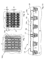
- the floating gate electrode 16 has at least a cavity 17 on the side walls as shown in figure 16.
- the floating gate electrode 16 has a plurality of cavities 17 manufactured in correspondence with the thick insulating layer 14.
- the depth P is substantially equal to half the length of the floating gate electrode 16, i.e. P ⁇ L/2.
- cavities 17 are manufactured alternatively in correspondence with a side of the CAM memory cells 10 wherein the source and drain electrodes are manufactured.
- An interpoly insulating layer 18, for example an ONO layer, covers the floating gate electrode 16 and it coats cavities 17.
- a second conductive layer 19a for example a polysilicon layer called POLY 2, formed on the interpoly insulating layer 18 manufactures the control gate electrode 19 of the CAM memory cell 10.
- the area of the interpoly insulating layer 18 of the CAM memory cell 10 is increased.
- present technologies do have a net area gain up to 20-30% which increases the capacitive coupling of the CAM memory cell 10 bringing it back to values close to the traditional memory cell 1 values.
- cavities 17 are manufactured only in correspondence with the side of the cell 10 wherein the source electrode is manufactured or only in correspondence with the side of the cell 10 wherein the drain electrode is manufactured.
- this embodiment requires a much higher precision in mask alignment since, even for small misalignments, an unacceptable leakage of the capacitive coupling values occurs.
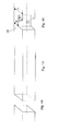
- cavities 17 are symmetrically manufactured on both sides of the floating gate electrode 16 and they have a depth P1.
- the presence of symmetrical cavities with depth P1 in the floating gate electrodes 16 allows the effect of a possible mask misalignment for values lower than P1 to be partially nullified.
- the distance S between two symmetrical cavities must be equal to the minimum length on the floating gate electrode 16, and it must be sufficiently lower than the length L of this electrode in order to allow deposition in the cavities 17 of the conductive layer 19a and in the meantime sufficiently thick to resist to etching after the definition of the control gate electrode 19.
- a thick insulating layer 14, for example oxide, is formed on a semiconductor substrate 11 in order to define active areas 13 of floating gate memory cells 12.
- a first conductive layer 16a for example a polysilicon layer called POLY 1
- the first conductive layer 16a is etched to define a first size E, along the word lines, of a single floating gate electrode 16 of the CAM memory cell 10.
- the first photolithographic mask 16b comprises a plurality of openings 16c which are partially aligned with portions of the first conductive layer 16a which will form the single final floating gate electrode 16. Therefore, during the etching step of the first conductive layer 16a, those portions of the first conductive layer 16a being exposed from openings 16c are also removed.
- these openings 16c are manufactured in correspondence with the thick insulating layer 14.
- the second size L of the single floating gate electrode 16 is then defined through a traditional photolithographic technique which uses a second photolithographic mask 16d, shown in figure 9.
- the single floating gate electrode 16 is then formed, equipped with cavities 17 on the side walls obtained by removing the first conductive layer 16a in correspondence with openings 16c.
- Figure 10 shows an overlapping of the masks used in the process according to the invention wherein the outlines of the floating gate electrodes 16 of CAM memory cells 10 according to the invention have been highlighted with thick strokes.
- Figure 12 shows a mask overlapping similarly to figure 10.
- the manufacturing process according to the invention provides then the formation of an interpoly insulating layer 18 on the floating gate electrode 16.
- the interpoly insulating layer 18 is for example an oxide layer typically comprising a series of oxide/nitride/oxide layers, called ONO.
- a control gate electrode 19 is then defined, realised by means of a second conductive layer 19a.
- the implants for manufacturing the source and drain electrodes of CAM cells 10 are then realised.
- the memory device is then completed by means of convenient metallisation levels.
- CAM memory cells according to the invention allow reduced cancellation times and generally more efficient performances to be obtained, in line with traditional matrix cells.
Landscapes
- Non-Volatile Memory (AREA)
- Semiconductor Memories (AREA)
Priority Applications (3)
| Application Number | Priority Date | Filing Date | Title |
|---|---|---|---|
| EP03425565A EP1511082B1 (de) | 2003-08-29 | 2003-08-29 | Inhaltsadressierbare Speicherzelle (CAM) mit schwebendem Gatter und deren Herstellungsverfahren |
| DE60309164T DE60309164D1 (de) | 2003-08-29 | 2003-08-29 | Inhaltsadressierbare Speicherzelle (CAM) mit schwebendem Gatter und deren Herstellungsverfahren |
| US10/926,785 US7285816B2 (en) | 2003-08-29 | 2004-08-26 | Content addressable matrix memory cell |
Applications Claiming Priority (1)
| Application Number | Priority Date | Filing Date | Title |
|---|---|---|---|
| EP03425565A EP1511082B1 (de) | 2003-08-29 | 2003-08-29 | Inhaltsadressierbare Speicherzelle (CAM) mit schwebendem Gatter und deren Herstellungsverfahren |
Publications (2)
| Publication Number | Publication Date |
|---|---|
| EP1511082A1 true EP1511082A1 (de) | 2005-03-02 |
| EP1511082B1 EP1511082B1 (de) | 2006-10-18 |
Family
ID=34089798
Family Applications (1)
| Application Number | Title | Priority Date | Filing Date |
|---|---|---|---|
| EP03425565A Expired - Lifetime EP1511082B1 (de) | 2003-08-29 | 2003-08-29 | Inhaltsadressierbare Speicherzelle (CAM) mit schwebendem Gatter und deren Herstellungsverfahren |
Country Status (3)
| Country | Link |
|---|---|
| US (1) | US7285816B2 (de) |
| EP (1) | EP1511082B1 (de) |
| DE (1) | DE60309164D1 (de) |
Families Citing this family (3)
| Publication number | Priority date | Publication date | Assignee | Title |
|---|---|---|---|---|
| US7986535B2 (en) * | 2007-07-17 | 2011-07-26 | Raytheon Company | Methods and apparatus for a cascade converter using series resonant cells with zero voltage switching |
| US7839023B2 (en) | 2007-07-18 | 2010-11-23 | Raytheon Company | Methods and apparatus for three-phase inverter with reduced energy storage |
| US8692310B2 (en) | 2009-02-09 | 2014-04-08 | Spansion Llc | Gate fringing effect based channel formation for semiconductor device |
Citations (2)
| Publication number | Priority date | Publication date | Assignee | Title |
|---|---|---|---|---|
| JPS6018953A (ja) * | 1983-07-12 | 1985-01-31 | Seiko Epson Corp | 半導体集積回路 |
| US5515320A (en) * | 1994-07-28 | 1996-05-07 | Nec Corporation | Non-volatile memory |
Family Cites Families (2)
| Publication number | Priority date | Publication date | Assignee | Title |
|---|---|---|---|---|
| EP0453863A2 (de) * | 1990-04-27 | 1991-10-30 | National Semiconductor Corporation | Verfahren und Gerät zur Ausführung einer Mediumzugriffssteuerung/Wirtsystemschnittstelle |
| KR100317492B1 (ko) * | 1999-12-28 | 2001-12-24 | 박종섭 | 플래쉬 메모리 소자의 코드저장 셀 |
-
2003
- 2003-08-29 DE DE60309164T patent/DE60309164D1/de not_active Expired - Lifetime
- 2003-08-29 EP EP03425565A patent/EP1511082B1/de not_active Expired - Lifetime
-
2004
- 2004-08-26 US US10/926,785 patent/US7285816B2/en not_active Expired - Lifetime
Patent Citations (2)
| Publication number | Priority date | Publication date | Assignee | Title |
|---|---|---|---|---|
| JPS6018953A (ja) * | 1983-07-12 | 1985-01-31 | Seiko Epson Corp | 半導体集積回路 |
| US5515320A (en) * | 1994-07-28 | 1996-05-07 | Nec Corporation | Non-volatile memory |
Non-Patent Citations (1)
| Title |
|---|
| PATENT ABSTRACTS OF JAPAN vol. 009, no. 136 (E - 320) 12 June 1985 (1985-06-12) * |
Also Published As
| Publication number | Publication date |
|---|---|
| US7285816B2 (en) | 2007-10-23 |
| EP1511082B1 (de) | 2006-10-18 |
| DE60309164D1 (de) | 2006-11-30 |
| US20050230739A1 (en) | 2005-10-20 |
Similar Documents
| Publication | Publication Date | Title |
|---|---|---|
| US20070184615A1 (en) | Process for Manufacturing a Non-Volatile Memory Electronic Device Integrated on a Semiconductor Substrate and Corresponding Device | |
| US6413821B1 (en) | Method of fabricating semiconductor device including nonvolatile memory and peripheral circuit | |
| US8227850B2 (en) | Gated semiconductor device and method of fabricating same | |
| US5688705A (en) | Method for reducing the spacing between the horizontally adjacent floating gates of a flash EPROM array | |
| US6627491B2 (en) | Method of manufacturing non volatile memory device having two charge storage regions | |
| JPH03505147A (ja) | デジタル及びアナログ2重レベル金属mos工程に適用する不揮発性工程 | |
| CN117202664B (zh) | 三维存储器及其制造方法、电子设备 | |
| KR20000053579A (ko) | 반도체 장치의 제조 방법, 불휘발성 반도체 메모리 장치및 그 제조 방법 | |
| US6020237A (en) | Method of reducing dielectric damage due to charging in the fabrication of stacked gate structures | |
| EP1511082B1 (de) | Inhaltsadressierbare Speicherzelle (CAM) mit schwebendem Gatter und deren Herstellungsverfahren | |
| KR20040055705A (ko) | 수직 전하 트래핑 메모리 셀을 구비한 반도체 메모리 및그 제조 방법 | |
| US6479347B1 (en) | Simplified DSCP process for manufacturing FLOTOX EEPROM non-autoaligned semiconductor memory cells | |
| KR100269509B1 (ko) | 분리게이트플레쉬메모리셀 제조방법 | |
| KR100280250B1 (ko) | 폴리실리콘 절연체를 사용한 컨택이 없는 플래시 eprom셀 어레이 및 그 제조 방법 | |
| US7910444B2 (en) | Process for forming differential spaces in electronics device integrated on a semiconductor substrate | |
| CN1328794C (zh) | 一种电可擦除可编程只读存储器的制造方法 | |
| US6365456B1 (en) | Process for manufacturing semiconductor integrated memory devices with cells matrix having virtual ground | |
| US20070287290A1 (en) | Manufacturing method for non-active electrically structures of an integrated electronic circuit formed on a semiconductor substrate and corresponding electronic circuit | |
| KR100545167B1 (ko) | 플래쉬 메모리 및 그 제조 방법 | |
| US7456467B2 (en) | Process for manufacturing a byte selection transistor for a matrix of non volatile memory cells and corresponding structure | |
| US7419876B2 (en) | Method for manufacturing non-volatile memory devices integrated in a semiconductor substrate | |
| KR100463184B1 (ko) | 비휘발성 메모리 장치 제조 방법 | |
| US5747848A (en) | Nonvolatile memory devices including arrays of discrete floating gate isolation regions | |
| US6465838B1 (en) | Surrounding-gate flash memory having a self-aligned control gate | |
| EP1816675A1 (de) | Herstellungsverfahren von Spacern für Hochspannungstransistoren in einer EEPROM-Vorrichtung |
Legal Events
| Date | Code | Title | Description |
|---|---|---|---|
| PUAI | Public reference made under article 153(3) epc to a published international application that has entered the european phase |
Free format text: ORIGINAL CODE: 0009012 |
|
| AK | Designated contracting states |
Kind code of ref document: A1 Designated state(s): AT BE BG CH CY CZ DE DK EE ES FI FR GB GR HU IE IT LI LU MC NL PT RO SE SI SK TR |
|
| AX | Request for extension of the european patent |
Extension state: AL LT LV MK |
|
| 17P | Request for examination filed |
Effective date: 20050824 |
|
| AKX | Designation fees paid |
Designated state(s): DE FR GB IT |
|
| GRAP | Despatch of communication of intention to grant a patent |
Free format text: ORIGINAL CODE: EPIDOSNIGR1 |
|
| RTI1 | Title (correction) |
Free format text: CAM (CONTENT ADDRESSABLE MEMORY) WITH FLOATING GATE AND CORRESPONDING MANUFACTURING PROCESS |
|
| GRAC | Information related to communication of intention to grant a patent modified |
Free format text: ORIGINAL CODE: EPIDOSCIGR1 |
|
| GRAC | Information related to communication of intention to grant a patent modified |
Free format text: ORIGINAL CODE: EPIDOSCIGR1 |
|
| GRAS | Grant fee paid |
Free format text: ORIGINAL CODE: EPIDOSNIGR3 |
|
| GRAA | (expected) grant |
Free format text: ORIGINAL CODE: 0009210 |
|
| AK | Designated contracting states |
Kind code of ref document: B1 Designated state(s): DE FR GB IT |
|
| REG | Reference to a national code |
Ref country code: GB Ref legal event code: FG4D |
|
| REF | Corresponds to: |
Ref document number: 60309164 Country of ref document: DE Date of ref document: 20061130 Kind code of ref document: P |
|
| PG25 | Lapsed in a contracting state [announced via postgrant information from national office to epo] |
Ref country code: DE Free format text: LAPSE BECAUSE OF FAILURE TO SUBMIT A TRANSLATION OF THE DESCRIPTION OR TO PAY THE FEE WITHIN THE PRESCRIBED TIME-LIMIT Effective date: 20070119 |
|
| ET | Fr: translation filed | ||
| PLBE | No opposition filed within time limit |
Free format text: ORIGINAL CODE: 0009261 |
|
| STAA | Information on the status of an ep patent application or granted ep patent |
Free format text: STATUS: NO OPPOSITION FILED WITHIN TIME LIMIT |
|
| 26N | No opposition filed |
Effective date: 20070719 |
|
| PGFP | Annual fee paid to national office [announced via postgrant information from national office to epo] |
Ref country code: FR Payment date: 20100910 Year of fee payment: 8 Ref country code: IT Payment date: 20100726 Year of fee payment: 8 |
|
| PGFP | Annual fee paid to national office [announced via postgrant information from national office to epo] |
Ref country code: GB Payment date: 20100727 Year of fee payment: 8 |
|
| GBPC | Gb: european patent ceased through non-payment of renewal fee |
Effective date: 20110829 |
|
| REG | Reference to a national code |
Ref country code: FR Ref legal event code: ST Effective date: 20120430 |
|
| PG25 | Lapsed in a contracting state [announced via postgrant information from national office to epo] |
Ref country code: IT Free format text: LAPSE BECAUSE OF NON-PAYMENT OF DUE FEES Effective date: 20110829 |
|
| PG25 | Lapsed in a contracting state [announced via postgrant information from national office to epo] |
Ref country code: GB Free format text: LAPSE BECAUSE OF NON-PAYMENT OF DUE FEES Effective date: 20110829 Ref country code: FR Free format text: LAPSE BECAUSE OF NON-PAYMENT OF DUE FEES Effective date: 20110831 |