EP1511033A1 - Apparat und methode zur signalübertragung - Google Patents
Apparat und methode zur signalübertragung Download PDFInfo
- Publication number
- EP1511033A1 EP1511033A1 EP04734742A EP04734742A EP1511033A1 EP 1511033 A1 EP1511033 A1 EP 1511033A1 EP 04734742 A EP04734742 A EP 04734742A EP 04734742 A EP04734742 A EP 04734742A EP 1511033 A1 EP1511033 A1 EP 1511033A1
- Authority
- EP
- European Patent Office
- Prior art keywords
- filter
- adaptive equalizing
- signal
- phase
- signal processing
- Prior art date
- Legal status (The legal status is an assumption and is not a legal conclusion. Google has not performed a legal analysis and makes no representation as to the accuracy of the status listed.)
- Withdrawn
Links
Images


Classifications
-
- G—PHYSICS
- G11—INFORMATION STORAGE
- G11B—INFORMATION STORAGE BASED ON RELATIVE MOVEMENT BETWEEN RECORD CARRIER AND TRANSDUCER
- G11B20/00—Signal processing not specific to the method of recording or reproducing; Circuits therefor
- G11B20/22—Signal processing not specific to the method of recording or reproducing; Circuits therefor for reducing distortions
-
- G—PHYSICS
- G11—INFORMATION STORAGE
- G11B—INFORMATION STORAGE BASED ON RELATIVE MOVEMENT BETWEEN RECORD CARRIER AND TRANSDUCER
- G11B20/00—Signal processing not specific to the method of recording or reproducing; Circuits therefor
- G11B20/10—Digital recording or reproducing
- G11B20/10009—Improvement or modification of read or write signals
- G11B20/10046—Improvement or modification of read or write signals filtering or equalising, e.g. setting the tap weights of an FIR filter
- G11B20/10055—Improvement or modification of read or write signals filtering or equalising, e.g. setting the tap weights of an FIR filter using partial response filtering when writing the signal to the medium or reading it therefrom
- G11B20/10111—Improvement or modification of read or write signals filtering or equalising, e.g. setting the tap weights of an FIR filter using partial response filtering when writing the signal to the medium or reading it therefrom partial response PR(1,2,2,1)
-
- G—PHYSICS
- G11—INFORMATION STORAGE
- G11B—INFORMATION STORAGE BASED ON RELATIVE MOVEMENT BETWEEN RECORD CARRIER AND TRANSDUCER
- G11B20/00—Signal processing not specific to the method of recording or reproducing; Circuits therefor
- G11B20/10—Digital recording or reproducing
- G11B20/18—Error detection or correction; Testing, e.g. of drop-outs
- G11B20/1803—Error detection or correction; Testing, e.g. of drop-outs by redundancy in data representation
-
- G—PHYSICS
- G11—INFORMATION STORAGE
- G11B—INFORMATION STORAGE BASED ON RELATIVE MOVEMENT BETWEEN RECORD CARRIER AND TRANSDUCER
- G11B20/00—Signal processing not specific to the method of recording or reproducing; Circuits therefor
- G11B20/10—Digital recording or reproducing
- G11B20/12—Formatting, e.g. arrangement of data block or words on the record carriers
- G11B2020/1264—Formatting, e.g. arrangement of data block or words on the record carriers wherein the formatting concerns a specific kind of data
- G11B2020/1288—Formatting by padding empty spaces with dummy data, e.g. writing zeroes or random data when de-icing optical discs
-
- G—PHYSICS
- G11—INFORMATION STORAGE
- G11B—INFORMATION STORAGE BASED ON RELATIVE MOVEMENT BETWEEN RECORD CARRIER AND TRANSDUCER
- G11B2220/00—Record carriers by type
- G11B2220/20—Disc-shaped record carriers
- G11B2220/25—Disc-shaped record carriers characterised in that the disc is based on a specific recording technology
- G11B2220/2537—Optical discs
- G11B2220/2541—Blu-ray discs; Blue laser DVR discs
Definitions
- the present invention relates to a signal processing apparatus and a signal processing method, and more particularly to a signal processing apparatus supplied with a reproduction signal having non-linear distortion and a signal processing method therefor.
- Storage apparatuses employing recording system such as magnetic recording or optical recording, etc. comprises, as reproduction channel for signal thereof, an analog signal processing block constituted by analog circuits, and a digital signal processing block constituted by digital circuits.
- These signal processing blocks are conventionally designed on the basis of linear signal processing theory constructed assuming that input signal is linear. In general, there is no possibility that the analog circuit may perform completely ideal linear response. However, since non-linearity in that response is sufficiently small in ordinary cases, an analog signal can be approximately regarded as a linear signal. As a result, signal processing apparatuses based on the linear theory sufficiently exhibited its effect.
- non-linearities which constitute the causes of these non-linearities of reproduction signal are non-linearity resulting from signal detector and non-linearity resulting from recording medium.
- non-linearity resulting from signal detector there are mentioned non-linear response of magnetic field voltage converting characteristic of MR (Magneto Resistive) head used as reproduction head for magnetic recording, and base line shift, etc.
- MR Magnetic Magnetic Resistive
- photo-detector used in optical recording has.
- reproduction signal causes non-linear bit shift in writing high density data with respect to magnetic recording medium.
- non-linearity resulting from recording medium there is asymmetry in upper and lower directions of reproduction signal conspicuously appearing at phase-change disc.
- phenomenon of asymmetry in upper and lower directions of signal which are caused by Non Linear InterSymbol Interference (NLISI) in the state where, at both magnetic recording medium and optical recording medium, the recording density thereof is high and/or non-linearity of reflection factor of medium in the optical recording, etc.
- NLISI Non Linear InterSymbol Interference
- non-linear distortion of a signal generated as the result of realization of high density recording with respect to medium which is tried for aiming at further improving recording capacity and non-linear distortion of a signal generated as the result of the fact that detector which has high performance, but has non-linear response is used leads to large cause or factor which constitutes obstacle to further improvement in performance of the entirety of the apparatus.
- the linear adaptive equalizing filter serves to search such a tap to minimize square error which is obtained only by detection from the nature of the algorithm thereof. For this reason, input waveform having asymmetry has the possibility that it may converges into a value apart from ideal tap coefficients in which linear signal should be primarily converged.
- phase error calculation of Phase Locked Loop PLL
- PLL Phase Locked Loop
- the polynomial filter is called Volterra filter, and its application is versatile.
- tap coefficients thereof can be optimized in accordance with adaptive equalization theory such as LMS or RLS, etc.
- adaptive equalization theory such as LMS or RLS, etc.
- a hard disc drive using MR head As an example of a signal processing apparatus supplied with a signal having non-linearity represented by asymmetry, there is mentioned a hard disc drive using MR head.
- the Volterra filter is used in conventional general hard disc drive.
- this is also because aging deterioration at the time of use such as abrasion of both members hardly takes place since the magnetic head is of the floating type by air-bearing.
- a magnetic recording/reproducing apparatus and a reproduction compensation apparatus caused to be of the configuration comprising, as reproduction system for data into which non-linear factor of the magnetic recording/reproducing apparatus is mixed, a group of parallel equalizers composed of plural equalizers having different equalizing characteristics, and a circuit for judging an equalizer indicating minimum error equalization.
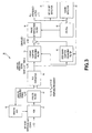
- a signal processing apparatus 100 of the configuration as shown in FIG. 1 is generally used.
- the signal processing apparatus 100 shown in FIG. 1 is an apparatus example in which digital adaptive equalizing filter is mounted (connected) at the succeeding stage of PLL for analog Voltage Controlled Oscillator (VCO) base magnetic recording which is generally used.
- a head reproduction signal x(t) having no non-linear distortion is equalized by an analog filter 101, and is converted into a digital signal by an A/D converter 102.
- This digital signal is delivered to a digital adaptive equalizing filter 103 and a phase error calculator 105.
- the digital adaptive equalizing filter 103 determines residual equalizing error between the digital signal and an ideal equalized signal by using detection data obtained from a Viterbi detector 111 to finally correct adaptive equalizing filter tap coefficients by using this residual equalizing error.
- a signal to which only equalization by analog filter has been performed is delivered to a PLL circuit 104, wherein a linearly adaptively equalized signal is not delivered thereto.
- the PLL circuit 104 is composed of a phase error calculator 105, a loop filter 106, a D/A converter 107, and a Voltage Controlled Oscillator (VCO) 108.
- the phase error calculator 105 calculates a phase error of a signal which has been analog-equalized by the analog filter 101 and has been then digitized by the D/A converter 107.
- the loop filter 106 outputs proportional term, differential term and integral term thereof by using suitable filter coefficients with respect to the phase error.
- the D/A converter 107 converts integral value of the phase error into an analog signal.
- the VCO 108 generates sampling clock fs for correcting phase from phase error signal converted into analog signal by using channel frequency fch from a frequency synthesizer 109 to deliver the sampling clock fs to the A/D converter 102. Further, the A/D converter 102 adjusts phase of a filter output signal of the analog filter 101 by using the sampling clock fs.
- adaptive equalizing filter is mounted (connected) at the succeeding stage of PLL device as in the case of the above-mentioned example.
- adaptive equalizing filter is mounted (connected) at the preceding stage of PLL to perform, as PLL operation, phase synchronization by PLL by using data having less distortion which has been compared with equalized ideal waveform.
- phase locked loop for processing digital signal of the Interpolated Timing Recovery (ITR) system is put into practical use.
- ITR Interpolated Timing Recovery
- a signal processing apparatus 120 of the representative configuration in which digital adaptive equalizing filter is provided at the preceding stage of an ITR-PLL 125 for magnetic recording/reproduction signal is shown in FIG. 2.
- a head reproduction signal x(t) having no non-linearity is inputted to an analog filter 121, at which anti-aliasing thereof is performed.
- the head reproduction signal which has been caused to undergo anti-aliasing is inputted to an A/D converter 122.
- the digital adaptive equalizing filter 123 equalizes the head reproduction signal x(k) by a desired equalization system, e.g., partial response classes I, II, IV and extended partial responses thereof, etc.
- a desired equalization system e.g., partial response classes I, II, IV and extended partial responses thereof, etc.
- excess signal taking place by difference between channel frequency and sampling frequency is produced in principle. This signal is regarded as the point where mismatching of signal takes place, i.e., the point where jump of phase takes place. At later time, such signal is predicted and is thinned at data detector, thereby making it possible to obtain only necessary signal.
- various methods are proposed for interpolation of sampling data at a digital PLL 125 using ITR system.
- phase is interpolated by FIR filter
- tap coefficients thereof Sinc function, Sinc function multiplied by various window functions used in digital signal processing, and FIR filter tap coefficients obtained by inverse Fourier-transforming a filter having a predetermined frequency characteristic, etc.
- the configuration in which digital filter is provided at the preceding stage of the PLL for analog VCO base magnetic recording shown in FIG. 1 and the configuration in which adaptive equalizing filter is provided at the preceding stage of the ITR system PLL shown in FIG. 2 is different in dependency upon whether or not adaptive equalizing filter can be mounted (connected) at the preceding stage of the PLL.
- improvement in PLL performance is expected so that this configuration is employed in hard disc products, etc.
- non-linear distortion of an input signal exerts bad influence on the equalization characteristic of equalized signal and PLL characteristic thereof, etc. thus to deteriorate error rate characteristic of reproduction signal.
- influence on the PLL characteristic is taken into consideration, calculation error of PLL phase error deteriorates phase synchronization performance.
- phase synchronization function by PLL is broken or failed in dependency upon mechanical relative position error at the time of chucking and/or unevenness of the medium performance in the system where Signal to Noise Ratio (SNR) of reproduction signal obtained from magnetic reproduction head or photo-detector, etc. is low and/or data reproducing unit in which the medium is of the detachable type, and the reproduction condition of the reproducing unit.
- SNR Signal to Noise Ratio
- An object of the present invention is to provide a novel signal processing apparatus and a novel signal processing method which can solve problems that prior arts have.
- Another object of the present invention is to provide a signal processing apparatus and a signal processing method which are adapted for correcting non-linear distortion of reproduction signal to resultantly improve PLL performance to improve, followed by such improvement, equalizing characteristic to finally improve error rate of the entirety of the signal processing system.
- the signal processing apparatus further comprises: phase interpolation means for performing interpolation of phase on the basis of a filter output of the first adaptive equalizing filter means and a filter output of the second adaptive equalizing filter means; and phase locked loop means for synchronizing phase of the phase interpolation means on the basis of an interpolated output fed back from the phase interpolation means.
- the signal processing method comprises: an analog filter step for performing band limitation of a reproduction signal having non-linear distortion and for performing analog equalization thereof; a first adaptive equalizing filter step for equalizing a linear signal of a filter output of the analog filter step; and a second adaptive equalizing filter step executed in parallel to the first adaptive equalizing filter step in order to correct non-linear distortion that the filter output of the analog filter step has.
- the signal processing method may further comprise a phase interpolation step for performing interpolation of phase on the basis of a filter output of the first adaptive equalizing filter step and a filter output of the second adaptive equalizing filter step; and a phase locked loop step for synchronizing phase of the phase interpolation step on the basis of an interpolated output fed back from the phase interpolation step.
- This embodiment is directed to a reproduction signal processing apparatus 10 for magnetic recording which is adapted for processing MR head reproduction signal from hard disc drive using Magneto Resistive (MR) head.
- the reproduction processing apparatus 10 for magnetic recording is supplied with a reproduction signal r(t) of the MR head at time t.
- the magnetic field voltage conversion characteristic has non-linear response.
- the reproduction signal r(t) of the MR head has non-linear distortion because of non-linear response that the MR head has.
- the entire configuration of the reproduction signal processing apparatus 10 for magnetic recording will be explained.
- the reproduction signal r(t) is passed through a Variable Gain Amplifier (VGA) 11, and is delivered to an anti-aliasing filter 12.
- VGA Variable Gain Amplifier
- the anti-aliasing filter 12 implements band limitation and analog equalization to the reproduction signal which has been passed through the VGA 11.
- An analog filter output of the analog anti-aliasing filter 12 is delivered to an analog Auto Gain Control (AGC) circuit 13.
- AGC Auto Gain Control
- the analog AGC circuit 13 determines peak value of output waveform amplitude of the analog anti-aliasing filter 12 to calculate level error as error between the peak value thus determined and ideal detection value.
- the level error is delivered to analog integration filter within the analog AGC circuit 13, at which its error quantity is integrated.
- the error quantity which has been integrated at the analog integration filter is fed back to the VGA 11.
- the VGA 11 adjusts level of amplitude of the reproduction signal r(t).
- the analog filter output of the analog anti-aliasing filter 12, i.e., analog equalized signal x 0 (t) which is equalized signal is also delivered to an A/D converter 14.
- the A/D converter 14 performs sampling of the analog equalized signal x 0 (t) at a predetermined sampling frequency.
- a signal which has been undergone sampling at time k by the A/D converter 14 is assumed to be x 0 (k).
- the analog equalized signal x 0 (k) which has been undergo sampling at the time k is delivered to a primary adaptive equalizing filter 15 and a secondary adaptive equalizing filter 16.
- the primary adaptive equalizing filter 15 equalizes a linear signal of the analog equalized signal x 0 (k). Least Mean Square (LMS) algorithm, etc. is used.
- the primary adaptive equalizing filter 15 detects an error signal between target detection value in accordance with a predetermined equalization system and actually detected signal with respect to an input waveform having no non-linear distortion. Further, it is guaranteed as principle that convergence into such tap coefficients to minimize square of error signal is made.
- the secondary adaptive equalizing filter 16 is connected in parallel with the primary adaptive equalizing filter 15 for the purpose of correcting non-linear distortion that the analog equalized signal x 0 (k) has.
- the secondary adaptive equalizing filter 16 is a filter in which polynomial filter is applied, and is called Volterra filter.
- the Volterra filter can optimize tap coefficients thereof in accordance with the adaptive equalization theory such as LMS, etc.
- Filter outputs of the primary adaptive equalizing filter 15 and the secondary adaptive equalizing filter 16 are added at an adder 17, and the added output is delivered to a phase interpolation filter 18 as equalized output y(k).
- the phase interpolation filter 18 performs interpolation of phase on the basis of filter output which is sum of filter output of the primary adaptive equalizing filter 15 and filter output of the secondary adaptive equalizing filter 16.
- a filter output of the phase interpolation filter 18 is delivered to an ITR-PLL circuit 19. Further, PLL processed output z(k) from the phase interpolation filter 18 is guided (delivered) to the external, and is also delivered to a Viterbi detector 20 and a bit-by-bit detector 21. A detection result of the Viterbi detector 20 is fed back to the primary adaptive equalizing filter 15 and the secondary adaptive equalizing filter 16.
- the VGA 11 adjusts level of the reproduction signal r(t) in response to feedback of integral value of level error between peak value of waveform amplitude of the analog filter output that the analog AGC circuit 13 has determined and ideal detection value on the basis of filter output of the analog anti-aliazing filter 12.
- the analog anti-aliasing filter 12 there is used a filter in which 7 pole 2 zero filter is parameter-optimized for PR4 equalization.
- the analog AGC circuit 13 determines peak value of the waveform amplitude thereof from analog filter output of the analog anti-aliasing filter 12 to calculate error (level error) between the peak value thus determined and ideal detection value. Thereafter, its error quantity is integrated at analog integration filter. The error quantity thus integrated is fed back to the VGA 11 to thereby adjust the amplitude so that the A/D converter 14 has an input of a suitable level.
- the primary adaptive equalizing filter 15 and the secondary adaptive equalizing filter 16 can be represented as respective terms of the following formula (1).
- the right side first term of the formula (1) indicates the primary adaptive equalizing filter and the right side second term indicates the secondary adaptive equalizing filter.
- x(k) is an input signal sampled at time k
- y(k) is sum of outputs of the primary and secondary adaptive equalizing filters.
- M1 is tap length of the primary adaptive equalizing filter 15
- M2 is tap length of the secondary adaptive equalizing filter 16, wherein respective filters have M2 ⁇ M2 number of secondary taps in practice.
- ⁇ (1) is step size parameter of the primary adaptive equalizing filter 15.
- h(2) (k, i1, i2) is updating tap coefficients at time k of the secondary adaptive equalizing filter 16, and updating relation by LMS algorithm thereof is represented by the following formula (4).
- h (2) (k+1,i 1 ,i 2 ) h (2) (k,i 1 ,i 2 ) + ⁇ (2) e(k) ⁇ x(k-i 1 ) ⁇ x(k-i 2 )
- ⁇ (2) is step size parameter of the secondary adaptive equalizing filter 16.
- phase interpolation filter 18 At the phase interpolation filter 18, a desired phase shift is implemented so that phase synchronization is taken.
- various methods are proposed for interpolation of sampling data at the digital PLL 19 using the ITR system.
- the tap length of the phase interpolation filter 18 is set to 10 taps.
- tap coefficients of the phase interpolation filter 18 there is used Sinc function having null points every channel period Tch on the time axis, and resolution of phase is set to (Tch/128).
- phase is interpolated by the FIR filter
- tap coefficients thereof Sinc function multiplied by various window functions used in digital signal processing, and/or FIR filter tap coefficients obtained by performing inverse Fourier transform of filter having a predetermined frequency characteristic, etc. in addition to the fact that Sinc function is used.
- the digital PLL of the ITR system is already known technology, and the configuration thereof is described in detail in the previously mentioned literature " A MMSE Interpolated Timing Recovery Scheme for The Magnetic Recording Channel, Zi-Ning Wu, John M. Cioffi, et al., Communications, 1997. ICC '97 Montreal, Towards the Knowledge Millennium, 1997 IEEE International Conference on, Volume:3, 1997 pp 1625-1629 vol. 3", and the literature "Interpolated Timing Recovery for Hard Disk Drive Read Channels, Mark Spurbeck, Richard T. Behrens, Communications, 1997. ICC '97 Montreal, Towards the Knowledge Millennium. 1997 IEEE International Conference on, Volume:3, 1997 pp 1618-1624 vol. 3".
- the adaptive equalizing filter linearly interpolates detection point error thereof by the theory of Inverse ITR described in these literatures to thereby deliver an interpolated output thus obtained to adaptive equalizing filter asynchronous to channel frequency of the preceding stage.
- the above-described primary and secondary adaptive equalizing filters substitute adaptive equalizing filter unit of the conventional ITR system PLL device and operate as primary and secondary adaptive equalizing filters which are asynchronous to channel frequency.
- the Viterbi detector 20 is, e.g., Viterbi detector for PR4, and serves to detect error rate of adaptively equalized PLL output at time k.
- the bit-by-bit detector 21 also detects error rate of adaptively equalized PLL output at time k.
- MR head reproduction waveform having non-linear distortion which is inputted to the reproduction signal processing apparatus for magnetic recording is determined by modeling.
- pw is half-value width of Lorentz waveform, and is a value obtained by dividing half-value width of isolated reproduction wave by period Tch of channel clock at a predetermined recording density. Such value is defined as Normalized Linear Density (NLD).
- NLD Normalized Linear Density
- A is peak amplitude of isolated reproduction wave in the magnetization reversal area represented by Lorentz waveform.
- a linear magnetic field inputted to the MR reproduction head was generated by convolution of the Lorentz waveform represented by the formula (1) and reproduction code pattern.
- the non-linear response of the MR head means that output voltage non-linearly responds to the input magnetic field.
- response curve of the MR head is of arctan type. Its input/output characteristic is shown in FIG. 4.
- ⁇ x is parameter indicating bias point, wherein offset produced thereby is corrected by the second term.
- parameter indicating non-linearity of reproduction signal is defined.
- Asymmetry model of MR head reproduction waveform is shown in FIG. 5.
- crest (peak) value of positive reproduction voltage is ⁇
- crest (peak) value of negative reproduction waveform is ⁇ in isolated reproduction waveform
- asymmetry ratio R is defined by the following formula (7).
- ⁇ and ⁇ are represented by the following formulas (8) and (9).
- ⁇
- ⁇
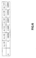
- bias point parameter ⁇ x and asymmetry ratio R have the relationship shown in FIG. 6. It is to be noted that normalized linear density is assumed to be 2.25 and respective magnetization reversal areas are sufficiently apart.
- average crest (peak) value of isolated reproduction wave having asymmetry is caused to be 1.0 to thereby determine magnitude of Additive White Gaussian Noise (AWGN).
- Amplitude correction gain GMR after outputted from the MR head is set to a value such that average crest (peak) value is equal to 1.0, i.e., the formula (11) indicated below.
- G MR 2 ⁇ + ⁇
- the amplitude correction gain GMR is used so that average amplitude of isolated reproduction waveform having asymmetry becomes equal to 1.0.
- signal amplitude of the isolated reproduction waveform can be regarded as 1.0.
- Magnitude of variance of AWGN is determined under such assumption so that suitable input SNR is provided to perform addition thereof.
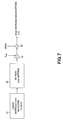
- FIG. 7 The configuration diagram of generation block of MR head reproduction waveform x(t) caused to have non-linearity of the arctan type which has been explained is shown in FIG. 7.
- a linear reproduction waveform generating unit 31 generates Lorentz waveform of the formula (5).
- a MR head non-linear mapping unit 32 performs transformation of head reproduction waveform by non-linear mapping of the arctan type in accordance with the transform relation of the formula (6).
- a multiplication unit 33 multiplies transform output of the MR head non-linear mapping unit 32 by amplitude correction gain GMR after outputted from MR head in accordance with the formula (11). Further, an adding unit 34 determines magnitudes of variance of AWGN so that multiplication output of the multiplication unit 33 is caused to have suitable input SNR to add them. Thus, it is possible to generate MR head reproduction waveform x(t).
- training of taps of the adaptive equalizing filter is performed by random data 100,000 points to utilize the converged tap coefficients as initial value of tap. Further, in the state where the adaptive equalization operation is stopped, SDNR (Signal and Distortion to Noise Ratio), error rate (bit-by-bit detector), error rate (Viterbi detector for PR4), and phase error variance after adaptive equalization by random data 1,000,000 is performed are calculated. Parameter is input SNR of head reproduction signal. Codes used are DC free codes of 8/9 rate, and adaptive equalization was performed with partial response class IV (PR4) being as target. With respect to an input signal, when crest (peak) value of isolated reproduction wave is 1.0, asymmetry ratio R was set to 0.22.
- the case where the secondary adaptive equalizing filter operation is turned OFF is referred to as the condition (1)
- the case where the secondary adaptive equalizing filter operation is turned ON is referred to as the condition (2).
- the input SNR was changed within the range from 21 to 27 dB.
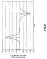
- Equalized eye pattern of the condition (1) is shown in FIG. 8
- equalized eye pattern of the condition (2) is shown in FIG. 9.
- SDNR 10 log 10 ( S 2 / ⁇ 2 )
- SDNR of the condition (2) is above SDNR of the condition (1) within all input SNR areas.
- phase error used in PLL As the calculation formula of phase error used in the first embodiment, there is used the formula (13) of timing gradient described in the literature "Roy D. Cideciyan, F. Dolivo, et at. A PRML System for Digital Magnetic Recording, IEEE Journal on Selected Areas in Communications, Volume: 10, NO. 1, January 1992. Pages(s) : 38-56".
- ⁇ (k) - z (k) ⁇ z(k-1) + z (k-1) ⁇ z(k)
- ⁇ (k) is calculation quantity of phase error at time k
- z(k) is adaptively equalized PLL output at time k
- z ⁇ (k) is bit-by-bit detection value (-1, 0, 1) of z(k) at time k.
- the second embodiment is directed to a reproduction signal processing apparatus 40 of FIG. 13 which is adapted for reproducing an optical disc of the phase change system having capacity corresponding to 27GB and diameter of 12 cm.
- asymmetry in upper and lower directions of reproduction signal conspicuously appears by the influence of radial skew.
- the reproduction signal processing apparatus of the second embodiment aims at removing asymmetry in upper and lower directions of reproduction signal taking place by radial skew of the optical disc of the phase change system.
- the phase change system optical disc is reproduced by an optical disc reproducing unit 41 shown in FIG. 13.
- the optical disc reproducing unit 41 comprises a spin stand for experiment, and is adapted to have ability to generate radial skew.
- anti-aliasing of reproduction signal is performed by analog filter.
- the reproduction signal thus obtained is delivered to an A/D converter 42 as reproduction signal x(t).
- the A/D converter 42 samples analog equalized signal x(t) sampled by a predetermined sampling frequency.
- a signal thus sampled at time k is assumed to be x 0 (k).
- the equalized signal x 0 (k) sampled at the time k is delivered to a primary adaptive equalizing filter 43 and a secondary adaptive equalizing filter 44.
- the equalized signal x 0 (k) is adaptively equalized into PR (1 2 2 1). Further, error rate was measured by the Viterbi detector 48. In this example, measurement of error rate by the Viterbi detector 48 was performed by the primary and secondary adaptive equalizing filters 43 and 44 after tap coefficients have been sufficiently converged.
- the signal processing apparatus serves to equalize linear signal of filter output of analog filter means by the first adaptive equalizing filter means to correct, by the second adaptive equalizing filter means connected in parallel with the first adaptive equalizing filter, non-linear distortion that filter output of the analog filter means has. Accordingly, it is possible to remove reproduction signal having non-linearity.
- the signal processing method comprises: equalizing linear signal of filter output of analog filter step at first adaptive equalizing filter step; and correcting, in parallel to the first adaptive equalizing filter step, non-linear distortion that filter output of analog filter step has at second adaptive equalizing filter step.
- first adaptive equalizing filter step equalizing linear signal of filter output of analog filter step at first adaptive equalizing filter step
- second adaptive equalizing filter step correcting, in parallel to the first adaptive equalizing filter step, non-linear distortion that filter output of analog filter step has at second adaptive equalizing filter step.
Landscapes
- Engineering & Computer Science (AREA)
- Signal Processing (AREA)
- Signal Processing For Digital Recording And Reproducing (AREA)
Applications Claiming Priority (3)
| Application Number | Priority Date | Filing Date | Title |
|---|---|---|---|
| JP2003148122 | 2003-05-26 | ||
| JP2003148122A JP2004348929A (ja) | 2003-05-26 | 2003-05-26 | 信号処理装置及び信号処理方法 |
| PCT/JP2004/007451 WO2004105025A1 (ja) | 2003-05-26 | 2004-05-25 | 信号処理装置及び信号処理方法 |
Publications (2)
| Publication Number | Publication Date |
|---|---|
| EP1511033A1 true EP1511033A1 (de) | 2005-03-02 |
| EP1511033A4 EP1511033A4 (de) | 2006-10-18 |
Family
ID=33475384
Family Applications (1)
| Application Number | Title | Priority Date | Filing Date |
|---|---|---|---|
| EP04734742A Withdrawn EP1511033A4 (de) | 2003-05-26 | 2004-05-25 | Apparat und methode zur signalübertragung |
Country Status (4)
| Country | Link |
|---|---|
| US (1) | US20050219727A1 (de) |
| EP (1) | EP1511033A4 (de) |
| JP (1) | JP2004348929A (de) |
| WO (1) | WO2004105025A1 (de) |
Cited By (1)
| Publication number | Priority date | Publication date | Assignee | Title |
|---|---|---|---|---|
| EP2337241A1 (de) * | 2009-12-18 | 2011-06-22 | Alcatel Lucent | Trägerphasenschätzer zur nichtlinearen Beeinträchtigungsüberwachung und -minderung in einem kohärenten optischen System |
Families Citing this family (18)
| Publication number | Priority date | Publication date | Assignee | Title |
|---|---|---|---|---|
| KR100614241B1 (ko) * | 2005-02-07 | 2006-08-21 | 삼성전자주식회사 | 적응형 등화기의 초기값 설정 방법 및 장치 |
| JP4696672B2 (ja) * | 2005-05-10 | 2011-06-08 | ソニー株式会社 | 位相同期装置および方法、データ再生装置および方法、並びに、プログラム |
| JP4581828B2 (ja) * | 2005-05-10 | 2010-11-17 | ソニー株式会社 | データ再生装置および方法、並びに、プログラム |
| JP4665597B2 (ja) * | 2005-05-10 | 2011-04-06 | ソニー株式会社 | 位相同期装置および方法、データ再生装置および方法、並びに、プログラム |
| US7236319B2 (en) * | 2005-06-08 | 2007-06-26 | Fujifilm Corporation | Reproducing method, reproducing apparatus, recording and reproducing apparatus, and magnetic recording medium |
| JP4945955B2 (ja) * | 2005-08-19 | 2012-06-06 | ソニー株式会社 | タップ係数設計方法及びタップ係数設計装置 |
| JP2008159138A (ja) * | 2006-12-22 | 2008-07-10 | Sony Corp | 再生装置および再生方法、信号処理装置および信号処理方法、並びにプログラム |
| JP5320567B2 (ja) * | 2007-03-29 | 2013-10-23 | 独立行政法人国立高等専門学校機構 | 光ディスク用再生等化方法および再生等化回路 |
| CN101320982B (zh) * | 2007-06-06 | 2011-12-07 | 智原科技股份有限公司 | 时序回复参数产生电路以及信号接收电路 |
| JP5249541B2 (ja) * | 2007-08-22 | 2013-07-31 | 株式会社モバイルテクノ | 伝搬路推定装置及び受信装置 |
| US7633704B2 (en) * | 2008-04-28 | 2009-12-15 | Seagate Technology Llc | Regulating tuning rate of adaptive filter coefficients for feed-forward disturbance rejection in a servo control loop |
| US8296638B2 (en) * | 2009-05-04 | 2012-10-23 | Seagate Technology Llc | Viterbi detector that associates multiple data dependent noise prediction filters with each possible bit pattern |
| US8611820B2 (en) * | 2009-09-22 | 2013-12-17 | Qualcomm Incorporated | Signal separation for energy harvesting |
| US20110069749A1 (en) * | 2009-09-24 | 2011-03-24 | Qualcomm Incorporated | Nonlinear equalizer to correct for memory effects of a transmitter |
| JP5445416B2 (ja) * | 2010-09-21 | 2014-03-19 | 株式会社Jvcケンウッド | 等化器および等化方法 |
| US8810949B2 (en) * | 2012-12-21 | 2014-08-19 | Lsi Corporation | Equalization combining outputs of multiple component filters |
| CN117957658B (zh) | 2021-01-11 | 2025-11-07 | Ysi公司 | 用于改进传感器线性度的引入串扰电路 |
| CN119299268B (zh) * | 2024-12-11 | 2025-04-18 | 欢领(上海)科技有限公司 | 自适应模拟均衡装置、系统和算法 |
Family Cites Families (10)
| Publication number | Priority date | Publication date | Assignee | Title |
|---|---|---|---|---|
| IT1118625B (it) * | 1979-05-11 | 1986-03-03 | Cselt Centro Studi Lab Telecom | Perfezionamenti agli equializzatori per trasmissione di segnali numeri ci |
| JP2001525101A (ja) * | 1998-02-12 | 2001-12-04 | コーニンクレッカ フィリップス エレクトロニクス エヌ ヴィ | 非線形尤逐次推定のための方法及び装置 |
| US6519715B1 (en) * | 1998-05-22 | 2003-02-11 | Hitachi, Ltd. | Signal processing apparatus and a data recording and reproducing apparatus including local memory processor |
| US7012772B1 (en) * | 1998-09-02 | 2006-03-14 | Cirrus Logic, Inc. | Sampled amplitude read channel employing an adaptive non-linear correction circuit for correcting non-linear distortions in a read signal |
| JP3486145B2 (ja) * | 2000-01-17 | 2004-01-13 | 松下電器産業株式会社 | デジタル記録データ再生装置 |
| JP2001344903A (ja) * | 2000-06-02 | 2001-12-14 | Hitachi Ltd | デジタル情報再生装置 |
| US7251297B2 (en) * | 2000-11-22 | 2007-07-31 | Broadcom Corporation | Method and system to identify and characterize nonlinearities in optical communications channels |
| US6678105B2 (en) * | 2001-05-17 | 2004-01-13 | International Business Machines Corporation | Nonlinear equalizer and decoding circuit and method using same |
| KR20030029654A (ko) * | 2001-06-19 | 2003-04-14 | 코닌클리케 필립스 일렉트로닉스 엔.브이. | 디지털 정보신호 재생장치 |
| US6788482B2 (en) * | 2001-06-29 | 2004-09-07 | Infineon Technologies Ag | Method and apparatus for Viterbi detector state metric re-normalization |
-
2003
- 2003-05-26 JP JP2003148122A patent/JP2004348929A/ja not_active Abandoned
-
2004
- 2004-05-25 WO PCT/JP2004/007451 patent/WO2004105025A1/ja not_active Ceased
- 2004-05-25 US US10/518,677 patent/US20050219727A1/en not_active Abandoned
- 2004-05-25 EP EP04734742A patent/EP1511033A4/de not_active Withdrawn
Cited By (5)
| Publication number | Priority date | Publication date | Assignee | Title |
|---|---|---|---|---|
| EP2337241A1 (de) * | 2009-12-18 | 2011-06-22 | Alcatel Lucent | Trägerphasenschätzer zur nichtlinearen Beeinträchtigungsüberwachung und -minderung in einem kohärenten optischen System |
| WO2011072980A1 (en) * | 2009-12-18 | 2011-06-23 | Alcatel Lucent | Carrier phase estimator for non-linear impairment monitoring and mitigation in coherent optical systems |
| CN102656824A (zh) * | 2009-12-18 | 2012-09-05 | 阿尔卡特朗讯 | 用于相干光系统中非线性损害监视和减轻的载波相位估计器 |
| CN102656824B (zh) * | 2009-12-18 | 2015-04-22 | 阿尔卡特朗讯 | 用于相干光系统中非线性损害监视和减轻的载波相位估计器 |
| US9166682B2 (en) | 2009-12-18 | 2015-10-20 | Alcatel Lucent | Carrier phase estimator for non-linear impairment monitoring and mitigation in coherent optical systems |
Also Published As
| Publication number | Publication date |
|---|---|
| JP2004348929A (ja) | 2004-12-09 |
| WO2004105025A1 (ja) | 2004-12-02 |
| US20050219727A1 (en) | 2005-10-06 |
| EP1511033A4 (de) | 2006-10-18 |
Similar Documents
| Publication | Publication Date | Title |
|---|---|---|
| US6449110B1 (en) | Optimizing operation of a disk storage system by increasing the gain of a non-linear transducer and correcting the non-linear distortions using a non-linear correction circuit | |
| EP1511033A1 (de) | Apparat und methode zur signalübertragung | |
| US7551668B2 (en) | Adaptive equalizing apparatus and method | |
| US7012772B1 (en) | Sampled amplitude read channel employing an adaptive non-linear correction circuit for correcting non-linear distortions in a read signal | |
| US6246723B1 (en) | Sampled amplitude read channel employing early-decisions from a trellis sequence detector for sampling value estimation | |
| US6208481B1 (en) | Gain and phase constrained adaptive equalizing filter in a sampled amplitude read channel for magnetic recording | |
| US6111710A (en) | Asynchronous/synchronous gain control for interpolated timing recovery in a sampled amplitude read channel | |
| US5572558A (en) | PID loop filter for timing recovery in a sampled amplitude read channel | |
| US6819514B1 (en) | Adaptive equalization and interpolated timing recovery in a sampled amplitude read channel for magnetic recording | |
| US5585975A (en) | Equalization for sample value estimation and sequence detection in a sampled amplitude read channel | |
| US6005731A (en) | Channel quality circuit employing a test pattern generator in a sampled amplitude read channel for calibration | |
| US5754353A (en) | Channel quality circuit in a sampled amplitude read channel | |
| US7440208B1 (en) | Flexible partial response targets for data detectors | |
| JP5054791B2 (ja) | Prml検出器 | |
| US6216249B1 (en) | Simplified branch metric for reducing the cost of a trellis sequence detector in a sampled amplitude read channel | |
| US5786951A (en) | Sampled amplitude read channel employing a discrete time noise generator for calibration | |
| JP2005276412A (ja) | 動的な等化器最適化を行うための装置 | |
| KR20020006683A (ko) | 디지털 기록 데이터 재생 장치 | |
| US5987634A (en) | Channel quality circuit in a sampled amplitude read channel | |
| US7545862B2 (en) | Adaptive equalizer, decoding device, and error detecting device | |
| CN100359591C (zh) | 盘装置和盘再现方法 | |
| US20030151838A1 (en) | Data decoding method and circuit and information recording and reproducing apparatus using the same | |
| CN100435231C (zh) | 自适应均衡电路和自适应均衡方法 | |
| KR20030029654A (ko) | 디지털 정보신호 재생장치 | |
| US7221638B2 (en) | Electronic circuit for decoding a read signal from an optical storage medium |
Legal Events
| Date | Code | Title | Description |
|---|---|---|---|
| PUAI | Public reference made under article 153(3) epc to a published international application that has entered the european phase |
Free format text: ORIGINAL CODE: 0009012 |
|
| 17P | Request for examination filed |
Effective date: 20041221 |
|
| AK | Designated contracting states |
Kind code of ref document: A1 Designated state(s): AT BE BG CH CY CZ DE DK EE ES FI FR GB GR HU IE IT LI LU MC NL PL PT RO SE SI SK TR |
|
| AX | Request for extension of the european patent |
Extension state: AL HR LT LV MK |
|
| RIC1 | Information provided on ipc code assigned before grant |
Ipc: G11B 20/22 20060101ALI20060130BHEP Ipc: G11B 20/18 20060101ALI20060130BHEP Ipc: G11B 20/10 20060101ALI20060130BHEP Ipc: G11B 20/14 20060101AFI20041209BHEP |
|
| A4 | Supplementary search report drawn up and despatched |
Effective date: 20060222 |
|
| DAX | Request for extension of the european patent (deleted) | ||
| RBV | Designated contracting states (corrected) |
Designated state(s): DE FR GB |
|
| RA4 | Supplementary search report drawn up and despatched (corrected) |
Effective date: 20060808 |
|
| RA4 | Supplementary search report drawn up and despatched (corrected) |
Effective date: 20060222 |
|
| 17Q | First examination report despatched |
Effective date: 20071105 |
|
| STAA | Information on the status of an ep patent application or granted ep patent |
Free format text: STATUS: THE APPLICATION IS DEEMED TO BE WITHDRAWN |
|
| 18D | Application deemed to be withdrawn |
Effective date: 20071203 |