EP1510889A2 - Bildanzeigegerät für dreidimensionale Hologramme - Google Patents
Bildanzeigegerät für dreidimensionale Hologramme Download PDFInfo
- Publication number
- EP1510889A2 EP1510889A2 EP04020200A EP04020200A EP1510889A2 EP 1510889 A2 EP1510889 A2 EP 1510889A2 EP 04020200 A EP04020200 A EP 04020200A EP 04020200 A EP04020200 A EP 04020200A EP 1510889 A2 EP1510889 A2 EP 1510889A2
- Authority
- EP
- European Patent Office
- Prior art keywords
- interference fringe
- hologram image
- image display
- electric field
- fringe patterns
- Prior art date
- Legal status (The legal status is an assumption and is not a legal conclusion. Google has not performed a legal analysis and makes no representation as to the accuracy of the status listed.)
- Granted
Links
Images




Classifications
-
- G—PHYSICS
- G02—OPTICS
- G02F—OPTICAL DEVICES OR ARRANGEMENTS FOR THE CONTROL OF LIGHT BY MODIFICATION OF THE OPTICAL PROPERTIES OF THE MEDIA OF THE ELEMENTS INVOLVED THEREIN; NON-LINEAR OPTICS; FREQUENCY-CHANGING OF LIGHT; OPTICAL LOGIC ELEMENTS; OPTICAL ANALOGUE/DIGITAL CONVERTERS
- G02F1/00—Devices or arrangements for the control of the intensity, colour, phase, polarisation or direction of light arriving from an independent light source, e.g. switching, gating or modulating; Non-linear optics
- G02F1/01—Devices or arrangements for the control of the intensity, colour, phase, polarisation or direction of light arriving from an independent light source, e.g. switching, gating or modulating; Non-linear optics for the control of the intensity, phase, polarisation or colour
- G02F1/13—Devices or arrangements for the control of the intensity, colour, phase, polarisation or direction of light arriving from an independent light source, e.g. switching, gating or modulating; Non-linear optics for the control of the intensity, phase, polarisation or colour based on liquid crystals, e.g. single liquid crystal display cells
-
- G—PHYSICS
- G03—PHOTOGRAPHY; CINEMATOGRAPHY; ANALOGOUS TECHNIQUES USING WAVES OTHER THAN OPTICAL WAVES; ELECTROGRAPHY; HOLOGRAPHY
- G03H—HOLOGRAPHIC PROCESSES OR APPARATUS
- G03H1/00—Holographic processes or apparatus using light, infrared or ultraviolet waves for obtaining holograms or for obtaining an image from them; Details peculiar thereto
- G03H1/02—Details of features involved during the holographic process; Replication of holograms without interference recording
-
- G—PHYSICS
- G03—PHOTOGRAPHY; CINEMATOGRAPHY; ANALOGOUS TECHNIQUES USING WAVES OTHER THAN OPTICAL WAVES; ELECTROGRAPHY; HOLOGRAPHY
- G03H—HOLOGRAPHIC PROCESSES OR APPARATUS
- G03H1/00—Holographic processes or apparatus using light, infrared or ultraviolet waves for obtaining holograms or for obtaining an image from them; Details peculiar thereto
- G03H1/04—Processes or apparatus for producing holograms
-
- G—PHYSICS
- G03—PHOTOGRAPHY; CINEMATOGRAPHY; ANALOGOUS TECHNIQUES USING WAVES OTHER THAN OPTICAL WAVES; ELECTROGRAPHY; HOLOGRAPHY
- G03H—HOLOGRAPHIC PROCESSES OR APPARATUS
- G03H1/00—Holographic processes or apparatus using light, infrared or ultraviolet waves for obtaining holograms or for obtaining an image from them; Details peculiar thereto
- G03H1/22—Processes or apparatus for obtaining an optical image from holograms
- G03H1/2294—Addressing the hologram to an active spatial light modulator
-
- G—PHYSICS
- G03—PHOTOGRAPHY; CINEMATOGRAPHY; ANALOGOUS TECHNIQUES USING WAVES OTHER THAN OPTICAL WAVES; ELECTROGRAPHY; HOLOGRAPHY
- G03H—HOLOGRAPHIC PROCESSES OR APPARATUS
- G03H1/00—Holographic processes or apparatus using light, infrared or ultraviolet waves for obtaining holograms or for obtaining an image from them; Details peculiar thereto
- G03H1/02—Details of features involved during the holographic process; Replication of holograms without interference recording
- G03H2001/0208—Individual components other than the hologram
- G03H2001/0224—Active addressable light modulator, i.e. Spatial Light Modulator [SLM]
-
- G—PHYSICS
- G03—PHOTOGRAPHY; CINEMATOGRAPHY; ANALOGOUS TECHNIQUES USING WAVES OTHER THAN OPTICAL WAVES; ELECTROGRAPHY; HOLOGRAPHY
- G03H—HOLOGRAPHIC PROCESSES OR APPARATUS
- G03H1/00—Holographic processes or apparatus using light, infrared or ultraviolet waves for obtaining holograms or for obtaining an image from them; Details peculiar thereto
- G03H1/02—Details of features involved during the holographic process; Replication of holograms without interference recording
- G03H2001/026—Recording materials or recording processes
- G03H2001/0268—Inorganic recording material, e.g. photorefractive crystal [PRC]
-
- G—PHYSICS
- G03—PHOTOGRAPHY; CINEMATOGRAPHY; ANALOGOUS TECHNIQUES USING WAVES OTHER THAN OPTICAL WAVES; ELECTROGRAPHY; HOLOGRAPHY
- G03H—HOLOGRAPHIC PROCESSES OR APPARATUS
- G03H1/00—Holographic processes or apparatus using light, infrared or ultraviolet waves for obtaining holograms or for obtaining an image from them; Details peculiar thereto
- G03H1/22—Processes or apparatus for obtaining an optical image from holograms
- G03H1/2202—Reconstruction geometries or arrangements
- G03H2001/2236—Details of the viewing window
- G03H2001/2239—Enlarging the viewing window
-
- G—PHYSICS
- G03—PHOTOGRAPHY; CINEMATOGRAPHY; ANALOGOUS TECHNIQUES USING WAVES OTHER THAN OPTICAL WAVES; ELECTROGRAPHY; HOLOGRAPHY
- G03H—HOLOGRAPHIC PROCESSES OR APPARATUS
- G03H2225/00—Active addressable light modulator
- G03H2225/20—Nature, e.g. e-beam addressed
- G03H2225/22—Electrically addressed SLM [EA-SLM]
-
- G—PHYSICS
- G03—PHOTOGRAPHY; CINEMATOGRAPHY; ANALOGOUS TECHNIQUES USING WAVES OTHER THAN OPTICAL WAVES; ELECTROGRAPHY; HOLOGRAPHY
- G03H—HOLOGRAPHIC PROCESSES OR APPARATUS
- G03H2225/00—Active addressable light modulator
- G03H2225/30—Modulation
- G03H2225/32—Phase only
-
- G—PHYSICS
- G03—PHOTOGRAPHY; CINEMATOGRAPHY; ANALOGOUS TECHNIQUES USING WAVES OTHER THAN OPTICAL WAVES; ELECTROGRAPHY; HOLOGRAPHY
- G03H—HOLOGRAPHIC PROCESSES OR APPARATUS
- G03H2225/00—Active addressable light modulator
- G03H2225/52—Reflective modulator
-
- G—PHYSICS
- G03—PHOTOGRAPHY; CINEMATOGRAPHY; ANALOGOUS TECHNIQUES USING WAVES OTHER THAN OPTICAL WAVES; ELECTROGRAPHY; HOLOGRAPHY
- G03H—HOLOGRAPHIC PROCESSES OR APPARATUS
- G03H2226/00—Electro-optic or electronic components relating to digital holography
- G03H2226/04—Transmission or communication means, e.g. internet protocol
-
- G—PHYSICS
- G03—PHOTOGRAPHY; CINEMATOGRAPHY; ANALOGOUS TECHNIQUES USING WAVES OTHER THAN OPTICAL WAVES; ELECTROGRAPHY; HOLOGRAPHY
- G03H—HOLOGRAPHIC PROCESSES OR APPARATUS
- G03H2227/00—Mechanical components or mechanical aspects not otherwise provided for
- G03H2227/02—Handheld portable device, e.g. holographic camera, mobile holographic display
-
- G—PHYSICS
- G03—PHOTOGRAPHY; CINEMATOGRAPHY; ANALOGOUS TECHNIQUES USING WAVES OTHER THAN OPTICAL WAVES; ELECTROGRAPHY; HOLOGRAPHY
- G03H—HOLOGRAPHIC PROCESSES OR APPARATUS
- G03H2240/00—Hologram nature or properties
- G03H2240/20—Details of physical variations exhibited in the hologram
- G03H2240/40—Dynamic of the variations
- G03H2240/42—Discrete level
-
- G—PHYSICS
- G03—PHOTOGRAPHY; CINEMATOGRAPHY; ANALOGOUS TECHNIQUES USING WAVES OTHER THAN OPTICAL WAVES; ELECTROGRAPHY; HOLOGRAPHY
- G03H—HOLOGRAPHIC PROCESSES OR APPARATUS
- G03H2240/00—Hologram nature or properties
- G03H2240/50—Parameters or numerical values associated with holography, e.g. peel strength
- G03H2240/61—SLM related parameters, e.g. pixel size
Definitions
- the present invention relates to a three-dimensional hologram image display apparatus and a three-dimensional hologram image display system, each of which displays a three-dimensional hologram image by use of computed interference fringe patterns (computer generated hologram).
- a three-dimensional hologram image display apparatus which irradiates a reference wave onto a computer generated hologram displayed (played back) on a liquid crystal display (LCD) so as to reproduce an object wave, thus displaying a three-dimensional hologram image.
- the computer generated hologram consists of interference fringe patterns obtained by a computation.
- interference fringe patterns are created from the object wave and the reference wave.
- the object wave is created in a manner that a laser beam irradiated onto an object of a three-dimensional shape is reflected thereon.
- resolution of 1 ⁇ m or less is required for displaying the three-dimensional hologram image of the object of the three-dimensional shape.
- resolution of approximately 10 ⁇ m is required for displaying the three-dimensional hologram image of the object of the three-dimensional shape.
- the conventional three-dimensional hologram image display apparatus does not have the sufficient resolution for displaying the three-dimensional hologram image of the object of the three-dimensional shape.
- the conventional three-dimensional hologram image display apparatus has had a problem in that the three-dimensional hologram image of the object of the three-dimensional shape can be observed only by use of a peephole system having a narrow field of view.
- a three-dimensional hologram image display system using photorefractive crystal has been known as a system which supplement limitations of the resolution of the LCD (restrictions of the field of view).
- the three-dimensional hologram image display system is configured with an interference fringe pattern computing apparatus 1, an interference fringe pattern recording apparatus 2a, reference wave irradiation apparatuses 3a and 3b, and an interference fringe pattern display apparatus 4.
- the interference fringe pattern computing apparatus 1 is configured with a computer 11. As shown in FIG. 1, the interference fringe pattern computing apparatus 1 is configured to compute the interference fringe patterns (computer generated hologram) created from the object wave and the reference wave.
- the interference fringe pattern display apparatus 4 is configured with an electronic display device (LCD 12 in an example of FIG. 2).
- the interference fringe pattern display apparatus 4 is configured to display an image of the interference fringe patterns computed by the interference fringe pattern computing apparatus 1.
- Information for displaying such an image of the interference fringe patterns is transmitted from the interference fringe pattern computing apparatus 1 to the interference fringe pattern display apparatus 4 by an image signal.
- the reference wave irradiation apparatus 3a is configured to irradiate a reference wave B1 toward the interference fringe pattern display apparatus 4 (LCD 12), and the reference wave irradiation apparatus 3b is configured to irradiate a reference wave B2 toward the interference fringe pattern recording apparatus 2a (hologram recording device 21).
- the reference wave B1 has the same wavelength and incidence angle as those of the reference wave for use in the computation of the interference fringe patterns by the interference fringe pattern computing apparatus 1.
- the object wave A1 has a beam wavefront equivalent to that of the object wave for use in the computation of the interference fringe patterns by the interference fringe pattern computing apparatus 1.
- the object wave A1 propagates to the interference fringe pattern recording apparatus 2a.
- the interference fringe pattern recording apparatus 2a is configured with the hologram recording device (light modulation device) 21.
- the interference fringe pattern recording apparatus 2a is configured to record an interference fringe patterns created from the object wave A1 and the reference wave B2 irradiated from the reference wave irradiation apparatus 3a, in the hologram recording device 21.
- the hologram recording device 21 the photorefractive crystal is used.
- the interference fringe patterns are recorded in the hologram recording device 21 (photorefractive crystal) as described above, when the object wave A1 from the interference fringe pattern display apparatus 4 is blocked by a shutter or the like, and only the reference wave B2 is irradiated toward the interference fringe pattern recording apparatus 2a, an object wave A2 is generated by the interference fringe patterns recorded in the hologram recording device 21.
- the observer can three-dimensionally observe the above-mentioned image of the three-dimensional shape by means of the object wave A2.
- Such a three-dimensional hologram image display system using the photorefractive crystal as the hologram recording device 21 rerecords the interference fringe patterns created from the object wave A1 played back by the LCD and from the reference wave B2, thus making it possible to achieve an enlargement of the field of view.
- the conventional three-dimensional hologram image display system using the photorefractive crystal is configured to record the interference fringe patterns in the interference fringe pattern recording apparatus 2a by use of an optical technique.
- the conventional three-dimensional hologram image display system has had a problem in that the conventional three-dimensional hologram image display system is difficult to downsize.
- a first aspect of the present invention is summarized as a three-dimensional hologram image display apparatus which displays a three-dimensional hologram image by use of computed interference fringe patterns.
- the three-dimensional hologram image display apparatus includes a light modulation device which has an electro-optical effect in which a refractive index is varied in accordance with an applied electric field intensity; and an electric field controller configured to record computed interference fringe patterns in the light modulation device by varying an electric field intensity applied to the light modulation device in accordance with the computed interference fringe patterns.
- pixel electrodes corresponding to respective pixels of the interference fringe patterns can be provided on a surface of the light modulation device.
- the electric field controller can be configured to vary the electric field intensity applied to the light modulation device by controlling voltages applied to the respective pixel electrodes.
- the electric field controller can be configured to store gray-scale values and voltage values of the interference fringe patterns in association with each other. And the electric field controller can be configured to apply voltages of the voltage values associated with the gray-scale values of the respective pixels in the interference fringe patterns, to the pixel electrodes corresponding to the respective pixels.
- the electric field controller can be configured to control the voltages applied to the respective pixel electrodes, in consideration of mutual functions of electric field intensities in adjacent pixels.
- the electric field controller can be configured to apply voltage only to a specific pixel electrode.
- the electric field controller can be configured not to apply voltages to pixel electrodes adjacent to a specific pixel electrode, when voltage applied to the specific pixel electrode is greater than or equal to a predetermined voltage.
- a second aspect of the present invention is summarized as a three-dimensional hologram image display system, which includes a three-dimensional hologram image display apparatus and a server, and displays a three-dimensional hologram image.
- the server includes an interference fringe pattern computer configured to compute interference fringe patterns created from an object wave and a reference wave; a storage configured to store gray-scale values and voltage values of the interference fringe patterns in association with each other; and a transmitter configured to transmit the voltage values associated with the gray-scale values of respective pixels in computed interference fringe patterns to the three-dimensional hologram image display apparatus.
- the three-dimensional hologram image display apparatus includes a light modulation device which has pixel electrodes corresponding to the respective pixels of the interference fringe patterns provided on a surface thereof, and has an electro-optical effect in which a refractive index is varied in accordance with an applied electric field intensity; and an electric field controller configured to record the interference fringe patterns in the light modulation device by applying, to pixel electrodes corresponding to the respective pixels, voltages of the voltage values associated with the gray-scale values of the respective pixels in the interference fringe patterns received from the server.
- FIG. 3 is a view showing an entire configuration of a three-dimensional hologram image display system in a first embodiment of the present invention.
- the three-dimensional hologram image display system is a three-dimensional hologram image display system which displays a three-dimensional hologram image by use of a computer generated hologram.
- the three-dimensional hologram image display system is configured with an interference fringe pattern computing apparatus 1, a three-dimensional hologram image display apparatus 2, and a reference wave irradiation apparatus 3.
- a concept of an "image” includes a still-frame picture, a moving picture (video).
- the interference fringe pattern computing apparatus 1 is configured with a computer.
- the interference fringe pattern computing apparatus 1 is configured to compute interference fringe patterns created from an object wave and a reference wave.
- the object wave is created in a manner that a laser beam irradiated onto an object of a three-dimensional shape (for example, 3D data of a cube) is reflected thereon.
- the interference fringe patterns are gray-scale images in which variations of brightness correspond to amplitude information of light and a fringe pattern corresponds to phase information of the light.
- the three-dimensional hologram image display apparatus 2 includes a light modulation device 25 in which a refractive index is varied in accordance with an electric field intensity.
- the three-dimensional hologram image display apparatus 2 is configured to record the interference fringe patterns in the light modulation device 25, by varying the electric field intensity applied to the light modulation device 25 in accordance with the interference fringe patterns.
- the three-dimensional hologram image display apparatus 2 is configured with a hologram recording device 21 and an electric field control unit 22.
- the hologram recording device 21 adopts a configuration in which electrodes 23 corresponding to the respective pixels of the interference fringe patterns are provided on a surface of the light modulation device 25 having the refractive index varied in accordance with an applied electric field intensity.
- the hologram recording device 21 adopts a configuration in which the light modulation device 25 is sandwiched between microelectrodes 23 and 24.
- the hologram recording device 21 may have an electrode structure of a simple matrix system.
- the hologram recording device 21 adopts a configuration in which the electrodes 23 in an X-axis direction are pasted on an upper surface of the light modulation device 25 formed as a thin film, and the electrodes 24 in a Y-axis direction are pasted on a lower surface of the light modulation device 25 formed as the thin film.
- intersection portions of the electrodes 23 in the X-axis direction and the electrodes 24 in the Y-axis direction apply to pixel electrodes 23a corresponding to the respective pixels.
- the hologram recording device 21 may have an electrode structure of an active matrix system.
- the hologram recording device 21 adopts a configuration in which transistors capable of independently controlling ON/OFF of each of the pixel electrodes 23a corresponding to the respective pixels are prepared.
- the light modulation device 25 used is a material such as PLZT, SBT and SBN which are ferroelectric materials capable of easily realizing refractive-index modulation by electric-field control by use of polarization inversion.
- the electric field control unit 22 is configured to vary the refractive index inside of the light modulation device 25, by varying the electric field intensity applied to the light modulation device 25, based on information for displaying the interference fringe patterns (gray-scale values of the respective pixels of the interference fringe patterns).
- the information is transmitted from the interference fringe pattern computing apparatus 1 by an image signal.
- FIG. 6A shows a part of the pixels (A, B, C%) constituting the interference fringe patterns computed by the interference fringe pattern computing apparatus 1.
- the electric filed control unit 22 applies voltages (A, B, C-.) shown in a bar graph of FIG. 6B to the respective pixel electrodes 23a corresponding to the respective pixels (A, B. C%) of the interference fringe patterns.
- the electric field control unit 22 can control the voltages applied to the respective pixel electrodes 23a completely independently.
- the electric field control unit 22 is configured to locally vary the refractive index inside of the light modulation device 25, by locally varying the electric field intensity applied to the light modulation device 25, so as to record the interference fringe patterns concerned in the light modulation device 25.
- the refractive index is constant in a state where an electric field intensity is not varied inside of the light modulation device 25.
- the electric field control unit 22 is configured to store the gray-scale values and voltage values of the interference fringe patterns in association with each other.
- the electric field control unit 22 may be configured to apply voltages of the voltage values associated with the gray-scale values of the respective pixels in the interference fringe patterns, to the pixel electrodes 23a corresponding to the respective pixels.
- the electric field control unit 22 computes and stores a relationship between the gray-scale values and voltage values of the interference fringe patterns for each material of the light modulation device 25 based on a relationship shown in FIG. 7B, which is between an applied electric field intensity and the refractive index inside of the light modulation device, a relationship between the gray-scale values of the interference fringe patterns and the refractive index inside of the light modulation device, and the like.
- the reference wave irradiation apparatus 3 is configured to irradiate a reference wave B toward the light modulation device 25.
- the reference wave B has the same wavelength and incidence angle as those of the reference wave for use in the computation of the interference fringe patterns by the interference fringe pattern computing apparatus 1.
- the same object wave A as light coming from the object of the three-dimensional shape for use in the computation of the interference fringe patterns by the interference fringe pattern computing apparatus 1 is made incident onto eyes of an observer, and thus the observer can three-dimensionally observe the above-described object of the three-dimensional shape.
- the three-dimensional hologram image display apparatus 2 according to the first embodiment is different from the three-dimensional hologram image display apparatus according to the prior art in that the variations of the refractive index of the hologram recording device 21 are controlled by the variations of the electric field intensity, that the recording of the interference fringe patterns in the hologram recording device 21 is realized not optically but electrically, and that the variations of the electric field intensity are realized by use of the polarization inversion.
- the interference fringe pattern computing apparatus 1 and the three-dimensional hologram image display apparatus 2 are provided as apparatuses separate from each other.
- the present invention is not limited to this configuration, and is also applicable to a configuration in which the three-dimensional hologram image display apparatus 2 includes a function of the interference fringe pattern computing apparatus 1.
- Step 401 the interference fringe pattern computing apparatus 1 computes the interference fringe patterns created from the object wave and the reference wave.
- the object wave is created in the manner that the laser beam irradiated onto the object of the three-dimensional shape is reflected thereon.
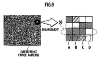
- FIG. 9 shows a state where the interference fringe patterns are displayed and a state where a local region of the displayed interference fringe patterns is enlarged.
- Each of squares "A” to "D” indicates one pixel constituting the interference fringe patterns.
- the interference fringe pattern computing apparatus 1 transmits the information for displaying the above-described interference fringe patterns, to the three-dimensional hologram image display apparatus 2 by the image signal.
- Step 403 as in a conventional liquid crystal display device and the like, the electric field control unit 22 of the three-dimensional hologram image display apparatus 2 controls the electric fields intensities applied to the respective pixel electrodes 23a corresponding to the respective pixels constituting the interference fringe patterns based on the gray-scale values of the respective pixels.
- FIG. 10 shows a cross-sectional view of the hologram recording device 21 of the three-dimensional hologram image display apparatus 2.
- pixel electrodes 23a (A) to 23a (D) correspond to the pixels "A" to "D", respectively.
- a relationship between the refractive index and the electric field intensity inside of the light modulation device 25 is the relationship shown in FIG. 7B.
- the electric field control unit 22 varies voltages applied to the pixel electrodes 23a (A) to 23a (D) to "+5V” “+4V” "+5V” and "+2V".
- the electric field control unit 22 applies the different voltages to the respective pixel electrodes 23a (A) to 23a (D) of the hologram recording device 21.
- Step S404 in the light modulation device 25, refractive-index modulations corresponding to the interference fringe patterns computed by the interference fringe pattern computing apparatus 1 are realized, and the interference fringe patterns concerned are recorded.
- FIG. 11 shows pixels "A” to "D” constituting the local region of the interference fringe patterns recorded in the light modulation device 25.
- refractive indices corresponding to the respective pixels "A" to “D” are shown by variations of shades of gray.
- Step 405 onto the light modulation device 25, the reference wave irradiation apparatus 3 irradiates the reference wave B having the same wavelength and incidence angle as those of the reference wave for use in the computation of the interference fringe patterns by the interference fringe pattern computing apparatus 1.
- Step 406 when the reference wave B is irradiated toward the light modulation device 25 in the state where the interference fringe patterns are recorded in the light modulation device 25, the object wave A is generated by the interference fringe patterns recorded in the light modulation device 25.
- the same object wave A as the light coming from the object of the three-dimensional shape for use in the computation of the interference fringe patterns by the interference fringe pattern computing apparatus 1 is made incident onto the eyes of the observer, and thus the observer can three-dimensionally observe the above-described object of the three-dimensional shape.
- the recording of the interference fringe patterns in the hologram recording device 25 can be controlled electrically. Accordingly, downsizing of the three-dimensional hologram image display system can be realized while realizing a three-dimensional hologram image display enabling a wide angle of view.
- the interference fringe pattern display apparatus 4 such as the LCD 12
- the interference fringe patterns created from the object wave A1 generated from the displayed interference fringe patterns and from the reference wave B2 is written into the hologram recording device.
- the downsizing of the three-dimensional hologram image display system can be realized.
- FIGS. 12A and 12B A three-dimensional hologram image display system according to a second embodiment of the present invention will be described with reference to FIGS. 12A and 12B.
- the interference fringe patterns are formed by synthesizing light waves, in the interference fringe patterns, the gray-scale values of the adjacent pixels are not radically varied as in the above-described image of the checker flag from a micro-level viewpoint.
- the interference fringe patterns to be played back are affected little in terms of deterioration.
- the electric field control unit 22 which plays back the interference fringe patterns can be configured to control the voltages applied to the respective pixel electrodes 23a (A) to 23a (D), in consideration of mutual functions of the electric field intensities applied to the adjacent pixel electrodes 23a (A) to 23a (D).
- the electric field control unit 22 it is not necessary for the electric field control unit 22 to control the pixel electrodes 23a corresponding to all of the pixels for each pair of the adjacent pixels completely independently.
- a state where the electric field intensity applied to the light modulation device 25 is controlled when the electric field control unit 22 cannot control the pixel electrodes corresponding to all of the pixels completely independently, that is, when electric fields applied to the adjacent pixel electrodes affect one another will be specifically described with reference to FIGS. 12A and 12B.
- FIG. 12A shows a part of the pixels (A, B, C%) constituting the interference fringe patterns computed by the interference fringe pattern computing apparatus 1.
- pixel electrodes adjacent to the pixel electrode 23a (C) corresponding to the pixel “C” may be only the pixel electrodes 23a (B) and 23a (D) corresponding to the pixels “B” and “D", or may include the pixel electrodes 23a (A) and 23a (E) corresponding to the pixels "A” and "E".
- the electric field control unit 22 lessens the voltages applied to the pixel electrodes 23a (A) and 23a (B) corresponding to the pixels "A" and “B” than true values, and increases the voltage applied to the pixel electrode 23a (C) corresponding to the pixel "C" more than a true value.
- the true values refer to the voltages applied to the respective pixel electrodes, when the electric field control unit 22 can control the pixel electrodes corresponding to all of the pixels completely independently (refer to FIG. 6B).
- the electric field control unit 22 can also thin out the pixel electrodes to which the voltages are applied in such a manner that the voltage applied to the pixel electrode corresponding to the pixel "C" is increased more than the true value and the voltages are not applied to the pixels "A", “B", “D”. "E” and the like, which are adjacent to the pixel "C”.
- the electric field control unit 22 does not have to control the voltages applied to the pixel electrodes corresponding to all of the pixels.
- the electric field control unit 22 can be configured to control only voltages applied to pixel electrodes corresponding to specific pixels.
- the electric field control unit 22 can obtain a similar result to that of "the gray-scale variation curve of the interference fringe patterns" shown in FIG. 6B, even if the electric field control unit 22 cannot control the pixel electrodes corresponding to all of the pixels completely independently, that is, even if the electric fields in the adjacent pixel electrodes affect one another.
- the electric field control unit 22 may also be configured not to apply the voltages to the pixel electrodes (for example, the pixels "A", “B", 'D' and "E") adjacent to the specific pixel electrode (for example, the pixel electrode corresponding to the pixel "C") when the voltage applied to the specific electrode is a predetermined voltage or more.
- a restriction condition that the adjacent electrodes must be controlled completely independently is relaxed, and accordingly, manufacture of the system becomes facilitated.
- FIGS. 13 to 15 A three-dimensional hologram image display system according to a third embodiment of the present invention will be described with reference to FIGS. 13 to 15.
- the three-dimensional hologram image display system includes a server 100, and a three-dimensional hologram image display apparatus 2.
- the three-dimensional hologram image display apparatus 2 is configured with a mobile communication terminal communicable with the server 100 through a packet communication network 5 will be described.
- the server 100 includes an interference fringe pattern computing unit 1a, a storage unit 1b, and a transmitter unit 1c.
- the interference fringe pattern computing unit 1a is configured to compute interference fringe patterns (computer generated hologram) created from an object wave and a reference wave.
- the storage unit 1b is configured to store gray-scale values and voltage values of the interference fringe patterns in association with each other.
- the transmitter unit 1c is configured to transmit voltage values associated with the gray-scale values of the respective pixels of the computed interference fringe patterns, to the three-dimensional hologram image display apparatus 2.
- the three-dimensional hologram image display apparatus 2 includes a communication unit 31, a hologram recording device 21, an electric field control unit 22, a light source 32, and a light reflecting plate 33.
- the communication unit 31 is configured to require the server 100 to transmit the voltage values corresponding to the gray-scale values of the respective pixels of the interference fringe patterns for displaying a three-dimensional hologram image, and to transmit the received voltage values to the electric field control unit 22.
- the electric field control unit 22 is configured to record the interference fringe patterns in the light modulation device 25 as the hologram recording device 21, by applying, to the pixel electrodes corresponding to the respective pixels, the voltages of the voltage values associated with the gray-scale values of the respective pixels of the interference fringe patterns.
- the gray-scale values of the respective pixels of the interference fringe patterns are received from the server 100 through the communication unit 31.
- a configuration of the hologram recording device 21 is similar to the configuration of the hologram recording device 21 according to the above-mentioned first embodiment.
- the light reflecting plate 33 is configured to create a reference wave B, by reflecting light from the light source 32.
- the reference wave B has the same wavelength and incidence angle as those of the reference wave for use in the computation of the interference fringe patterns by the interference fringe pattern computing unit 1a of the server 100.
- the light source 32 may be a backlight for use in a liquid crystal display of the mobile communication terminal, or may be a light source provided separately from such a backlight.
- the present invention is also applicable to a configuration in which the server 100 transmits the gray-scale values of the interference fringe patterns to the three-dimensional hologram image display apparatus 2 through the packet communication network 5.
- the three-dimensional hologram image display apparatus and the three-dimensional hologram image display system which realize the downsizing thereof while realizing the three-dimensional hologram image display enabling the wide angle of view, can be provided.
Landscapes
- Physics & Mathematics (AREA)
- General Physics & Mathematics (AREA)
- Nonlinear Science (AREA)
- Chemical & Material Sciences (AREA)
- Crystallography & Structural Chemistry (AREA)
- Optics & Photonics (AREA)
- Holo Graphy (AREA)
- Stereoscopic And Panoramic Photography (AREA)
- Testing, Inspecting, Measuring Of Stereoscopic Televisions And Televisions (AREA)
- Control Of Indicators Other Than Cathode Ray Tubes (AREA)
Applications Claiming Priority (4)
| Application Number | Priority Date | Filing Date | Title |
|---|---|---|---|
| JP2003208712 | 2003-08-25 | ||
| JP2003208712 | 2003-08-25 | ||
| JP2004216472 | 2004-07-23 | ||
| JP2004216472A JP4464751B2 (ja) | 2003-08-25 | 2004-07-23 | 立体画像表示装置及び立体画像表示システム |
Publications (3)
| Publication Number | Publication Date |
|---|---|
| EP1510889A2 true EP1510889A2 (de) | 2005-03-02 |
| EP1510889A3 EP1510889A3 (de) | 2005-09-14 |
| EP1510889B1 EP1510889B1 (de) | 2018-07-04 |
Family
ID=34106878
Family Applications (1)
| Application Number | Title | Priority Date | Filing Date |
|---|---|---|---|
| EP04020200.4A Expired - Lifetime EP1510889B1 (de) | 2003-08-25 | 2004-08-25 | Bildanzeigegerät für dreidimensionale Hologramme |
Country Status (5)
| Country | Link |
|---|---|
| US (1) | US7630110B2 (de) |
| EP (1) | EP1510889B1 (de) |
| JP (1) | JP4464751B2 (de) |
| KR (1) | KR100741151B1 (de) |
| CN (1) | CN100430841C (de) |
Cited By (1)
| Publication number | Priority date | Publication date | Assignee | Title |
|---|---|---|---|---|
| EP1662341A2 (de) * | 2004-11-26 | 2006-05-31 | NTT DoCoMo INC. | Bildanzeigevorrichtung und dreidimensionale Bildanzeigevorrichtung |
Families Citing this family (10)
| Publication number | Priority date | Publication date | Assignee | Title |
|---|---|---|---|---|
| KR100664872B1 (ko) * | 2005-04-11 | 2007-01-03 | 김영철 | 1차원 홀로그램을 이용한 영상 표시장치 |
| DE102006018689A1 (de) * | 2006-04-13 | 2007-10-25 | Seereal Technologies S.A. | Verfahren zum Rendern und Generieren computergenerierter Videohologramme in Echtzeit |
| US8588046B2 (en) * | 2006-09-07 | 2013-11-19 | Panasonic Corporation | Information recording device and information reproducing device |
| GB0709379D0 (en) * | 2007-05-16 | 2007-06-27 | Seereal Technologies Sa | Smart display extended |
| GB2446852B (en) * | 2007-02-12 | 2009-12-09 | Light Blue Optics Ltd | Data communication and processing system |
| GB0718659D0 (en) | 2007-05-16 | 2007-10-31 | Seereal Technologies Sa | Holograms |
| KR101993565B1 (ko) * | 2010-12-22 | 2019-06-26 | 시리얼 테크놀로지즈 에스.에이. | 관찰자 트래킹을 위한 조합된 광변조 장치 |
| JP5975318B2 (ja) * | 2011-11-30 | 2016-08-23 | 大日本印刷株式会社 | 表示装置 |
| KR102050503B1 (ko) * | 2012-10-16 | 2019-11-29 | 삼성전자주식회사 | 다수의 세그먼트로 분할된 광학적 어드레싱 공간 광변조기, 이를 이용한 홀로그래픽 3차원 영상 표시 장치 및 방법 |
| CN106338905B (zh) | 2016-10-31 | 2017-11-14 | 京东方科技集团股份有限公司 | 一种显示装置及其显示方法 |
Citations (3)
| Publication number | Priority date | Publication date | Assignee | Title |
|---|---|---|---|---|
| US3890035A (en) | 1971-09-17 | 1975-06-17 | Hitachi Ltd | Complex light spatial modulator |
| JP2003208712A (ja) | 2002-01-10 | 2003-07-25 | Fujitsu Ltd | 磁気パターン転写装置 |
| JP2004216472A (ja) | 2003-01-10 | 2004-08-05 | Emura Tekkosho:Kk | 野菜千切り機の拍子木切り及び千切り用送りロール |
Family Cites Families (11)
| Publication number | Priority date | Publication date | Assignee | Title |
|---|---|---|---|---|
| US5040225A (en) * | 1987-12-07 | 1991-08-13 | Gdp, Inc. | Image analysis method |
| US5221989A (en) * | 1991-11-13 | 1993-06-22 | Northrop Corporation | Longitudinal plzt spatial light modulator |
| US5227898A (en) * | 1991-12-02 | 1993-07-13 | Computer Sciences Corporation | Near real-time holographic display for remote operations |
| US5581378A (en) * | 1993-02-01 | 1996-12-03 | University Of Alabama At Huntsville | Electro-optical holographic display |
| JPH0750752A (ja) * | 1993-08-06 | 1995-02-21 | Fuji Xerox Co Ltd | 画像密度変換方法及び装置 |
| EP1720359A2 (de) * | 1997-05-28 | 2006-11-08 | Nippon Telegraph and Telephone Corporation | Verfahren und Vorrichtung zur Bildübertragung oder -verarbeitung |
| JP2001034148A (ja) | 1999-07-26 | 2001-02-09 | Nippon Telegr & Teleph Corp <Ntt> | 立体映像表示方法および装置 |
| JP3576852B2 (ja) | 1999-02-10 | 2004-10-13 | 日本電気株式会社 | ホログラフィテレビジョン素子およびホログラフィテレビジョン装置 |
| WO2002048801A1 (en) * | 2000-12-15 | 2002-06-20 | Digilens Inc. | Switchable holographic device |
| KR20020072428A (ko) * | 2001-03-10 | 2002-09-16 | 엘지전자 주식회사 | 합체 사진 방식의 입체 화상 표시 장치 |
| US6819463B2 (en) * | 2002-05-10 | 2004-11-16 | Corporation For National Research Initiatives | Electro-optic phase-only spatial light modulator |
-
2004
- 2004-07-23 JP JP2004216472A patent/JP4464751B2/ja not_active Expired - Fee Related
- 2004-08-24 KR KR1020040066882A patent/KR100741151B1/ko not_active Expired - Fee Related
- 2004-08-25 EP EP04020200.4A patent/EP1510889B1/de not_active Expired - Lifetime
- 2004-08-25 CN CNB200410057050XA patent/CN100430841C/zh not_active Expired - Fee Related
- 2004-08-25 US US10/924,960 patent/US7630110B2/en not_active Expired - Fee Related
Patent Citations (3)
| Publication number | Priority date | Publication date | Assignee | Title |
|---|---|---|---|---|
| US3890035A (en) | 1971-09-17 | 1975-06-17 | Hitachi Ltd | Complex light spatial modulator |
| JP2003208712A (ja) | 2002-01-10 | 2003-07-25 | Fujitsu Ltd | 磁気パターン転写装置 |
| JP2004216472A (ja) | 2003-01-10 | 2004-08-05 | Emura Tekkosho:Kk | 野菜千切り機の拍子木切り及び千切り用送りロール |
Non-Patent Citations (2)
| Title |
|---|
| JUN AMAKO ET AL., WAVE-FRONT CONTROL USING LIQUID-CRYSTAL DEVICES |
| SATO, K., CHARACTERISTICS OF KINOFORM BY LCD AND APPLICATION TO DISPLAY THE ANIMATED COLOR 3D IMAGE |
Cited By (2)
| Publication number | Priority date | Publication date | Assignee | Title |
|---|---|---|---|---|
| EP1662341A2 (de) * | 2004-11-26 | 2006-05-31 | NTT DoCoMo INC. | Bildanzeigevorrichtung und dreidimensionale Bildanzeigevorrichtung |
| EP2138909A3 (de) * | 2004-11-26 | 2011-02-23 | NTT DoCoMo, Inc. | Bildanzeigevorrichtung und dreidimensionale Bildanzeigevorrichtung |
Also Published As
| Publication number | Publication date |
|---|---|
| CN100430841C (zh) | 2008-11-05 |
| EP1510889B1 (de) | 2018-07-04 |
| KR20050022373A (ko) | 2005-03-07 |
| US20050083559A1 (en) | 2005-04-21 |
| KR100741151B1 (ko) | 2007-07-20 |
| CN1591238A (zh) | 2005-03-09 |
| JP4464751B2 (ja) | 2010-05-19 |
| US7630110B2 (en) | 2009-12-08 |
| EP1510889A3 (de) | 2005-09-14 |
| JP2005099738A (ja) | 2005-04-14 |
Similar Documents
| Publication | Publication Date | Title |
|---|---|---|
| US9158279B2 (en) | Spatial light modulators, holographic 3-dimensional display apparatuses including the spatial light modulators, and methods of modulating spatial light | |
| CN115087917B (zh) | 共振液晶装置 | |
| US10942378B2 (en) | Waveguide with coherent interference mitigation | |
| US7630110B2 (en) | Three-dimensional hologram image display apparatus and three-dimensional hologram image display system | |
| US10816932B2 (en) | Apparatus for displaying a hologram | |
| US6560001B1 (en) | Spatial optical modulating device | |
| CN105589256A (zh) | 显示装置 | |
| JP3141440B2 (ja) | 光学装置 | |
| US20220215813A1 (en) | Holographic displays with light modulation in amplitude and phase | |
| KR102476813B1 (ko) | 공간 광 변조기 및 이를 이용한 디지털 홀로그래피 | |
| US11460810B2 (en) | Holographic reproduction device, holographic reproduction system and holographic display system | |
| US20040246588A1 (en) | Portable apparatus for image vision | |
| US20200333668A1 (en) | Method and apparatus for modulating both amplitude and phase in spatial light modulators | |
| JP3980822B2 (ja) | 画像投射装置および画像投射方法 | |
| US7733297B2 (en) | Image display apparatus, three-dimensional image display apparatus, and three-dimensional image display system | |
| JP4610311B2 (ja) | 立体画像表示装置 | |
| JP2871083B2 (ja) | 液晶空間光変調素子および光学的画像処理装置 | |
| JP3292516B2 (ja) | 空間光変調装置および立体表示装置 | |
| JP4673045B2 (ja) | 画像表示装置、立体画像表示装置及び立体画像表示システム | |
| JPH07281144A (ja) | 立体表示装置 | |
| KR101781507B1 (ko) | 2차원 및 3차원의 모드 전환이 가능한 영상장치 | |
| JP2002277851A (ja) | 空間光変調装置 | |
| JPH03264918A (ja) | 反射型位相変調素子および光情報処理装置 |
Legal Events
| Date | Code | Title | Description |
|---|---|---|---|
| PUAI | Public reference made under article 153(3) epc to a published international application that has entered the european phase |
Free format text: ORIGINAL CODE: 0009012 |
|
| 17P | Request for examination filed |
Effective date: 20040825 |
|
| AK | Designated contracting states |
Kind code of ref document: A2 Designated state(s): AT BE BG CH CY CZ DE DK EE ES FI FR GB GR HU IE IT LI LU MC NL PL PT RO SE SI SK TR |
|
| AX | Request for extension of the european patent |
Extension state: AL HR LT LV MK |
|
| PUAL | Search report despatched |
Free format text: ORIGINAL CODE: 0009013 |
|
| AK | Designated contracting states |
Kind code of ref document: A3 Designated state(s): AT BE BG CH CY CZ DE DK EE ES FI FR GB GR HU IE IT LI LU MC NL PL PT RO SE SI SK TR |
|
| AX | Request for extension of the european patent |
Extension state: AL HR LT LV MK |
|
| AKX | Designation fees paid |
Designated state(s): DE GB |
|
| GRAJ | Information related to disapproval of communication of intention to grant by the applicant or resumption of examination proceedings by the epo deleted |
Free format text: ORIGINAL CODE: EPIDOSDIGR1 |
|
| GRAP | Despatch of communication of intention to grant a patent |
Free format text: ORIGINAL CODE: EPIDOSNIGR1 |
|
| GRAP | Despatch of communication of intention to grant a patent |
Free format text: ORIGINAL CODE: EPIDOSNIGR1 |
|
| INTG | Intention to grant announced |
Effective date: 20180319 |
|
| GRAS | Grant fee paid |
Free format text: ORIGINAL CODE: EPIDOSNIGR3 |
|
| GRAA | (expected) grant |
Free format text: ORIGINAL CODE: 0009210 |
|
| AK | Designated contracting states |
Kind code of ref document: B1 Designated state(s): DE GB |
|
| RAP1 | Party data changed (applicant data changed or rights of an application transferred) |
Owner name: NTT DOCOMO, INC. |
|
| REG | Reference to a national code |
Ref country code: GB Ref legal event code: FG4D |
|
| REG | Reference to a national code |
Ref country code: DE Ref legal event code: R096 Ref document number: 602004052880 Country of ref document: DE |
|
| RIC2 | Information provided on ipc code assigned after grant |
Ipc: G03H 1/22 20060101ALI20041215BHEP Ipc: G03H 1/08 20060101AFI20041215BHEP |
|
| REG | Reference to a national code |
Ref country code: DE Ref legal event code: R097 Ref document number: 602004052880 Country of ref document: DE |
|
| PLBE | No opposition filed within time limit |
Free format text: ORIGINAL CODE: 0009261 |
|
| STAA | Information on the status of an ep patent application or granted ep patent |
Free format text: STATUS: NO OPPOSITION FILED WITHIN TIME LIMIT |
|
| 26N | No opposition filed |
Effective date: 20190405 |
|
| PGFP | Annual fee paid to national office [announced via postgrant information from national office to epo] |
Ref country code: DE Payment date: 20190813 Year of fee payment: 16 |
|
| PGFP | Annual fee paid to national office [announced via postgrant information from national office to epo] |
Ref country code: GB Payment date: 20190822 Year of fee payment: 16 |
|
| REG | Reference to a national code |
Ref country code: DE Ref legal event code: R119 Ref document number: 602004052880 Country of ref document: DE |
|
| GBPC | Gb: european patent ceased through non-payment of renewal fee |
Effective date: 20200825 |
|
| PG25 | Lapsed in a contracting state [announced via postgrant information from national office to epo] |
Ref country code: DE Free format text: LAPSE BECAUSE OF NON-PAYMENT OF DUE FEES Effective date: 20210302 |
|
| PG25 | Lapsed in a contracting state [announced via postgrant information from national office to epo] |
Ref country code: GB Free format text: LAPSE BECAUSE OF NON-PAYMENT OF DUE FEES Effective date: 20200825 |