EP1510853B1 - Verfahren zur Montage eines Flüssigkristallanzeigemoduls - Google Patents
Verfahren zur Montage eines Flüssigkristallanzeigemoduls Download PDFInfo
- Publication number
- EP1510853B1 EP1510853B1 EP04090323.9A EP04090323A EP1510853B1 EP 1510853 B1 EP1510853 B1 EP 1510853B1 EP 04090323 A EP04090323 A EP 04090323A EP 1510853 B1 EP1510853 B1 EP 1510853B1
- Authority
- EP
- European Patent Office
- Prior art keywords
- case
- liquid crystal
- crystal display
- module
- lcd
- Prior art date
- Legal status (The legal status is an assumption and is not a legal conclusion. Google has not performed a legal analysis and makes no representation as to the accuracy of the status listed.)
- Expired - Lifetime
Links
- 239000004973 liquid crystal related substance Substances 0.000 title claims description 26
- 238000000034 method Methods 0.000 title claims description 12
- 238000010295 mobile communication Methods 0.000 claims description 16
- 230000003287 optical effect Effects 0.000 description 4
- 238000005516 engineering process Methods 0.000 description 3
- 238000004806 packaging method and process Methods 0.000 description 3
- 230000002093 peripheral effect Effects 0.000 description 2
- 230000035939 shock Effects 0.000 description 2
- 238000000429 assembly Methods 0.000 description 1
- 230000001413 cellular effect Effects 0.000 description 1
- 238000007796 conventional method Methods 0.000 description 1
- 230000003247 decreasing effect Effects 0.000 description 1
- 238000010586 diagram Methods 0.000 description 1
- 239000000758 substrate Substances 0.000 description 1
Images





Classifications
-
- G—PHYSICS
- G02—OPTICS
- G02F—OPTICAL DEVICES OR ARRANGEMENTS FOR THE CONTROL OF LIGHT BY MODIFICATION OF THE OPTICAL PROPERTIES OF THE MEDIA OF THE ELEMENTS INVOLVED THEREIN; NON-LINEAR OPTICS; FREQUENCY-CHANGING OF LIGHT; OPTICAL LOGIC ELEMENTS; OPTICAL ANALOGUE/DIGITAL CONVERTERS
- G02F1/00—Devices or arrangements for the control of the intensity, colour, phase, polarisation or direction of light arriving from an independent light source, e.g. switching, gating or modulating; Non-linear optics
- G02F1/01—Devices or arrangements for the control of the intensity, colour, phase, polarisation or direction of light arriving from an independent light source, e.g. switching, gating or modulating; Non-linear optics for the control of the intensity, phase, polarisation or colour
- G02F1/13—Devices or arrangements for the control of the intensity, colour, phase, polarisation or direction of light arriving from an independent light source, e.g. switching, gating or modulating; Non-linear optics for the control of the intensity, phase, polarisation or colour based on liquid crystals, e.g. single liquid crystal display cells
- G02F1/133—Constructional arrangements; Operation of liquid crystal cells; Circuit arrangements
- G02F1/1333—Constructional arrangements; Manufacturing methods
- G02F1/133308—Support structures for LCD panels, e.g. frames or bezels
-
- G—PHYSICS
- G02—OPTICS
- G02F—OPTICAL DEVICES OR ARRANGEMENTS FOR THE CONTROL OF LIGHT BY MODIFICATION OF THE OPTICAL PROPERTIES OF THE MEDIA OF THE ELEMENTS INVOLVED THEREIN; NON-LINEAR OPTICS; FREQUENCY-CHANGING OF LIGHT; OPTICAL LOGIC ELEMENTS; OPTICAL ANALOGUE/DIGITAL CONVERTERS
- G02F1/00—Devices or arrangements for the control of the intensity, colour, phase, polarisation or direction of light arriving from an independent light source, e.g. switching, gating or modulating; Non-linear optics
- G02F1/01—Devices or arrangements for the control of the intensity, colour, phase, polarisation or direction of light arriving from an independent light source, e.g. switching, gating or modulating; Non-linear optics for the control of the intensity, phase, polarisation or colour
- G02F1/13—Devices or arrangements for the control of the intensity, colour, phase, polarisation or direction of light arriving from an independent light source, e.g. switching, gating or modulating; Non-linear optics for the control of the intensity, phase, polarisation or colour based on liquid crystals, e.g. single liquid crystal display cells
- G02F1/133—Constructional arrangements; Operation of liquid crystal cells; Circuit arrangements
- G02F1/1333—Constructional arrangements; Manufacturing methods
- G02F1/133308—Support structures for LCD panels, e.g. frames or bezels
- G02F1/133314—Back frames
-
- G—PHYSICS
- G02—OPTICS
- G02F—OPTICAL DEVICES OR ARRANGEMENTS FOR THE CONTROL OF LIGHT BY MODIFICATION OF THE OPTICAL PROPERTIES OF THE MEDIA OF THE ELEMENTS INVOLVED THEREIN; NON-LINEAR OPTICS; FREQUENCY-CHANGING OF LIGHT; OPTICAL LOGIC ELEMENTS; OPTICAL ANALOGUE/DIGITAL CONVERTERS
- G02F1/00—Devices or arrangements for the control of the intensity, colour, phase, polarisation or direction of light arriving from an independent light source, e.g. switching, gating or modulating; Non-linear optics
- G02F1/01—Devices or arrangements for the control of the intensity, colour, phase, polarisation or direction of light arriving from an independent light source, e.g. switching, gating or modulating; Non-linear optics for the control of the intensity, phase, polarisation or colour
- G02F1/13—Devices or arrangements for the control of the intensity, colour, phase, polarisation or direction of light arriving from an independent light source, e.g. switching, gating or modulating; Non-linear optics for the control of the intensity, phase, polarisation or colour based on liquid crystals, e.g. single liquid crystal display cells
- G02F1/133—Constructional arrangements; Operation of liquid crystal cells; Circuit arrangements
- G02F1/1333—Constructional arrangements; Manufacturing methods
- G02F1/133308—Support structures for LCD panels, e.g. frames or bezels
- G02F1/133325—Assembling processes
-
- G—PHYSICS
- G02—OPTICS
- G02F—OPTICAL DEVICES OR ARRANGEMENTS FOR THE CONTROL OF LIGHT BY MODIFICATION OF THE OPTICAL PROPERTIES OF THE MEDIA OF THE ELEMENTS INVOLVED THEREIN; NON-LINEAR OPTICS; FREQUENCY-CHANGING OF LIGHT; OPTICAL LOGIC ELEMENTS; OPTICAL ANALOGUE/DIGITAL CONVERTERS
- G02F1/00—Devices or arrangements for the control of the intensity, colour, phase, polarisation or direction of light arriving from an independent light source, e.g. switching, gating or modulating; Non-linear optics
- G02F1/01—Devices or arrangements for the control of the intensity, colour, phase, polarisation or direction of light arriving from an independent light source, e.g. switching, gating or modulating; Non-linear optics for the control of the intensity, phase, polarisation or colour
- G02F1/13—Devices or arrangements for the control of the intensity, colour, phase, polarisation or direction of light arriving from an independent light source, e.g. switching, gating or modulating; Non-linear optics for the control of the intensity, phase, polarisation or colour based on liquid crystals, e.g. single liquid crystal display cells
- G02F1/133—Constructional arrangements; Operation of liquid crystal cells; Circuit arrangements
- G02F1/1333—Constructional arrangements; Manufacturing methods
- G02F1/1335—Structural association of cells with optical devices, e.g. polarisers or reflectors
- G02F1/1336—Illuminating devices
- G02F1/133602—Direct backlight
- G02F1/133603—Direct backlight with LEDs
-
- G—PHYSICS
- G02—OPTICS
- G02F—OPTICAL DEVICES OR ARRANGEMENTS FOR THE CONTROL OF LIGHT BY MODIFICATION OF THE OPTICAL PROPERTIES OF THE MEDIA OF THE ELEMENTS INVOLVED THEREIN; NON-LINEAR OPTICS; FREQUENCY-CHANGING OF LIGHT; OPTICAL LOGIC ELEMENTS; OPTICAL ANALOGUE/DIGITAL CONVERTERS
- G02F2201/00—Constructional arrangements not provided for in groups G02F1/00 - G02F7/00
- G02F2201/46—Fixing elements
Definitions
- the present invention relates to a liquid crystal display module, a mobile communication device using the same, and a method of mounting a liquid crystal display (hereinafter referred to as LCD) module to be used as a display section in the mobile communication device.
- LCD liquid crystal display
- LCD-assemblies as display sections in mobile communication devices is a conventionally known, e.g. from EP 1 310 820 A1 .
- a conventional LCD module 12 of a mobile communication device is assembled so that the LCD module 12 is sandwiched between an upper case 11a and a lower case 11b of the mobile communication device as shown in FIG. 1 .
- the LCD module 12 is mounted in the cases 11 by fixing four corners of each of the cases 11a and 11b by screws 13a through 13d with the LCD module 12 sandwiched between the cases 11 (11a, 11b) as shown in FIG. 2 .
- U-shaped brackets are placed so that their central main portions overlap both the right and left sides of the LCD module, and then the U-shaped brackets are attached to the LCD module by fixing the bended portions at both ends of the U-shaped brackets to the upper and lower sides of the LCD module by screws.
- the LCD module is then mounted to the case of the liquid crystal display unit by fixing the case to the U-shaped brackets through screws holes provided in the main portions of the U-shaped brackets.
- the LCD module comprises an LCD, an optical waveguide, a backlight module including a light emitting diode (hereinafter referred to as LED), and a main substrate.
- a backlight module including a light emitting diode hereinafter referred to as LED
- the U-shaped brackets are used to fix the LCD module to the case, and therefore a space for setting the U-shaped brackets is needed.
- the above-mentioned method does not provide a satisfactory solution to the problem of having difficulty in mounting the LCD module in the mobile communication device, as well as it has limitations in the frame narrowing.
- a method of mounting a liquid crystal display module comprises the steps of: housing the liquid crystal display in a backlight module which includes a light emitting diode serving as a light source of a backlight for the liquid crystal display to constitute a liquid crystal display module; and fixing the liquid crystal display module to a case by a fixing member through a fixing section provided on a side face of the backlight module.
- the fixing member is, for example, a screw which can be removed from the case and/or a wedge which cannot be removed from the case.
- the case is, for example, a case for a mobile communication device.
- the case is, for example, a first case of a mobile communication device which includes the first case and a second case rotatably connected to the first case.
- the fixing member is, for example, a screw which can be removed from the case and/or a wedge which cannot be removed from the case.
- a space for mounting by fastening screws provided on the outside of the LCD module and a space for setting special attaching parts such as a U-shaped bracket, in a plan view, are necessary.
- the liquid crystal display module is fixed to the case through the fixing section provided on the side face of the backlight module. Consequently, such conventionally required spaces become unnecessary. Therefore, it is possible to secure a space for packaging any other functions, to narrow the frame, and to miniaturize the entire device without the need for any special attaching parts, thereby permitting improvement in the functionality.
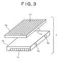
- FIG. 3 is a perspective view showing an assembled condition of an LCD module 1 according to an embodiment of the present invention.
- FIG. 4 is a perspective view of the LCD module 1 of the embodiment.
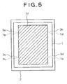
- FIG, 5 is a plan view of the LCD module 1 of the embodiment.
- FIG, 6 is a schematic diagram illustrating a force to be applied to the LCD module 1.
- the LCD module 1 is used, for example, as a display section of a foldable cellular phone or the like constructed by rotatably connecting two cases together.
- the LCD module 1 principally comprises an LCD 1a, a backlight module 1b provided with an LED section 1c, an optical waveguide (not shown), and a light reflector (not shown).
- the LCD 1a, the optical waveguide, and the light reflector or the like are housed in the backlight module 1b.
- the LCD 1a has a non-display section along its peripheral edge portion and the area excluding this non-display section is an LCD display section 1f.
- the side faces of the backlight module 1b are provided with fixing sections 1d, 1e, 1g, and 1h to mount and fix the LCD module 1 to a case (not shown).
- An LED (not shown) of the LED section 1c mounted in the backlight module 1b is a light source of a backlight for the LCD 1a.
- the LCD module 1 is fixed to a case 2 by screws 3(3a through 3d) at the fixing sections 1d, 1e, 1g, and 1h provided on the side faces of the backlight module 1b.
- the LCD module 1 is fixed to the case 2 using the fixing sections 1d, 1e, 1g, and 1h on the side faces of the backlight module 1b so as not to affect the LCD display section 1f.
- the LCD module 1 is fixed, using the side faces of the LCD module 1, to the case 2 from the side faces by screws 3 (3a through 3b), as shown in FIG. 6 .
- screws 3 3a through 3b
- screws which can be removed from the case 2 or wedges which cannot be removed from the case 2 may be used, or these two types may be combined.
- This feature of the present embodiment eliminates the need for the space, in a plan view, for fixing the LCD module 1 at four places on its outside using screws 13a through 13d, which space is required in the conventional liquid crystal display shown in FIG. 2 , thereby making it possible to miniaturize the liquid crystal display, as well as the mobile communication device itself. If the mobile communication device is not designed to be reduced in size, the space required for fixing by the fastening screws 13a through 13d can be used for other parts, and consequently the functionality of the mobile communication device can be improved without changing its size.
- FIG. 7 is a plan view showing a mounted condition of the LCD module 1 shown in FIG. 3 to a case.
- FIG. 7 illustrates a positional relationship between the LED area 1c and the LCD display section 1f, and the case 2. Between the LCD display section 1f and the case 2, there is an area 4 which is irrelevant to display and which begins from both sides of the case 2.
- the area 4 which is irrelevant to display is used chiefly for bonding an optical waveguide and for mounting liquid crystal driving parts for the LCD 1a and is irrelevant to the displaying of the LCD 1a.
- the irrelevant-to-display area 4 is used as areas 5a through 5d for fixing by the fastening screws 3a through 3d, from the side faces.
- the LCD module 1 may have any other circuit boards integrally mounted.
- the LCD module 1 is fixed to the case 2 by the fastening screws 3a and 3b at the fixing areas 1d, 1e, 1g, and 1h on the side faces of the backlight module 1b. Consequently, the space for fixing by the fastening screws 13a through 13d on the outside of the conventional LCD module 12 as shown in Fig. 2 becomes unnecessary, and it is thus possible to package any other functions in that space and to miniaturize the device. Therefore, the present embodiment enables a space for packaging any other functions to be secured, the frame to be narrowed, and the device to be miniaturized without the need for any special attaching parts.
Landscapes
- Physics & Mathematics (AREA)
- Nonlinear Science (AREA)
- Mathematical Physics (AREA)
- Chemical & Material Sciences (AREA)
- Crystallography & Structural Chemistry (AREA)
- General Physics & Mathematics (AREA)
- Optics & Photonics (AREA)
- Liquid Crystal (AREA)
- Devices For Indicating Variable Information By Combining Individual Elements (AREA)
- Telephone Set Structure (AREA)
Claims (4)
- Verfahren zur Montage eines Flüssigkristallanzeigemoduls, umfassend folgende Schritte:Unterbringen einer Flüssigkristallanzeige (1a) in einem Hintergrundbeleuchtungsmodul (1b), das eine lichtemittierende Diode (1c) umfasst, die als Lichtquelle einer Hintergrundbeleuchtung für die Flüssigkristallanzeige (1a) dient, um ein Flüssigkristallanzeigemodul (1) zu bilden; undBefestigen des Flüssigkristallanzeigemoduls (1) mittels eines Befestigungselements (3) an einem Gehäuse (2) durch einen Befestigungsabschnitt, der an einer Seitenfläche des Hintergrundbeleuchtungsmoduls vorgesehen ist.
- Verfahren zur Montage einer Flüssigkristallanzeige nach Anspruch 1, dadurch gekennzeichnet, dass das Gehäuse (2) ein Gehäuse für eine Mobilkommunikationseinrichtung ist.
- Verfahren zur Montage einer Flüssigkristallanzeige nach Anspruch 1, dadurch gekennzeichnet, dass das Gehäuse (2) ein erstes Gehäuse einer Mobilkommunikationseinrichtung ist, die das erste Gehäuse und ein drehbar mit dem ersten Gehäuse verbundenes zweites Gehäuse umfasst.
- Verfahren zur Montage eines Flüssigkristallanzeigemoduls nach einem der Ansprüche 1 bis 3, dadurch gekennzeichnet, dass das Befestigungselement (3) eine Schraube, die aus dem Gehäuse entfernt werden kann, und/oder ein Keil, der nicht aus dem Gehäuse entfernt werden kann, ist.
Applications Claiming Priority (2)
| Application Number | Priority Date | Filing Date | Title |
|---|---|---|---|
| JP2003302228A JP2005070569A (ja) | 2003-08-27 | 2003-08-27 | 移動体通信機及びそれに用いるlcdモジュール実装方法 |
| JP2003302228 | 2003-08-27 |
Publications (3)
| Publication Number | Publication Date |
|---|---|
| EP1510853A1 EP1510853A1 (de) | 2005-03-02 |
| EP1510853B1 true EP1510853B1 (de) | 2013-06-05 |
| EP1510853B9 EP1510853B9 (de) | 2013-10-09 |
Family
ID=34101187
Family Applications (1)
| Application Number | Title | Priority Date | Filing Date |
|---|---|---|---|
| EP04090323.9A Expired - Lifetime EP1510853B9 (de) | 2003-08-27 | 2004-08-21 | Verfahren zur Montage eines Flüssigkristallanzeigemoduls |
Country Status (4)
| Country | Link |
|---|---|
| US (1) | US7403242B2 (de) |
| EP (1) | EP1510853B9 (de) |
| JP (1) | JP2005070569A (de) |
| CN (1) | CN1298191C (de) |
Families Citing this family (10)
| Publication number | Priority date | Publication date | Assignee | Title |
|---|---|---|---|---|
| KR20070059526A (ko) * | 2005-12-07 | 2007-06-12 | 삼성전자주식회사 | 양방향 표시 장치 |
| US7488087B2 (en) * | 2006-05-19 | 2009-02-10 | Honeywell International Inc. | Light guide and display including a light guide |
| CN101377583A (zh) * | 2007-08-31 | 2009-03-04 | 深圳富泰宏精密工业有限公司 | 液晶显示装置 |
| CN101466212B (zh) * | 2007-12-21 | 2012-06-13 | 鸿富锦精密工业(深圳)有限公司 | 电子设备 |
| CN101630070B (zh) * | 2008-07-18 | 2012-10-31 | 龙旗科技(上海)有限公司 | 一种超薄高亮广视角变脸液晶显示模块的设计方法 |
| US8358395B1 (en) | 2010-03-09 | 2013-01-22 | Western Digital Technologies, Inc. | Electronic display assembly comprising a display mount and a flex circuit wrapped around and adhered to the display mount |
| JP5577995B2 (ja) * | 2010-09-28 | 2014-08-27 | 日本精機株式会社 | 表示装置 |
| US9235995B2 (en) * | 2011-12-30 | 2016-01-12 | Eaton Corporation | Panel communication via illuminated bezel |
| CN102879931B (zh) * | 2012-10-18 | 2015-05-20 | 深圳市华星光电技术有限公司 | 窄边框液晶显示装置 |
| CN103024323B (zh) * | 2012-12-07 | 2018-02-06 | 康佳集团股份有限公司 | 一种窄边框液晶电视 |
Family Cites Families (20)
| Publication number | Priority date | Publication date | Assignee | Title |
|---|---|---|---|---|
| JPH0580334A (ja) * | 1991-09-20 | 1993-04-02 | Rohm Co Ltd | 液晶表示装置のバツクライト保持構造 |
| JP3526065B2 (ja) * | 1993-09-29 | 2004-05-10 | シャープ株式会社 | 液晶モジュールの取付け構造 |
| TW373116B (en) * | 1994-12-15 | 1999-11-01 | Sharp Kk | Lighting apparatus |
| JP3027541B2 (ja) * | 1995-09-27 | 2000-04-04 | シャープ株式会社 | 液晶表示装置 |
| JP3296993B2 (ja) * | 1997-04-08 | 2002-07-02 | エルジー フィリップス エルシーディー カンパニー リミテッド | 液晶表示装置を備える携帯用コンピュータ |
| KR100249679B1 (ko) * | 1997-04-10 | 2000-03-15 | 구본준 | 액정표시장치의 백라이트유니트 |
| US6992733B1 (en) * | 1997-04-11 | 2006-01-31 | Micron Technology, Inc. | Backlighting system for an LCD |
| JPH11184392A (ja) | 1997-12-25 | 1999-07-09 | Sanyo Electric Co Ltd | 表示ユニット及び表示装置 |
| JP2000250436A (ja) * | 1999-02-26 | 2000-09-14 | Nec Corp | 薄膜トランジスタアレイ及びその製造方法 |
| JP2001228315A (ja) * | 2000-02-14 | 2001-08-24 | Nitto Denko Corp | 反射板及び液晶表示装置 |
| JP3642263B2 (ja) * | 2000-05-23 | 2005-04-27 | セイコーエプソン株式会社 | 液晶装置及び電子機器 |
| CN1173591C (zh) | 2000-06-16 | 2004-10-27 | 明碁电脑股份有限公司 | 移动电话及将一架体装于该移动电话主印刷电路板的方法 |
| JP4461588B2 (ja) | 2000-08-11 | 2010-05-12 | ソニー株式会社 | 液晶表示装置 |
| JP2002207535A (ja) * | 2001-01-11 | 2002-07-26 | Matsushita Electric Ind Co Ltd | アンテナ内蔵ノート型パソコン |
| CN2484703Y (zh) | 2001-05-09 | 2002-04-03 | 周学良 | 一种折叠式移动电话机 |
| WO2003014816A1 (en) * | 2001-08-02 | 2003-02-20 | Matsushita Electric Industrial Co.,Ltd | Liquid crystal display device |
| KR100793729B1 (ko) * | 2001-09-27 | 2008-01-10 | 삼성전자주식회사 | 액정표시장치 |
| KR100438549B1 (ko) | 2001-11-09 | 2004-07-03 | 엘지전자 주식회사 | 휴대용 단말기의 액정표시장치 |
| JP3687786B2 (ja) * | 2001-11-20 | 2005-08-24 | 日本電気株式会社 | 電子機器及びその表示部クリーニング機構 |
| JP2003223248A (ja) * | 2002-01-29 | 2003-08-08 | Toshiba Corp | 電子機器および無線通信方法 |
-
2003
- 2003-08-27 JP JP2003302228A patent/JP2005070569A/ja active Pending
-
2004
- 2004-08-21 EP EP04090323.9A patent/EP1510853B9/de not_active Expired - Lifetime
- 2004-08-27 CN CNB2004100682577A patent/CN1298191C/zh not_active Expired - Fee Related
- 2004-08-27 US US10/927,001 patent/US7403242B2/en not_active Expired - Fee Related
Also Published As
| Publication number | Publication date |
|---|---|
| CN1591529A (zh) | 2005-03-09 |
| EP1510853B9 (de) | 2013-10-09 |
| EP1510853A1 (de) | 2005-03-02 |
| JP2005070569A (ja) | 2005-03-17 |
| US7403242B2 (en) | 2008-07-22 |
| US20050046766A1 (en) | 2005-03-03 |
| CN1298191C (zh) | 2007-01-31 |
Similar Documents
| Publication | Publication Date | Title |
|---|---|---|
| KR100320664B1 (ko) | 평면표시장치 | |
| JP3789401B2 (ja) | 液晶モジュールおよびそれを用いた液晶モニタ | |
| KR100497925B1 (ko) | 액정 표시 장치 | |
| KR100218581B1 (ko) | 액정표시장치를 가지는 휴대용 컴퓨터 | |
| TWI442130B (zh) | 液晶顯示裝置 | |
| KR100603838B1 (ko) | 액정 표시장치 | |
| KR100787290B1 (ko) | 액정 표시 장치 | |
| US7714953B2 (en) | Display device | |
| KR100596088B1 (ko) | 액정 모듈 | |
| EP1510853B9 (de) | Verfahren zur Montage eines Flüssigkristallanzeigemoduls | |
| JP2008197125A (ja) | 液晶表示装置 | |
| JP4257180B2 (ja) | 両面表示型液晶表示装置 | |
| US10816839B2 (en) | Display device and manufacturing method thereof | |
| JP4746981B2 (ja) | 液晶表示装置、その防塵方法およびその組立方法 | |
| EP1076204B1 (de) | Kantenbeleuchtungs flächenartige Lichquellenvorrichtung, Verfahren zur Herstellung, elektrooptische Einrichtung, und elektronische Geräte | |
| EP0888036B1 (de) | LCD Anordnung mit reduzierter Dicke und Verfahren zum Zusammenbauen | |
| EP1310820B1 (de) | Flüssigkristallanzeige | |
| JP4433898B2 (ja) | 液晶表示装置 | |
| KR100570081B1 (ko) | 액정표시모듈 및 이를 이용한 정보처리장치 | |
| KR100539974B1 (ko) | 엘씨디모듈 | |
| KR100669682B1 (ko) | 휴대폰용 액정표시소자 모듈 조립체 | |
| KR100518726B1 (ko) | 전자카메라 | |
| JP2005294137A (ja) | 光源装置 | |
| JPH10253949A (ja) | 液晶表示装置 | |
| JP2006071694A (ja) | 表示装置 |
Legal Events
| Date | Code | Title | Description |
|---|---|---|---|
| PUAI | Public reference made under article 153(3) epc to a published international application that has entered the european phase |
Free format text: ORIGINAL CODE: 0009012 |
|
| AK | Designated contracting states |
Kind code of ref document: A1 Designated state(s): AT BE BG CH CY CZ DE DK EE ES FI FR GB GR HU IE IT LI LU MC NL PL PT RO SE SI SK TR |
|
| AX | Request for extension of the european patent |
Extension state: AL HR LT LV MK |
|
| 17P | Request for examination filed |
Effective date: 20050110 |
|
| AKX | Designation fees paid |
Designated state(s): DE FR GB IT |
|
| 17Q | First examination report despatched |
Effective date: 20051214 |
|
| GRAP | Despatch of communication of intention to grant a patent |
Free format text: ORIGINAL CODE: EPIDOSNIGR1 |
|
| GRAS | Grant fee paid |
Free format text: ORIGINAL CODE: EPIDOSNIGR3 |
|
| GRAA | (expected) grant |
Free format text: ORIGINAL CODE: 0009210 |
|
| AK | Designated contracting states |
Kind code of ref document: B1 Designated state(s): DE FR GB IT |
|
| REG | Reference to a national code |
Ref country code: GB Ref legal event code: FG4D |
|
| REG | Reference to a national code |
Ref country code: DE Ref legal event code: R081 Ref document number: 602004042335 Country of ref document: DE Owner name: LENOVO INNOVATIONS LIMITED, HK Free format text: FORMER OWNER: NEC CORP., TOKYO, JP |
|
| REG | Reference to a national code |
Ref country code: DE Ref legal event code: R096 Ref document number: 602004042335 Country of ref document: DE Effective date: 20130725 |
|
| PLBE | No opposition filed within time limit |
Free format text: ORIGINAL CODE: 0009261 |
|
| STAA | Information on the status of an ep patent application or granted ep patent |
Free format text: STATUS: NO OPPOSITION FILED WITHIN TIME LIMIT |
|
| 26N | No opposition filed |
Effective date: 20140306 |
|
| PG25 | Lapsed in a contracting state [announced via postgrant information from national office to epo] |
Ref country code: IT Free format text: LAPSE BECAUSE OF FAILURE TO SUBMIT A TRANSLATION OF THE DESCRIPTION OR TO PAY THE FEE WITHIN THE PRESCRIBED TIME-LIMIT Effective date: 20130605 |
|
| REG | Reference to a national code |
Ref country code: DE Ref legal event code: R097 Ref document number: 602004042335 Country of ref document: DE Effective date: 20140306 |
|
| REG | Reference to a national code |
Ref country code: GB Ref legal event code: 732E Free format text: REGISTERED BETWEEN 20141023 AND 20141029 |
|
| REG | Reference to a national code |
Ref country code: FR Ref legal event code: TP Owner name: LENOVO INNOVATIONS LIMITED (HONG KONG), HK Effective date: 20141119 |
|
| REG | Reference to a national code |
Ref country code: FR Ref legal event code: PLFP Year of fee payment: 12 |
|
| PGFP | Annual fee paid to national office [announced via postgrant information from national office to epo] |
Ref country code: FR Payment date: 20150629 Year of fee payment: 12 |
|
| REG | Reference to a national code |
Ref country code: FR Ref legal event code: ST Effective date: 20170428 |
|
| PG25 | Lapsed in a contracting state [announced via postgrant information from national office to epo] |
Ref country code: FR Free format text: LAPSE BECAUSE OF NON-PAYMENT OF DUE FEES Effective date: 20160831 |
|
| REG | Reference to a national code |
Ref country code: DE Ref legal event code: R082 Ref document number: 602004042335 Country of ref document: DE Representative=s name: STORK BAMBERGER PATENTANWAELTE PARTMBB, DE Ref country code: DE Ref legal event code: R081 Ref document number: 602004042335 Country of ref document: DE Owner name: LENOVO INNOVATIONS LIMITED, HK Free format text: FORMER OWNER: NEC CORPORATION, TOKIO/TOKYO, JP Ref country code: DE Ref legal event code: R082 Ref document number: 602004042335 Country of ref document: DE Representative=s name: KASTEL PATENTANWAELTE PARTG MBB, DE |
|
| REG | Reference to a national code |
Ref country code: DE Ref legal event code: R082 Ref document number: 602004042335 Country of ref document: DE Representative=s name: KASTEL PATENTANWAELTE PARTG MBB, DE |
|
| PGFP | Annual fee paid to national office [announced via postgrant information from national office to epo] |
Ref country code: DE Payment date: 20190830 Year of fee payment: 16 |
|
| PGFP | Annual fee paid to national office [announced via postgrant information from national office to epo] |
Ref country code: GB Payment date: 20190829 Year of fee payment: 16 |
|
| REG | Reference to a national code |
Ref country code: DE Ref legal event code: R119 Ref document number: 602004042335 Country of ref document: DE |
|
| GBPC | Gb: european patent ceased through non-payment of renewal fee |
Effective date: 20200821 |
|
| PG25 | Lapsed in a contracting state [announced via postgrant information from national office to epo] |
Ref country code: DE Free format text: LAPSE BECAUSE OF NON-PAYMENT OF DUE FEES Effective date: 20210302 |
|
| PG25 | Lapsed in a contracting state [announced via postgrant information from national office to epo] |
Ref country code: GB Free format text: LAPSE BECAUSE OF NON-PAYMENT OF DUE FEES Effective date: 20200821 |