EP1507152A1 - Optical element having minute periodic structure - Google Patents
Optical element having minute periodic structure Download PDFInfo
- Publication number
- EP1507152A1 EP1507152A1 EP04254863A EP04254863A EP1507152A1 EP 1507152 A1 EP1507152 A1 EP 1507152A1 EP 04254863 A EP04254863 A EP 04254863A EP 04254863 A EP04254863 A EP 04254863A EP 1507152 A1 EP1507152 A1 EP 1507152A1
- Authority
- EP
- European Patent Office
- Prior art keywords
- optical element
- resin layer
- base member
- image
- periodic structure
- Prior art date
- Legal status (The legal status is an assumption and is not a legal conclusion. Google has not performed a legal analysis and makes no representation as to the accuracy of the status listed.)
- Ceased
Links
- 230000003287 optical effect Effects 0.000 title claims abstract description 71
- 230000000737 periodic effect Effects 0.000 title claims abstract description 28
- 239000011347 resin Substances 0.000 claims abstract description 51
- 229920005989 resin Polymers 0.000 claims abstract description 51
- 239000011521 glass Substances 0.000 claims description 24
- 238000000034 method Methods 0.000 claims description 17
- 230000002093 peripheral effect Effects 0.000 claims description 14
- 239000000463 material Substances 0.000 claims description 13
- 238000012545 processing Methods 0.000 claims description 5
- 230000000694 effects Effects 0.000 abstract description 11
- 230000007613 environmental effect Effects 0.000 abstract description 7
- 230000002349 favourable effect Effects 0.000 abstract description 4
- 230000004075 alteration Effects 0.000 description 12
- 230000004907 flux Effects 0.000 description 12
- 230000005540 biological transmission Effects 0.000 description 6
- 238000000465 moulding Methods 0.000 description 6
- 238000004519 manufacturing process Methods 0.000 description 5
- 238000012937 correction Methods 0.000 description 3
- 238000013461 design Methods 0.000 description 3
- 239000004973 liquid crystal related substance Substances 0.000 description 3
- 238000010137 moulding (plastic) Methods 0.000 description 3
- 229920003229 poly(methyl methacrylate) Polymers 0.000 description 3
- 239000004926 polymethyl methacrylate Substances 0.000 description 3
- 230000015572 biosynthetic process Effects 0.000 description 2
- 239000010408 film Substances 0.000 description 2
- ORQBXQOJMQIAOY-UHFFFAOYSA-N nobelium Chemical compound [No] ORQBXQOJMQIAOY-UHFFFAOYSA-N 0.000 description 2
- 239000000758 substrate Substances 0.000 description 2
- 239000010409 thin film Substances 0.000 description 2
- 238000007740 vapor deposition Methods 0.000 description 2
- 102100021943 C-C motif chemokine 2 Human genes 0.000 description 1
- 101000897480 Homo sapiens C-C motif chemokine 2 Proteins 0.000 description 1
- 230000002411 adverse Effects 0.000 description 1
- 239000006121 base glass Substances 0.000 description 1
- 238000001746 injection moulding Methods 0.000 description 1
- 238000003754 machining Methods 0.000 description 1
- 238000012986 modification Methods 0.000 description 1
- 230000004048 modification Effects 0.000 description 1
- 239000004033 plastic Substances 0.000 description 1
- 229920003023 plastic Polymers 0.000 description 1
- 230000009467 reduction Effects 0.000 description 1
- 230000004044 response Effects 0.000 description 1
- 239000004065 semiconductor Substances 0.000 description 1
- 230000001629 suppression Effects 0.000 description 1
- 238000012546 transfer Methods 0.000 description 1
- 238000001771 vacuum deposition Methods 0.000 description 1
- XLYOFNOQVPJJNP-UHFFFAOYSA-N water Substances O XLYOFNOQVPJJNP-UHFFFAOYSA-N 0.000 description 1
Images


Classifications
-
- G—PHYSICS
- G02—OPTICS
- G02B—OPTICAL ELEMENTS, SYSTEMS OR APPARATUS
- G02B5/00—Optical elements other than lenses
- G02B5/18—Diffraction gratings
- G02B5/1814—Diffraction gratings structurally combined with one or more further optical elements, e.g. lenses, mirrors, prisms or other diffraction gratings
Definitions
- the present invention relates to an optical element having a minute periodic structure.
- Spherical lenses or aspheric lenses are used in an image-taking optical system of an image-taking apparatus such as a video camera and a digital still camera and in a projection optical system of a liquid crystal projector or the like.
- Manufacturing methods of the aspheric lenses include a glass grinding method, a glass molding method, a plastic molding method, a replica method (a molding and transfer method).
- Aspheric lenses manufactured through the glass grinding are significantly expensive since each machining takes a long time, although high flexibility is provided in optical design with few limitations on types and sizes of glass materials of the lenses.
- Aspheric lenses formed through the glass molding are relatively inexpensive since they can be manufactured with molds, but only limited types of glass materials can be used.
- Aspheric lenses formed with the plastic molding can be manufactured extremely inexpensively through injection molding, although optical plastic materials are limited in number and have relatively low refractive indexes.
- a resin layer having an aspherical surface is formed on a spherical glass lens serving as a base member.
- types and sizes of glass materials of the base lens are not strictly limited similarly to the aspheric lenses formed through grinding.
- the resin layer having an aspherical surface is relatively inexpensive since it can be manufactured with molding.
- a reflection suppressing coat is typically required on the aspherical surface of the resin in order to reduce ghost and flare caused by reflection on the lens surface in view of the structure in which the aspheric resin layer is formed on the glass lens.
- the replica resin material has a low refractive index and needs high adhesion since it not resistant to significantly increased temperature during the formation of the coat, so that the reflection suppressing coat is typically formed as a multi-layered structure.
- Japanese Patent Application Laid-Open No. 2001-183506 or the like has disclosed an optical element in which a minute periodic (grating) structure having a period (a grating pitch) smaller than the wavelength of incident light is formed on a base member.
- the resin layer has a nonuniform thickness and it varies greatly. If the environmental temperature is changed, complicated and large stress is produced at the surface (the aspherical surface) of the resin since the linear expansion coefficient of the resin is considerably larger than the linear expansion coefficient of the glass and the surface of the resin layer closer to the glass lens is fixed to the glass lens, thereby causing the problem that the reflection suppressing coat comes off or a crack occurs.
- the replica resin layer has a water absorbing property which causes the resin layer to be swelled when the environmental humidity is changed.
- the resin layer has an aspherical surface, and the same problem as described above is presented.
- the replica method When the replica method is used to manufacture an aspherical surface having a small approximate radius of curvature R, the nonuniform thickness of the lens hardly affects the manufacturing and thus the aspherical surface can be formed relatively easily.
- the reflection suppressing coat is formed with a vacuum deposition method on a lens having a small approximate radius of curvature (which is the radius of curvature of a circle defined by the center of an aspherical surface and a point including an effective maximum peripheral portion)
- the thickness of the coat at the center of the lens is different from that in a peripheral portion to prevent realization of desired characteristics.
- the replica lens typically has a multi-layered reflection suppressing film as described above, so that the reflection suppressing property at the center is greatly different from that in the peripheral portion.
- the present invention provides an optical element comprising a base member and a resin layer which is formed on the base member and has a linear expansion coefficient different from that of the base member.
- the resin layer has a minute periodic structure which has a period smaller than a wavelength of incident light on the optical element.
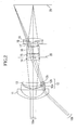
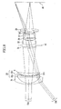
- Fig. 1A shows an image-taking optical system which is Embodiment 1 of the present invention.
- Fig. 1B shows the structure of an image-taking apparatus such as a digital camera and a video camera which uses the image-taking optical system.
- reference numeral 100 shows a body of the image-taking apparatus, and 101 the image-taking optical system.
- Reference numeral 102 shows an image-pickup element formed of a CCD sensor, a CMOS sensor or the like disposed on an image plane of the image-taking optical system 101.
- the image-pickup element 102 photoelectrically converts a subject image formed by the image-taking optical system 101.
- An output signal from the image-pickup element 102 is amplified and A/D converted by an image processing circuit 103 before predetermined processing thereby. In this manner, an image signal is produced.
- the image signal is recorded on a recording medium 104 such as a semiconductor memory, an optical disc, and a magnetic tape.
- reference numerals 1 to 7 show lenses constituting the image-taking optical system.
- Reference numeral 8 shows a stop, and 9 an image plane (the position of an image-pickup device or a film).
- Reference numeral 10a shows a luminous flux (a central luminous flux) which is formed into an image at the center of the image plane 9, while reference numeral 10b shows a luminous flux (a peripheral luminous flux) which is formed into an image in a peripheral portion of the image plane 9.
- the lens 6 has an aspherical surface on the image plane side and is formed with the glass molding method or the plastic molding method.
- the lens 7 has an aspherical surface on the subject side.
- the lens 7 is an aspheric lens formed of a glass lens (a base member) 7a which has spherical surfaces on both sides and a relatively thin resin layer 7b which is formed with the replica method on the spherical surface on the subject side of the glass lens 7a and has an aspherical surface 7c on the subject side.
- the lens 7 is a so-called replica aspheric lens.
- the resin layer 7b is formed, for example, of an ultraviolet curing resin and has a linear expansion coefficient different from that of the glass lens 7a. This also applies to other embodiments.
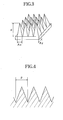
- a minute grating structure (a minute periodic structure) is formed integrally with the aspherical surface.
- the minute grating structure has the sectional profile of triangles (triangular pyramids) as shown in Fig. 4 arranged to be periodic two-dimensionally as shown in Fig. 3 in a period smaller than a wavelength for use (a design wavelength of light incident on the lens, for example a wavelength in a visible light region).
- the minute grating structure formed to be periodic two-dimensionally in this manner can provide a reflection suppressing property with small transmission variations in a vibration direction of light.
- the minute grating structure is formed simultaneously with the formation of the aspherical surface by forming the shape for providing the minute grating structure on a mold for transferring the replica aspherical surface. This can realize the stable aspheric shape and minute grating structure to provide the aspherical surface with the reflection suppressing function by the minute grating structure. In addition, the method can reduce the cost of the replica aspheric lens.
- a grating pitch P which satisfies conditions as a so-called 0th-order grating is selected.
- the minute grating structure is called an SWS (subwave structure) which has a grating pitch smaller than a typical diffraction grating by one or two orders of magnitude and is intended for use of 0th-order light with no diffraction.
- the 0th-order grating is a grating which does not produce diffracted light except 0th-order light in a periodic minute grating structure (see "Optical Society of America Vol.11, No10/October 1994/J.Opt.Soc.Am.A p2695).
- P (ns ⁇ sin ⁇ m-ni ⁇ sin ⁇ i) m ⁇
- P represents a grating pitch
- ni a refractive index of a medium of the grating structure on the incident side
- ⁇ i an incident angle
- ⁇ m a diffraction angle of mth
- ns a refractive index of a medium of the grating structure on the exit side
- m an order of diffraction
- ⁇ a used wavelength a used wavelength
- the value of ⁇ +1 is 90 degrees or more, and the grating pitch P is smaller.
- the incident angle is other than 0 degree, the grating pitch P needs to be further reduced.
- the approximate radius of curvature of the aspheric resin layer is represented by R
- the angle between maximum effective portions (effective maximum peripheral portions) of the aspheric lens which is viewed from the center of radius of curvature R is represented by ⁇
- the following condition is satisfied preferably: 20° ⁇ ⁇ ⁇ 90°
- the approximate radius of curvature refers to the radius of curvature of a circle defined by the center of the aspherical surface and a point including the effective maximum peripheral portion.
- the minute grating structure may be formed such that the structural parameters (such as the shape and dimensions) of the elements of the grating are continuously or step by step changed from the center toward the periphery of the lens.
- the pitch and shape in the grating also vary for providing the optimal reflection suppressing property.
- the grating conditions may be preferably changed in accordance with the desired reflection suppressing property from the center to the periphery.
- the light incident angle varies irregularly with respect to the normal to the surface from the center to the periphery of the lens, so that the optimal grating conditions can be set in accordance with that variation to provide the optimal reflection suppressing effect.
- At least one of the following conditions is satisfied preferably: 0.01 ⁇
- nd1 and nd2 represent the refractive indexes of the resin layer and the base member for a d-line
- vd1 and vd2 represent the Abbe numbers thereof.
- the period (the grating pitch) P of the minute grating structure preferably satisfies the following condition: 100nm ⁇ P ⁇ 350nm
- the condition is provided for achieving the reflection suppressing effect in the wavelength region of visible light (approximately 400 to 700nm) used in the image-taking optical system. If the lower limit is not reached, the difficulty in manufacturing the grating shape is extremely great to increase scattered light due to manufacturing errors. On the other hand, if the upper limit is exceeded, diffracted light is produced in a shorter wavelength region of visible light and becomes flare components to have adverse effects on image performance.
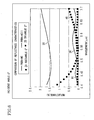
- a broken line 1G shows a reflection characteristic for a central ray (at an incident angle of 0°) on the replica aspherical surface in Embodiment 1 similar to that described in "Optical Society of America" as mentioned above.
- a slid-line 2G shows a reflection characteristic of a single-layered coat (MC) formed on a PMMA (Polymethylmethacrylate) substrate
- a solid-line 3G shows a reflection characteristic of a multi-layered coat (HC11) formed on the PMMA substrate.
- a broken line 11G shows a reflection characteristic for a peripheral ray (at an incident angle of 30°) on the replica aspherical surface.
- a solid-line 12G shows a reflection characteristic of a single-layered coat
- a solid-line 13G shows a reflection characteristic of a multi-layered coat.
- the reflectance is low in the wavelength region of visible light on the replica aspherical surface, and specifically, it is significantly lower than that of the single-layered coat, and lower than that of the multi-layered coat in wavelengths of approximately 0.5 ⁇ m to 0.62 ⁇ m, with an extremely favorable transmission characteristic.
- 0.27979
- 4.81
- P 200 nm
- Fig. 2 shows an image-taking optical system which is Embodiment 2 of the present invention.
- the image-taking optical system is also used in the image-taking apparatus shown in Fig. 1B.
- reference numerals 11 to 19 show lenses constituting the image-taking optical system, 20 a stop, and 21 an image plane.
- Reference numeral 10a shows a luminous flux (a central luminous flux) which is formed into an image at the center of the image plane 21, while reference numeral 10b shows a luminous flux (a peripheral luminous flux) which is formed into an image in a peripheral portion.
- the lens 12 is an aspheric lens having an aspherical surface on the image forming side.
- the lens 12 is a replica aspherical surface formed of a glass lens (a base member) 12a which has spherical surfaces on both sides and a relatively thin resin layer 12b which is formed with the replica method on the spherical surface on the image plane side of the glass lens 12a and has an aspherical surface 12c on the image plane side.
- the resin layer 12b is formed, for example, of an ultraviolet curing resin.
- a minute grating structure is formed integrally with the aspherical surface.
- the minute grating structure has the prism shape (the sectional profile of rectangles) arranged to be periodic two-dimensionally as shown in Fig. 5 in a period smaller than a wavelength of incident light (a wavelength for use).
- the minute grating structure formed to be periodic two-dimensionally in this manner can provide a reflection suppressing property with small transmission variations in a vibration direction of light.
- Embodiment 2 the conditions (4) to (7) are preferably satisfied similarly to Embodiment 1.
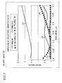
- a broken line 4G shows a reflection characteristic for a central ray (at an incident angle of 0°) on the replica aspherical surface in Embodiment 2.
- a broken line 14G shows a reflection characteristic for a peripheral ray (at an incident angle of 30°) on the replica aspherical surface.
- the reflection characteristic is low in the wavelength region of visible light on the replica aspherical surface, and specifically, it is significantly lower than that of the single-layered coat, and lower than that of the multi-layered coat in wavelengths of approximately 0.47 ⁇ m to 0.60 ⁇ m, with an extremely favorable transmission characteristic.
- Fig. 8 shows an image-taking optical system which is Embodiment 3 of the present invention.
- the image-taking optical system is also used in the image-taking apparatus shown in Fig. 1B.
- reference numerals 31 to 39 show lenses constituting the image-taking optical system, 40 a stop, and 41 an image plane.
- Reference numeral 10a shows a luminous flux (a central luminous flux) which is formed into an image at the center of the image plane 41, while reference numeral 10b shows a luminous flux (a peripheral luminous flux) which is formed into an image in a peripheral portion.
- the lens 32 is an aspheric lens having an aspherical surface on the image plane side.
- the lens 32 is a so-called replica aspherical surface formed of a glass lens (a base member) 32a which has spherical surfaces on both sides and a relatively thin resin layer 32b which is formed with the replica method on the spherical surface on the image plane side of the glass lens 32a and has an aspherical surface 32c on the image plane side.
- the resin layer 32b is formed, for example, of an ultraviolet curing resin.
- a minute grating structure is formed integrally with the aspherical surface.
- the minute grating structure has the triangular pyramid shape (the sectional profile of triangles) as shown in Fig. 4 arranged to be periodic two-dimensionally as shown in Fig. 3 in a period smaller than a wavelength of incident light (a wavelength for use).
- the minute grating structure formed to be periodic two-dimensionally in this manner can provide a reflection suppressing property with small transmission variations in a vibration direction of light.
- Embodiment 3 the conditions (4) to (7) are preferably satisfied similarly to Embodiment 1.
- the resin layer having the minute periodic structure with the pitch smaller than the wavelength of incident light is provided on the lens surface to allow the stable and excellent reflection suppressing effect resistant to changes in environmental characteristics such as temperature and humidity.
- the present invention can be effectively used when the resin layer has a large variation in thickness as in the replica aspherical surface or when the aspherical surface has a smaller radius of curvature, so that the flexibility can be increased in design of an optical system using an aspherical surface.
- the present invention is effective in reducing the size and increasing the performance of the optical system.
- the minute periodic structure can be formed trough molding simultaneously with the replica aspherical surface to effectively achieve a reduction in cost.
- the minute periodic structure can be formed to be periodic two-dimensionally to provide the reflection suppressing effect with small transmission variations in a vibration direction of light.
- the optimal reflection suppressing effect can be provided even when the light incident angle varies irregularly.
- spherical aberration and comatic aberration of the optical system can be effectively corrected in the curvature at the cemented surface between the replica resin layer and the base material, and the surface reflection at the interface between the replica resin layer and the base material can be reduced.
- the correction effects of axial chromatic aberration and chromatic aberration of magnification can be achieved at the cemented surface between the replica resin layer and the base material, and spherical aberration for color produced in the aspheric optical element can be reduced.
- the grating shape is easily manufactured and occurrence of flare components can be reduced.
- Embodiments 1 to 3 While each of Embodiments 1 to 3 has been described for the case where the minute periodic structure is provided for the replica aspheric lens (the optical element) for in the image-taking optical system of a camera, the present invention is applicable to a minute periodic structure provided for a replica aspheric lens used in a projection optical system of an image projection apparatus such as a liquid crystal projector or other optical systems.
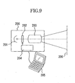
- Fig. 9 shows the structure of an image projection apparatus.
- reference numeral 200 shows a projector body, and 201 a white light source lamp.
- Reference numeral 202 shows an image forming device such as a liquid crystal display panel.
- a drive circuit 204 is connected to the image forming device 202.
- the drive circuit 204 drives the image forming device 202 in response to image information input from an image information supply apparatus 205 such as a personal computer, a DVD player, a VCR, and a television tuner to form an original image on the image forming device 202.
- an image information supply apparatus 205 such as a personal computer, a DVD player, a VCR, and a television tuner to form an original image on the image forming device 202.
- Light from the light source lamp 201 is modulated by the image forming device 202 and projected onto a screen 206 through a projection optical system 203.
- a projection optical system 203 For example, an enlarged version of the original image formed on the image forming device 202 is displayed on the screen 206.
- Embodiments 1 to 3 has been described for the case where the minute periodic structure is provided for the aspheric lens, the present invention is applicable to a minute periodic structure provided for a spherical lens.
Landscapes
- Physics & Mathematics (AREA)
- General Physics & Mathematics (AREA)
- Optics & Photonics (AREA)
- Lenses (AREA)
- Surface Treatment Of Optical Elements (AREA)
- Diffracting Gratings Or Hologram Optical Elements (AREA)
Applications Claiming Priority (2)
| Application Number | Priority Date | Filing Date | Title |
|---|---|---|---|
| JP2003293150A JP2005062526A (ja) | 2003-08-13 | 2003-08-13 | 光学素子および光学系 |
| JP2003293150 | 2003-08-13 |
Publications (1)
| Publication Number | Publication Date |
|---|---|
| EP1507152A1 true EP1507152A1 (en) | 2005-02-16 |
Family
ID=33562796
Family Applications (1)
| Application Number | Title | Priority Date | Filing Date |
|---|---|---|---|
| EP04254863A Ceased EP1507152A1 (en) | 2003-08-13 | 2004-08-12 | Optical element having minute periodic structure |
Country Status (3)
| Country | Link |
|---|---|
| US (1) | US7023630B2 (enExample) |
| EP (1) | EP1507152A1 (enExample) |
| JP (1) | JP2005062526A (enExample) |
Cited By (1)
| Publication number | Priority date | Publication date | Assignee | Title |
|---|---|---|---|---|
| EP1693689A1 (en) * | 2005-02-18 | 2006-08-23 | Canon Kabushiki Kaisha | Optical transparent member and optical system using the same |
Families Citing this family (20)
| Publication number | Priority date | Publication date | Assignee | Title |
|---|---|---|---|---|
| JP2005062525A (ja) * | 2003-08-13 | 2005-03-10 | Canon Inc | 光学素子および光学系 |
| JP2006301474A (ja) * | 2005-04-25 | 2006-11-02 | Sony Corp | ズームレンズ及び撮像装置 |
| JP4803836B2 (ja) * | 2005-08-08 | 2011-10-26 | パナソニック株式会社 | 撮像光学系 |
| WO2007142186A1 (ja) * | 2006-06-06 | 2007-12-13 | Panasonic Corporation | 光学部材 |
| US20100271706A1 (en) * | 2006-06-21 | 2010-10-28 | Panasonic Corporation | Optical member and optical system, optical unit and optical device including the optical member |
| JP4933173B2 (ja) * | 2006-07-03 | 2012-05-16 | 株式会社リコー | 成形品、成形型、光学素子、光学装置、光走査装置、画像表示装置、光ピックアップ装置 |
| US8652040B2 (en) | 2006-12-19 | 2014-02-18 | Valencell, Inc. | Telemetric apparatus for health and environmental monitoring |
| US8157730B2 (en) | 2006-12-19 | 2012-04-17 | Valencell, Inc. | Physiological and environmental monitoring systems and methods |
| US8251903B2 (en) | 2007-10-25 | 2012-08-28 | Valencell, Inc. | Noninvasive physiological analysis using excitation-sensor modules and related devices and methods |
| JP5777682B2 (ja) * | 2008-08-29 | 2015-09-09 | キヤノン株式会社 | 光学素子及びその製造方法、光学系、光学機器 |
| JP5522955B2 (ja) | 2009-02-17 | 2014-06-18 | キヤノン株式会社 | 光学素子の製造方法 |
| US8788002B2 (en) | 2009-02-25 | 2014-07-22 | Valencell, Inc. | Light-guiding devices and monitoring devices incorporating same |
| EP3357419A1 (en) | 2009-02-25 | 2018-08-08 | Valencell, Inc. | Light-guiding devices and monitoring devices incorporating same |
| JP2010266577A (ja) | 2009-05-13 | 2010-11-25 | Canon Inc | 光学系及びそれを有する光学機器 |
| JP2010271533A (ja) * | 2009-05-21 | 2010-12-02 | Canon Inc | 光学素子及びそれを有する光学系 |
| US8888701B2 (en) | 2011-01-27 | 2014-11-18 | Valencell, Inc. | Apparatus and methods for monitoring physiological data during environmental interference |
| US9801552B2 (en) | 2011-08-02 | 2017-10-31 | Valencell, Inc. | Systems and methods for variable filter adjustment by heart rate metric feedback |
| WO2017070463A1 (en) | 2015-10-23 | 2017-04-27 | Valencell, Inc. | Physiological monitoring devices and methods that identify subject activity type |
| US10945618B2 (en) | 2015-10-23 | 2021-03-16 | Valencell, Inc. | Physiological monitoring devices and methods for noise reduction in physiological signals based on subject activity type |
| WO2018009736A1 (en) | 2016-07-08 | 2018-01-11 | Valencell, Inc. | Motion-dependent averaging for physiological metric estimating systems and methods |
Citations (5)
| Publication number | Priority date | Publication date | Assignee | Title |
|---|---|---|---|---|
| US5694247A (en) * | 1994-05-02 | 1997-12-02 | U.S. Philips Corporation | Optical transmissive component with anti-reflection gratings |
| US5726805A (en) * | 1996-06-25 | 1998-03-10 | Sandia Corporation | Optical filter including a sub-wavelength periodic structure and method of making |
| US20020118465A1 (en) * | 2001-02-28 | 2002-08-29 | Konica Corporation | Molding die for optical element, optical element and master die |
| EP1241490A2 (en) * | 2001-03-12 | 2002-09-18 | CSEM Centre Suisse d'Electronique et de Microtechnique SA | Polarisers and mass-production method |
| EP1260847A2 (en) * | 2001-05-25 | 2002-11-27 | Canon Kabushiki Kaisha | Optical element, scanning optical system having the same, and image forming apparatus |
Family Cites Families (3)
| Publication number | Priority date | Publication date | Assignee | Title |
|---|---|---|---|---|
| GB9509487D0 (en) * | 1995-05-10 | 1995-07-05 | Ici Plc | Micro relief element & preparation thereof |
| JPH10161020A (ja) * | 1996-12-02 | 1998-06-19 | Olympus Optical Co Ltd | 回折光学素子を用いた撮影光学系 |
| JP2001183506A (ja) | 1999-12-24 | 2001-07-06 | Sony Corp | 光学素子及び表示装置 |
-
2003
- 2003-08-13 JP JP2003293150A patent/JP2005062526A/ja active Pending
-
2004
- 2004-08-09 US US10/913,332 patent/US7023630B2/en not_active Expired - Lifetime
- 2004-08-12 EP EP04254863A patent/EP1507152A1/en not_active Ceased
Patent Citations (5)
| Publication number | Priority date | Publication date | Assignee | Title |
|---|---|---|---|---|
| US5694247A (en) * | 1994-05-02 | 1997-12-02 | U.S. Philips Corporation | Optical transmissive component with anti-reflection gratings |
| US5726805A (en) * | 1996-06-25 | 1998-03-10 | Sandia Corporation | Optical filter including a sub-wavelength periodic structure and method of making |
| US20020118465A1 (en) * | 2001-02-28 | 2002-08-29 | Konica Corporation | Molding die for optical element, optical element and master die |
| EP1241490A2 (en) * | 2001-03-12 | 2002-09-18 | CSEM Centre Suisse d'Electronique et de Microtechnique SA | Polarisers and mass-production method |
| EP1260847A2 (en) * | 2001-05-25 | 2002-11-27 | Canon Kabushiki Kaisha | Optical element, scanning optical system having the same, and image forming apparatus |
Non-Patent Citations (2)
| Title |
|---|
| GALE M T: "Replication techniques for diffractive optical elements", MICROELECTRONIC ENGINEERING, ELSEVIER PUBLISHERS BV., AMSTERDAM, NL, vol. 34, no. 3-4, 1 December 1997 (1997-12-01), pages 321 - 339, XP004108296, ISSN: 0167-9317 * |
| GOMBERT A ET AL: "Antireflective submicrometer surface-relief gratings for solar applications", SOLAR ENERGY MATERIALS AND SOLAR CELLS, ELSEVIER SCIENCE PUBLISHERS, AMSTERDAM, NL, vol. 54, no. 1-4, July 1998 (1998-07-01), pages 333 - 342, XP004148903, ISSN: 0927-0248 * |
Cited By (1)
| Publication number | Priority date | Publication date | Assignee | Title |
|---|---|---|---|---|
| EP1693689A1 (en) * | 2005-02-18 | 2006-08-23 | Canon Kabushiki Kaisha | Optical transparent member and optical system using the same |
Also Published As
| Publication number | Publication date |
|---|---|
| US7023630B2 (en) | 2006-04-04 |
| US20050036212A1 (en) | 2005-02-17 |
| JP2005062526A (ja) | 2005-03-10 |
Similar Documents
| Publication | Publication Date | Title |
|---|---|---|
| EP1507152A1 (en) | Optical element having minute periodic structure | |
| JP4817076B2 (ja) | 回折光学素子 | |
| CN101952761B (zh) | 摄像透镜、摄像装置、便携终端及摄像透镜的制造方法 | |
| KR20130016223A (ko) | 광학 유닛 및 촬상 장치 | |
| US20220107482A1 (en) | Electronic device | |
| TWI413795B (zh) | 攝影透鏡以及照相機 | |
| KR20090113290A (ko) | 촬상 렌즈, 촬상 장치, 휴대 단말기, 및 촬상 렌즈의 제조 방법 | |
| EP1602958A1 (en) | Imaging lens | |
| CN102576143A (zh) | 光学单元和摄像装置 | |
| WO2022239661A1 (ja) | 撮像レンズ系及び撮像装置 | |
| US20100321782A1 (en) | Optical element and optical system including the same | |
| US11640046B2 (en) | Lens system and electronic device | |
| WO2012011416A1 (ja) | 光学ユニットおよび撮像装置 | |
| JP2004205813A (ja) | ズームレンズ | |
| JP2006126494A (ja) | 撮像レンズ | |
| JP2004252101A (ja) | 超広角レンズ | |
| KR100332018B1 (ko) | 이미지 센싱 모듈 | |
| JP5434450B2 (ja) | 光学ユニットおよび撮像装置 | |
| JP2004219782A (ja) | 撮像光学系 | |
| JP5589509B2 (ja) | 光学ユニットおよび撮像装置 | |
| JP2004212639A (ja) | 回折光学素子を備えたカタディオプトリックレンズ | |
| US7256947B2 (en) | Optical element having minute periodic structure | |
| US20230168413A1 (en) | Optical system and image capturing apparatus including the same | |
| US20250028154A1 (en) | Optical system and imaging apparatus including the same | |
| JP2025110319A (ja) | 光学系及び撮像装置 |
Legal Events
| Date | Code | Title | Description |
|---|---|---|---|
| PUAI | Public reference made under article 153(3) epc to a published international application that has entered the european phase |
Free format text: ORIGINAL CODE: 0009012 |
|
| AK | Designated contracting states |
Kind code of ref document: A1 Designated state(s): AT BE BG CH CY CZ DE DK EE ES FI FR GB GR HU IE IT LI LU MC NL PL PT RO SE SI SK TR |
|
| AX | Request for extension of the european patent |
Extension state: AL HR LT LV MK |
|
| 17P | Request for examination filed |
Effective date: 20050701 |
|
| AKX | Designation fees paid |
Designated state(s): AT BE BG CH CY CZ DE DK EE ES FI FR GB GR HU IE IT LI LU MC NL PL PT RO SE SI SK TR |
|
| 17Q | First examination report despatched |
Effective date: 20050804 |
|
| STAA | Information on the status of an ep patent application or granted ep patent |
Free format text: STATUS: THE APPLICATION HAS BEEN REFUSED |
|
| 18R | Application refused |
Effective date: 20080429 |