EP1503473A1 - Circuit integré monolithique pour la protection contre les surtensions - Google Patents
Circuit integré monolithique pour la protection contre les surtensions Download PDFInfo
- Publication number
- EP1503473A1 EP1503473A1 EP04017574A EP04017574A EP1503473A1 EP 1503473 A1 EP1503473 A1 EP 1503473A1 EP 04017574 A EP04017574 A EP 04017574A EP 04017574 A EP04017574 A EP 04017574A EP 1503473 A1 EP1503473 A1 EP 1503473A1
- Authority
- EP
- European Patent Office
- Prior art keywords
- diode
- voltage
- terminal
- zener diode
- connection
- Prior art date
- Legal status (The legal status is an assumption and is not a legal conclusion. Google has not performed a legal analysis and makes no representation as to the accuracy of the status listed.)
- Granted
Links
- 230000015556 catabolic process Effects 0.000 claims description 4
- 230000008054 signal transmission Effects 0.000 claims description 3
- 230000002401 inhibitory effect Effects 0.000 abstract 1
- 239000000758 substrate Substances 0.000 description 17
- 230000007246 mechanism Effects 0.000 description 14
- 238000010586 diagram Methods 0.000 description 9
- 230000005540 biological transmission Effects 0.000 description 5
- 230000006378 damage Effects 0.000 description 5
- 238000010521 absorption reaction Methods 0.000 description 2
- 230000001681 protective effect Effects 0.000 description 2
- 230000008878 coupling Effects 0.000 description 1
- 238000010168 coupling process Methods 0.000 description 1
- 238000005859 coupling reaction Methods 0.000 description 1
- 238000005516 engineering process Methods 0.000 description 1
- 238000011156 evaluation Methods 0.000 description 1
- 230000001939 inductive effect Effects 0.000 description 1
- 238000003780 insertion Methods 0.000 description 1
- 230000037431 insertion Effects 0.000 description 1
- 230000007257 malfunction Effects 0.000 description 1
- 238000004519 manufacturing process Methods 0.000 description 1
- 230000003071 parasitic effect Effects 0.000 description 1
- 238000011084 recovery Methods 0.000 description 1
Images

Classifications
-
- H—ELECTRICITY
- H01—ELECTRIC ELEMENTS
- H01L—SEMICONDUCTOR DEVICES NOT COVERED BY CLASS H10
- H01L27/00—Devices consisting of a plurality of semiconductor or other solid-state components formed in or on a common substrate
- H01L27/02—Devices consisting of a plurality of semiconductor or other solid-state components formed in or on a common substrate including semiconductor components specially adapted for rectifying, oscillating, amplifying or switching and having potential barriers; including integrated passive circuit elements having potential barriers
- H01L27/0203—Particular design considerations for integrated circuits
- H01L27/0248—Particular design considerations for integrated circuits for electrical or thermal protection, e.g. electrostatic discharge [ESD] protection
- H01L27/0251—Particular design considerations for integrated circuits for electrical or thermal protection, e.g. electrostatic discharge [ESD] protection for MOS devices
- H01L27/0255—Particular design considerations for integrated circuits for electrical or thermal protection, e.g. electrostatic discharge [ESD] protection for MOS devices using diodes as protective elements
-
- H—ELECTRICITY
- H01—ELECTRIC ELEMENTS
- H01L—SEMICONDUCTOR DEVICES NOT COVERED BY CLASS H10
- H01L2924/00—Indexing scheme for arrangements or methods for connecting or disconnecting semiconductor or solid-state bodies as covered by H01L24/00
- H01L2924/0001—Technical content checked by a classifier
- H01L2924/0002—Not covered by any one of groups H01L24/00, H01L24/00 and H01L2224/00
Definitions
- the invention relates to a monolithically integrable circuit arrangement for overvoltage protection of one or more connections an integrated circuit according to the preamble of the claim 1.
- ESD electrostatic discharge
- circuit arrangements for overvoltage protection monolithically integrated into the integrated circuit to be protected because discrete or external components significantly increase the circuit design complicate and ensure no corresponding operational safety can.
- the invention is a technical problem of providing a monolithic integrable circuit arrangement for overvoltage protection based on the type mentioned, the positive and / or negative Overvoltages on terminals of an integrated circuit effectively limited, distortions of a useful signal by clamp mechanisms largely prevented and inexpensive without special components can be produced.
- the invention solves this problem by providing a circuit arrangement with the features of claim 1 or 2.
- circuit arrangement according to claim 1 or 2 are as surge protection of one or more connections a low-side driver stage or a high-side driver stage for the Connection or at least one of the terminals in each case a first Zener diode and a first diode provided in series between the Connection and the reference potential are looped, wherein the first Zener diode in the flow direction and the first diode connected in the reverse direction are.
- the first diode prevents the first zener diode from being switched on positive voltages at the connection.
- For negative voltages at Connection operates the first diode in the forward direction and the Zener diode in the reverse direction. If the negative voltage at the connection is the Zener voltage of the first Zener diode and the forward voltage of the exceeds the first diode, one of the first zener diode and the first diode formed current path and the voltage at the input is based on the sum of zener voltage and diode current voltage limited. In particular, the first Zener diode takes the energy negative ESD pulses on, causing a destruction of the circuit is prevented. By a suitable choice of the zener voltage, the Threshold set until the clamp mechanism is inserted become.
- an n-channel MOSFET is assigned, for the connection or at least one of the Connections further a second diode between this terminal and a connection of the n-channel MOSFET in the flow direction looped and a second Zener diode is between the terminal of the n-channel MOSFET and the reference potential looped in the reverse direction.
- the second diode prevents a negative terminal voltages Current flow through a bulk diode of the n-channel MOSFET, this between its drain terminal and reference potential.
- the second Zener diode is used to limit a positive terminal voltage to a maximum value and is used in particular for energy absorption positive ESD pulses, which prevents destruction of the circuit becomes.
- the positive voltage at the terminal is the Zener voltage
- the second Zener diode and the forward voltage of the second diode exceeds, one of the second Zener diode and the second diode formed current path and the voltage at the input is on the sum of Zener voltage and diode flow voltage limited.
- the voltage threshold be adjusted until insertion of the clamp mechanism.
- a p-channel MOSFET is assigned, for the connection or at least one of the Connections further a second diode between the supply voltage and a connection of the p-channel MOSFET in the flow direction looped in and a second zener diode is between the connector of the p-channel MOSFET and the reference potential in the reverse direction looped.
- the second diode prevents positive terminal voltages, the are greater than the supply voltage, a current flow through a Bulk diode of the p-channel MOSFET, which this between its drain terminal and its source terminal, into the supply voltage.
- the second Zener diode is used to limit a positive Terminal voltage to a maximum value and is used in particular for Energy absorption of positive ESD pulses, causing destruction of the Circuit is prevented.
- the positive voltage at the terminal the zener voltage of the second Zener diode and the forward voltage exceeds the bulk diode, one of the second zener diode and the bulk diode formed current path conductive and the voltage at Input is to the sum of Zener voltage and diode flow voltage limited.
- suitable choice of the zener voltage can the voltage threshold until the onset of the clamp mechanism be set.
- the respective Zener diode has a breakdown voltage in a range of 30V up 50V and / or the respective diode a breakdown voltage in one Range from 50V to 60V. Such dimensioning allows safe operation over a wide voltage range, good on the typically occurring interference voltages is adjusted.
- this serves for Overvoltage protection of a connection of a low-side driver stage and a port of a high-side driver stage, which together Form terminal pair for differential signal transmission.
- the circuit arrangement allows effective protection against both positive as well as against negative overvoltages, with the usual Noise or overvoltage amounts do not use a clamp mechanism and consequently no signal corruption occurs. This allows a secure differential signal transmission even in disturbed environments such as for example, in the motor vehicle.
- this serves for Overvoltage protection of a transmitter / receiver circuit for a bus system, especially for a CAN bus.
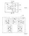
- Fig. 1 shows a block diagram of an integrated circuit IS for differential Data transmission with a high-side driver stage HS and a low-side driver stage LS, whose connections AHS and ALS respectively by a circuit arrangement according to the invention against overvoltage are protected.
- the driver stages LS and HS are each with a transmitter / receiver unit SE, which is used to control the driver stages HS and LS as well as for the evaluation of signals at the connections AHS and ALS serve.
- the integrated circuit IS is connected via a Supply voltage connection VA with a supply voltage from e.g. 5V supplied.
- a reference voltage of e.g. OV is located on one Reference voltage connection BA on.
- Fig. 2 shows a circuit diagram of the low-side driver stage LS of Fig. 1.
- Die Driver stage LS comprises a switching means in the form of an n-channel MOSFET NM, the connection ALS depending on a through the transmitter / receiver unit SE generated drive signal with the Reference potential connects.
- the n-channel MOSFET NM has a substrate Bulk diode SD1 between its drain and reference potential on.
- a Zener diode ZD1 and a diode D1 are connected in series between the terminals ALS and the reference potential looped in, wherein the zener diode ZD1 in the flow direction and the diode D1 connected in the reverse direction are.
- the Zener diode ZD1 and the diode D1 have a substrate diode SD2 or SD3 in the reverse direction between their respective cathode and reference potential.
- the diode D1 prevents a connection of the Zener diode ZD1 in positive Voltages at connection ALS.
- For negative voltages at Terminal ALS operates the diode D1 in the forward direction and the zener diode ZD1 in reverse direction.
- the diode D1 exceeds that of Zener diode ZD1 and diode D1 formed current path and the voltage at the terminal ALS is based on the sum of zener voltage and diode current voltage limited.
- suitable choice of the zener voltage can the voltage threshold until the onset of the clamp mechanism be set.
- a diode D2 which is between the terminal ALS and the drain terminal of the transistor NM is looped in the flow direction prevented at negative terminal voltages a current flow through the Substrate diode SD1 of the n-channel MOSFET.
- the diode D2 has a Substrate diode SD4 between its cathode and reference potential.
- a Zener diode ZD2 which is between the drain terminal of the transistor NM and the reference potential is looped in the reverse direction, is used for Limitation of a positive terminal voltage to a maximum value.
- the Zener diode ZD2 has a substrate diode SD5 between its cathode and reference potential.
- Fig. 3 shows a circuit diagram of the high-side driver stage HS of Fig. 1.
- Die Driver stage HS comprises a switching means in the form of a p-channel MOSFET PM, the connection AHS depending on a through the transmitter / receiver unit SE generated drive signal with the Supply voltage connects.
- the p-channel MOSFET PM has a Substrate or bulk diode SD6 between its drain terminal and its source connection.
- a diode D3 is between the supply voltage and the drain terminal of the transistor PM is looped in the flow direction and has a substrate diode SD7 in the reverse direction between its cathode and the reference potential. It prevents positive connection voltages, which are greater than the supply voltage, a current flow through the substrate diode SD6 of the p-channel MOSFET PM in the supply voltage.
- a zener diode ZD3 which is between the drain terminal of the transistor PM and the reference potential is looped in the reverse direction, is used for Limitation of a positive terminal voltage to a maximum value.
- Zener diode ZD3 has a substrate diode SD8 between its cathode and reference potential.
- the zener diode ZD3 and substrate diode SD6 formed current path conductive and the voltage at the input is based on the sum of zener voltage and Diode supply voltage limited.
- a Zener diode ZD1 ', its associated substrate diode SD2', a diode D1 'and its associated substrate diode SD3' correspond in their Interconnection, function and dimensioning shown in Fig. 2 Components ZD1, SD2, D1 or SD3.
- FIG. 4 shows a diagram of the current-voltage characteristic between the terminals AHS and ALS of Fig. 1.
- the zener diodes are dimensioned such that a clamp mechanism only used at signal amplitudes of greater than ⁇ 45V.
- the input signals become practical not distorted, resulting in safe signal recovery from the Differential signal of the connections AHS and ALS is guaranteed.
- the present invention enables as described above Embodiments will become clear, an effective limitation of positive and negative surges at terminals of an integrated Circuit. Falsifications of a useful signal by clamp mechanisms occur only at very high overvoltages.
- the Circuit arrangement is inexpensive to produce and in a simple manner monolithic integrated, since they are no expensive special components, For example, substrate-free poly elements and no consuming Manufacturing technologies required. It is for example for CAN transceiver, but also for any other integrated transmitter / receiver circuits usable where an overvoltage protection is desired, without external components for surge protection to be realized.
Landscapes
- Engineering & Computer Science (AREA)
- Power Engineering (AREA)
- Physics & Mathematics (AREA)
- Condensed Matter Physics & Semiconductors (AREA)
- General Physics & Mathematics (AREA)
- Computer Hardware Design (AREA)
- Microelectronics & Electronic Packaging (AREA)
- Emergency Protection Circuit Devices (AREA)
- Semiconductor Integrated Circuits (AREA)
- Logic Circuits (AREA)
- Metal-Oxide And Bipolar Metal-Oxide Semiconductor Integrated Circuits (AREA)
- Electronic Switches (AREA)
Applications Claiming Priority (2)
| Application Number | Priority Date | Filing Date | Title |
|---|---|---|---|
| DE10335383 | 2003-07-28 | ||
| DE10335383A DE10335383A1 (de) | 2003-07-28 | 2003-07-28 | Monolithisch integrierbare Schaltungsanordnung zum Überspannungsschutz |
Publications (2)
| Publication Number | Publication Date |
|---|---|
| EP1503473A1 true EP1503473A1 (fr) | 2005-02-02 |
| EP1503473B1 EP1503473B1 (fr) | 2009-07-01 |
Family
ID=33521533
Family Applications (1)
| Application Number | Title | Priority Date | Filing Date |
|---|---|---|---|
| EP04017574A Expired - Lifetime EP1503473B1 (fr) | 2003-07-28 | 2004-07-24 | Circuit integré monolithique pour la protection contre les surtensions |
Country Status (3)
| Country | Link |
|---|---|
| US (1) | US7130175B2 (fr) |
| EP (1) | EP1503473B1 (fr) |
| DE (2) | DE10335383A1 (fr) |
Families Citing this family (5)
| Publication number | Priority date | Publication date | Assignee | Title |
|---|---|---|---|---|
| DE10251473B3 (de) * | 2002-11-05 | 2004-06-17 | Siemens Ag | Schutzschaltung zum Schutz gegen Überspannung für einen CAN-Bus-Transceiver |
| DE102006021747A1 (de) * | 2006-05-10 | 2007-11-15 | Robert Bosch Gmbh | Schutzschaltung |
| US8116057B2 (en) | 2006-12-21 | 2012-02-14 | Apple Inc. | Data port transient protection apparatus and methods |
| US8699189B2 (en) | 2012-05-22 | 2014-04-15 | Honeywell International Inc. | High precision clipping regulator circuit |
| DE102021203501A1 (de) | 2021-04-09 | 2022-10-13 | Robert Bosch Gesellschaft mit beschränkter Haftung | Schutzschaltung für CAN-Transceiver |
Citations (3)
| Publication number | Priority date | Publication date | Assignee | Title |
|---|---|---|---|---|
| US5448180A (en) | 1991-03-16 | 1995-09-05 | Robert Bosch Gmbh | Transmitter end stage |
| US5986862A (en) * | 1996-12-31 | 1999-11-16 | Lg Semicon Co., Ltd. | Electrostatic discharge protection circuit |
| EP1178531A1 (fr) * | 2000-08-05 | 2002-02-06 | Philips Corporate Intellectual Property GmbH | Circuit de protection d'entrée pour dispositif semi-conducteur CMOS |
Family Cites Families (6)
| Publication number | Priority date | Publication date | Assignee | Title |
|---|---|---|---|---|
| NL7614118A (nl) * | 1976-12-20 | 1978-06-22 | Philips Nv | Schakeling voor het beschermen van telefoon- lijnen. |
| DE4407279C1 (de) | 1994-03-04 | 1994-10-13 | Siemens Ag | Halbleiterbauelement für den Überspannungsschutz von MOSFET und IGBT |
| DE69527146T2 (de) | 1995-11-10 | 2002-12-12 | Co.Ri.M.Me. Consorzio Per La Ricerca Sulla Microelettronica Nel Mezzogiorno, Catania | Integriertes MOS-Bauelement mit einer Gateschutzdiode |
| JPH10189761A (ja) * | 1996-12-20 | 1998-07-21 | Fuji Electric Co Ltd | 半導体装置 |
| ATE456861T1 (de) * | 1999-06-01 | 2010-02-15 | Imec | Esd-schutz-bauteil für mittlere triggerspannung |
| DE10233220B3 (de) * | 2002-07-22 | 2004-05-19 | Texas Instruments Deutschland Gmbh | Komparator mit Hysterese |
-
2003
- 2003-07-28 DE DE10335383A patent/DE10335383A1/de not_active Withdrawn
-
2004
- 2004-07-24 EP EP04017574A patent/EP1503473B1/fr not_active Expired - Lifetime
- 2004-07-24 DE DE502004009683T patent/DE502004009683D1/de not_active Expired - Lifetime
- 2004-07-27 US US10/900,643 patent/US7130175B2/en active Active
Patent Citations (3)
| Publication number | Priority date | Publication date | Assignee | Title |
|---|---|---|---|---|
| US5448180A (en) | 1991-03-16 | 1995-09-05 | Robert Bosch Gmbh | Transmitter end stage |
| US5986862A (en) * | 1996-12-31 | 1999-11-16 | Lg Semicon Co., Ltd. | Electrostatic discharge protection circuit |
| EP1178531A1 (fr) * | 2000-08-05 | 2002-02-06 | Philips Corporate Intellectual Property GmbH | Circuit de protection d'entrée pour dispositif semi-conducteur CMOS |
Also Published As
| Publication number | Publication date |
|---|---|
| DE502004009683D1 (de) | 2009-08-13 |
| US7130175B2 (en) | 2006-10-31 |
| EP1503473B1 (fr) | 2009-07-01 |
| DE10335383A1 (de) | 2005-02-24 |
| US20050024801A1 (en) | 2005-02-03 |
Similar Documents
| Publication | Publication Date | Title |
|---|---|---|
| EP0576444B1 (fr) | Etage final d'emetteur integre monolithique | |
| DE102009061073B4 (de) | Halbleitervorrichtung mit Impedanzsteuerschaltung | |
| DE102005043907B4 (de) | Halbleiterschaltungen und Übertragungsvorrichtungen zur fehlersicheren Kommunikation in Kraftfahrzeugen | |
| WO1990009713A1 (fr) | Interface de reseau | |
| DE19728783A1 (de) | Überspannungsschutzschaltung, insbesondere für Eingänge integrierter Schaltungen | |
| DE102007053089B4 (de) | Elektrisches und elektronisches System | |
| EP1503473B1 (fr) | Circuit integré monolithique pour la protection contre les surtensions | |
| WO2007073930A2 (fr) | Circuiterie de commutation pourvue d'un dispositif de protection contre les explosions | |
| EP0495142B1 (fr) | Protection contre l'inversion de polarité et contre les surtensions pour des circuits | |
| DE2644401C2 (de) | Elektronischer Schalter | |
| DE4428115C2 (de) | Steuergerät mit einer Schaltungsanordnung zum Schutz des Steuergerätes bei Unterbrechung der Steuergerätemasse | |
| EP3788654B1 (fr) | Circuit de protection contre les décharges électrostatiques | |
| DE102007018237A1 (de) | Schaltung mit verbessertem ESD-Schutz bei repetierender Pulsbelastung | |
| DE102006021747A1 (de) | Schutzschaltung | |
| DE102011053904A1 (de) | Schaltungsanordnung zum Schutz von Transceivern von Schnittstellen für drahtgebundene Kommunikation | |
| DE10349092A1 (de) | Integrierte Schaltungsanordnung zum Erkennen und Ausgeben von Steuersignalen | |
| DE10008180A1 (de) | Elektronische Gebereinrichtung | |
| DE10200518B4 (de) | Spannungsbegrenzer für den Schnittstellenkreis eines Kommunikationsbusses | |
| DE69601198T2 (de) | Kurzschlussschutz für einen Audio-Video-Datenbus | |
| EP1069407A1 (fr) | Capteur électronique | |
| DE10007607B4 (de) | Ausfallsichere Überspannungsschutzschaltung | |
| DE19633723C1 (de) | Verzögerungsarmer Pegelumsetzer mit Schutzschaltung | |
| EP0766399B1 (fr) | Circuit d'attaque bidirectionnel pour système de bus PCI | |
| DE4222279C1 (de) | Anordnung zur Übertragung von Signalen | |
| DE69620529T2 (de) | Ausgangsstufe mit Schutz gegen externe Überspannungen am Ausgang im abgeschalteten, hochimpedanten Zustand |
Legal Events
| Date | Code | Title | Description |
|---|---|---|---|
| PUAI | Public reference made under article 153(3) epc to a published international application that has entered the european phase |
Free format text: ORIGINAL CODE: 0009012 |
|
| AK | Designated contracting states |
Kind code of ref document: A1 Designated state(s): AT BE BG CH CY CZ DE DK EE ES FI FR GB GR HU IE IT LI LU MC NL PL PT RO SE SI SK TR |
|
| AX | Request for extension of the european patent |
Extension state: AL HR LT LV MK |
|
| 17P | Request for examination filed |
Effective date: 20050111 |
|
| AKX | Designation fees paid |
Designated state(s): DE FR GB |
|
| 17Q | First examination report despatched |
Effective date: 20070326 |
|
| GRAP | Despatch of communication of intention to grant a patent |
Free format text: ORIGINAL CODE: EPIDOSNIGR1 |
|
| RTI1 | Title (correction) |
Free format text: MONOLITHICALLY INTEGRATED CIRCUIT FOR OVERVOLTAGE PROTECTION |
|
| GRAS | Grant fee paid |
Free format text: ORIGINAL CODE: EPIDOSNIGR3 |
|
| GRAA | (expected) grant |
Free format text: ORIGINAL CODE: 0009210 |
|
| AK | Designated contracting states |
Kind code of ref document: B1 Designated state(s): DE FR GB |
|
| REG | Reference to a national code |
Ref country code: GB Ref legal event code: FG4D Free format text: NOT ENGLISH |
|
| REF | Corresponds to: |
Ref document number: 502004009683 Country of ref document: DE Date of ref document: 20090813 Kind code of ref document: P |
|
| RAP2 | Party data changed (patent owner data changed or rights of a patent transferred) |
Owner name: ATMEL AUTOMOTIVE GMBH |
|
| PLBE | No opposition filed within time limit |
Free format text: ORIGINAL CODE: 0009261 |
|
| STAA | Information on the status of an ep patent application or granted ep patent |
Free format text: STATUS: NO OPPOSITION FILED WITHIN TIME LIMIT |
|
| 26N | No opposition filed |
Effective date: 20100406 |
|
| PG25 | Lapsed in a contracting state [announced via postgrant information from national office to epo] |
Ref country code: FR Free format text: LAPSE BECAUSE OF NON-PAYMENT OF DUE FEES Effective date: 20090901 |
|
| REG | Reference to a national code |
Ref country code: FR Ref legal event code: ST Effective date: 20100930 |
|
| PG25 | Lapsed in a contracting state [announced via postgrant information from national office to epo] |
Ref country code: GB Free format text: LAPSE BECAUSE OF NON-PAYMENT OF DUE FEES Effective date: 20091001 |
|
| REG | Reference to a national code |
Ref country code: DE Ref legal event code: R082 Ref document number: 502004009683 Country of ref document: DE Representative=s name: GRUENECKER, KINKELDEY, STOCKMAIR & SCHWANHAEUS, DE Effective date: 20130529 Ref country code: DE Ref legal event code: R081 Ref document number: 502004009683 Country of ref document: DE Owner name: ATMEL CORP., US Free format text: FORMER OWNER: ATMEL AUTOMOTIVE GMBH, 74072 HEILBRONN, DE Effective date: 20130529 Ref country code: DE Ref legal event code: R081 Ref document number: 502004009683 Country of ref document: DE Owner name: ATMEL CORP., SAN JOSE, US Free format text: FORMER OWNER: ATMEL AUTOMOTIVE GMBH, 74072 HEILBRONN, DE Effective date: 20130529 Ref country code: DE Ref legal event code: R082 Ref document number: 502004009683 Country of ref document: DE Representative=s name: GRUENECKER PATENT- UND RECHTSANWAELTE PARTG MB, DE Effective date: 20130529 |
|
| P01 | Opt-out of the competence of the unified patent court (upc) registered |
Effective date: 20230528 |
|
| PGFP | Annual fee paid to national office [announced via postgrant information from national office to epo] |
Ref country code: DE Payment date: 20230620 Year of fee payment: 20 |
|
| REG | Reference to a national code |
Ref country code: DE Ref legal event code: R071 Ref document number: 502004009683 Country of ref document: DE |