EP1503438A2 - Substrate for optical element, organic electroluminescence element and organic electoluminescence display device - Google Patents
Substrate for optical element, organic electroluminescence element and organic electoluminescence display device Download PDFInfo
- Publication number
- EP1503438A2 EP1503438A2 EP04090293A EP04090293A EP1503438A2 EP 1503438 A2 EP1503438 A2 EP 1503438A2 EP 04090293 A EP04090293 A EP 04090293A EP 04090293 A EP04090293 A EP 04090293A EP 1503438 A2 EP1503438 A2 EP 1503438A2
- Authority
- EP
- European Patent Office
- Prior art keywords
- light
- substrate
- organic electroluminescence
- scattering unit
- light scattering
- Prior art date
- Legal status (The legal status is an assumption and is not a legal conclusion. Google has not performed a legal analysis and makes no representation as to the accuracy of the status listed.)
- Granted
Links
- 239000000758 substrate Substances 0.000 title claims abstract description 159
- 238000005401 electroluminescence Methods 0.000 title claims abstract description 54
- 230000003287 optical effect Effects 0.000 title claims abstract description 36
- 238000000149 argon plasma sintering Methods 0.000 claims abstract description 64
- 239000010410 layer Substances 0.000 claims description 78
- 239000012044 organic layer Substances 0.000 claims description 8
- 238000000605 extraction Methods 0.000 abstract description 13
- 238000000034 method Methods 0.000 description 55
- 239000000463 material Substances 0.000 description 38
- 230000008569 process Effects 0.000 description 22
- GWEVSGVZZGPLCZ-UHFFFAOYSA-N Titan oxide Chemical compound O=[Ti]=O GWEVSGVZZGPLCZ-UHFFFAOYSA-N 0.000 description 20
- VYPSYNLAJGMNEJ-UHFFFAOYSA-N Silicium dioxide Chemical compound O=[Si]=O VYPSYNLAJGMNEJ-UHFFFAOYSA-N 0.000 description 13
- 239000010408 film Substances 0.000 description 11
- 230000005525 hole transport Effects 0.000 description 11
- 238000005530 etching Methods 0.000 description 9
- 238000004519 manufacturing process Methods 0.000 description 9
- 239000010453 quartz Substances 0.000 description 9
- 239000000203 mixture Substances 0.000 description 8
- 230000032258 transport Effects 0.000 description 8
- 229920002120 photoresistant polymer Polymers 0.000 description 7
- 238000001771 vacuum deposition Methods 0.000 description 7
- 239000011368 organic material Substances 0.000 description 6
- 239000004065 semiconductor Substances 0.000 description 6
- 239000011147 inorganic material Substances 0.000 description 5
- 230000000737 periodic effect Effects 0.000 description 5
- KRHYYFGTRYWZRS-UHFFFAOYSA-N Fluorane Chemical compound F KRHYYFGTRYWZRS-UHFFFAOYSA-N 0.000 description 4
- 229910045601 alloy Inorganic materials 0.000 description 4
- 239000000956 alloy Substances 0.000 description 4
- 229910052782 aluminium Inorganic materials 0.000 description 4
- 239000011248 coating agent Substances 0.000 description 4
- 238000000576 coating method Methods 0.000 description 4
- 238000000151 deposition Methods 0.000 description 4
- 239000007789 gas Substances 0.000 description 4
- 239000011521 glass Substances 0.000 description 4
- 238000002347 injection Methods 0.000 description 4
- 239000007924 injection Substances 0.000 description 4
- 229910052757 nitrogen Inorganic materials 0.000 description 4
- 229920000642 polymer Polymers 0.000 description 4
- 238000003980 solgel method Methods 0.000 description 4
- 229910019015 Mg-Ag Inorganic materials 0.000 description 3
- 239000007983 Tris buffer Substances 0.000 description 3
- XAGFODPZIPBFFR-UHFFFAOYSA-N aluminium Chemical compound [Al] XAGFODPZIPBFFR-UHFFFAOYSA-N 0.000 description 3
- 230000008901 benefit Effects 0.000 description 3
- 230000005540 biological transmission Effects 0.000 description 3
- 239000000872 buffer Substances 0.000 description 3
- 150000001875 compounds Chemical class 0.000 description 3
- 230000008021 deposition Effects 0.000 description 3
- 239000011159 matrix material Substances 0.000 description 3
- 238000005192 partition Methods 0.000 description 3
- 239000004033 plastic Substances 0.000 description 3
- 229920003023 plastic Polymers 0.000 description 3
- 238000005498 polishing Methods 0.000 description 3
- 230000006798 recombination Effects 0.000 description 3
- 238000005215 recombination Methods 0.000 description 3
- 239000007787 solid Substances 0.000 description 3
- 238000004544 sputter deposition Methods 0.000 description 3
- 239000012780 transparent material Substances 0.000 description 3
- IJGRMHOSHXDMSA-UHFFFAOYSA-N Atomic nitrogen Chemical compound N#N IJGRMHOSHXDMSA-UHFFFAOYSA-N 0.000 description 2
- -1 Polyethylene Terephthalate Polymers 0.000 description 2
- 239000003513 alkali Substances 0.000 description 2
- 230000015572 biosynthetic process Effects 0.000 description 2
- 239000003990 capacitor Substances 0.000 description 2
- 229910052681 coesite Inorganic materials 0.000 description 2
- 230000000052 comparative effect Effects 0.000 description 2
- 239000010949 copper Substances 0.000 description 2
- 229910052906 cristobalite Inorganic materials 0.000 description 2
- 238000013461 design Methods 0.000 description 2
- 239000006185 dispersion Substances 0.000 description 2
- 230000000694 effects Effects 0.000 description 2
- 230000005684 electric field Effects 0.000 description 2
- 230000004907 flux Effects 0.000 description 2
- 230000006872 improvement Effects 0.000 description 2
- 229910010272 inorganic material Inorganic materials 0.000 description 2
- 238000004020 luminiscence type Methods 0.000 description 2
- 229910052751 metal Inorganic materials 0.000 description 2
- 239000002184 metal Substances 0.000 description 2
- DCZNSJVFOQPSRV-UHFFFAOYSA-N n,n-diphenyl-4-[4-(n-phenylanilino)phenyl]aniline Chemical class C1=CC=CC=C1N(C=1C=CC(=CC=1)C=1C=CC(=CC=1)N(C=1C=CC=CC=1)C=1C=CC=CC=1)C1=CC=CC=C1 DCZNSJVFOQPSRV-UHFFFAOYSA-N 0.000 description 2
- BASFCYQUMIYNBI-UHFFFAOYSA-N platinum Chemical compound [Pt] BASFCYQUMIYNBI-UHFFFAOYSA-N 0.000 description 2
- 229920000139 polyethylene terephthalate Polymers 0.000 description 2
- 239000005020 polyethylene terephthalate Substances 0.000 description 2
- MCJGNVYPOGVAJF-UHFFFAOYSA-N quinolin-8-ol Chemical compound C1=CN=C2C(O)=CC=CC2=C1 MCJGNVYPOGVAJF-UHFFFAOYSA-N 0.000 description 2
- 238000011160 research Methods 0.000 description 2
- 239000000377 silicon dioxide Substances 0.000 description 2
- 229910052682 stishovite Inorganic materials 0.000 description 2
- 229910052905 tridymite Inorganic materials 0.000 description 2
- 238000001039 wet etching Methods 0.000 description 2
- QWENRTYMTSOGBR-UHFFFAOYSA-N 1H-1,2,3-Triazole Chemical class C=1C=NNN=1 QWENRTYMTSOGBR-UHFFFAOYSA-N 0.000 description 1
- CLZKSHQJEPQREA-UHFFFAOYSA-N 2-methylidenepyran-3,4-dicarbonitrile Chemical class C=C1OC=CC(C#N)=C1C#N CLZKSHQJEPQREA-UHFFFAOYSA-N 0.000 description 1
- CMSGUKVDXXTJDQ-UHFFFAOYSA-N 4-(2-naphthalen-1-ylethylamino)-4-oxobutanoic acid Chemical compound C1=CC=C2C(CCNC(=O)CCC(=O)O)=CC=CC2=C1 CMSGUKVDXXTJDQ-UHFFFAOYSA-N 0.000 description 1
- 229910001148 Al-Li alloy Inorganic materials 0.000 description 1
- ZOXJGFHDIHLPTG-UHFFFAOYSA-N Boron Chemical compound [B] ZOXJGFHDIHLPTG-UHFFFAOYSA-N 0.000 description 1
- 241000284156 Clerodendrum quadriloculare Species 0.000 description 1
- RYGMFSIKBFXOCR-UHFFFAOYSA-N Copper Chemical compound [Cu] RYGMFSIKBFXOCR-UHFFFAOYSA-N 0.000 description 1
- 229910000846 In alloy Inorganic materials 0.000 description 1
- 229910000733 Li alloy Inorganic materials 0.000 description 1
- 229910003023 Mg-Al Inorganic materials 0.000 description 1
- 235000010627 Phaseolus vulgaris Nutrition 0.000 description 1
- 244000046052 Phaseolus vulgaris Species 0.000 description 1
- 229920012266 Poly(ether sulfone) PES Polymers 0.000 description 1
- NRCMAYZCPIVABH-UHFFFAOYSA-N Quinacridone Chemical class N1C2=CC=CC=C2C(=O)C2=C1C=C1C(=O)C3=CC=CC=C3NC1=C2 NRCMAYZCPIVABH-UHFFFAOYSA-N 0.000 description 1
- BQCADISMDOOEFD-UHFFFAOYSA-N Silver Chemical compound [Ag] BQCADISMDOOEFD-UHFFFAOYSA-N 0.000 description 1
- 239000010405 anode material Substances 0.000 description 1
- 125000005577 anthracene group Chemical group 0.000 description 1
- 125000003118 aryl group Chemical group 0.000 description 1
- 229910052796 boron Inorganic materials 0.000 description 1
- 239000000969 carrier Substances 0.000 description 1
- 238000005266 casting Methods 0.000 description 1
- 230000015556 catabolic process Effects 0.000 description 1
- 239000010406 cathode material Substances 0.000 description 1
- 238000006243 chemical reaction Methods 0.000 description 1
- 239000004020 conductor Substances 0.000 description 1
- 238000007796 conventional method Methods 0.000 description 1
- 229910052802 copper Inorganic materials 0.000 description 1
- 150000001893 coumarin derivatives Chemical class 0.000 description 1
- 238000006731 degradation reaction Methods 0.000 description 1
- 238000007598 dipping method Methods 0.000 description 1
- 238000001312 dry etching Methods 0.000 description 1
- 239000000839 emulsion Substances 0.000 description 1
- 229920006351 engineering plastic Polymers 0.000 description 1
- 238000005516 engineering process Methods 0.000 description 1
- 239000000284 extract Substances 0.000 description 1
- PCHJSUWPFVWCPO-UHFFFAOYSA-N gold Chemical compound [Au] PCHJSUWPFVWCPO-UHFFFAOYSA-N 0.000 description 1
- 229910052737 gold Inorganic materials 0.000 description 1
- 239000010931 gold Substances 0.000 description 1
- 238000005286 illumination Methods 0.000 description 1
- 229910052738 indium Inorganic materials 0.000 description 1
- 230000001678 irradiating effect Effects 0.000 description 1
- 239000007788 liquid Substances 0.000 description 1
- 239000001989 lithium alloy Substances 0.000 description 1
- 229910052749 magnesium Inorganic materials 0.000 description 1
- 238000005259 measurement Methods 0.000 description 1
- WCPAKWJPBJAGKN-UHFFFAOYSA-N oxadiazole Chemical class C1=CON=N1 WCPAKWJPBJAGKN-UHFFFAOYSA-N 0.000 description 1
- 229960003540 oxyquinoline Drugs 0.000 description 1
- 239000002245 particle Substances 0.000 description 1
- 125000002080 perylenyl group Chemical group C1(=CC=C2C=CC=C3C4=CC=CC5=CC=CC(C1=C23)=C45)* 0.000 description 1
- 238000000206 photolithography Methods 0.000 description 1
- 238000001020 plasma etching Methods 0.000 description 1
- 229910052697 platinum Inorganic materials 0.000 description 1
- 238000007517 polishing process Methods 0.000 description 1
- 238000012545 processing Methods 0.000 description 1
- 238000012827 research and development Methods 0.000 description 1
- 229910052709 silver Inorganic materials 0.000 description 1
- 239000004332 silver Substances 0.000 description 1
- 239000011343 solid material Substances 0.000 description 1
- 239000008247 solid mixture Substances 0.000 description 1
- 239000000243 solution Substances 0.000 description 1
- 239000002904 solvent Substances 0.000 description 1
- 238000004528 spin coating Methods 0.000 description 1
- 238000000992 sputter etching Methods 0.000 description 1
- 239000010409 thin film Substances 0.000 description 1
- LENZDBCJOHFCAS-UHFFFAOYSA-N tris Chemical compound OCC(N)(CO)CO LENZDBCJOHFCAS-UHFFFAOYSA-N 0.000 description 1
Images


Classifications
-
- H—ELECTRICITY
- H10—SEMICONDUCTOR DEVICES; ELECTRIC SOLID-STATE DEVICES NOT OTHERWISE PROVIDED FOR
- H10K—ORGANIC ELECTRIC SOLID-STATE DEVICES
- H10K77/00—Constructional details of devices covered by this subclass and not covered by groups H10K10/80, H10K30/80, H10K50/80 or H10K59/80
- H10K77/10—Substrates, e.g. flexible substrates
-
- A—HUMAN NECESSITIES
- A22—BUTCHERING; MEAT TREATMENT; PROCESSING POULTRY OR FISH
- A22C—PROCESSING MEAT, POULTRY, OR FISH
- A22C25/00—Processing fish ; Curing of fish; Stunning of fish by electric current; Investigating fish by optical means
- A22C25/22—Fish-rolling apparatus
-
- A—HUMAN NECESSITIES
- A22—BUTCHERING; MEAT TREATMENT; PROCESSING POULTRY OR FISH
- A22C—PROCESSING MEAT, POULTRY, OR FISH
- A22C25/00—Processing fish ; Curing of fish; Stunning of fish by electric current; Investigating fish by optical means
- A22C25/003—Processing cephalopods
-
- A—HUMAN NECESSITIES
- A22—BUTCHERING; MEAT TREATMENT; PROCESSING POULTRY OR FISH
- A22C—PROCESSING MEAT, POULTRY, OR FISH
- A22C25/00—Processing fish ; Curing of fish; Stunning of fish by electric current; Investigating fish by optical means
- A22C25/08—Holding, guiding, or conveying fish before, during or after its preparation ; Devices for sizing fish; Automatically adapting conveyors or processing machines to the measured size
-
- H—ELECTRICITY
- H10—SEMICONDUCTOR DEVICES; ELECTRIC SOLID-STATE DEVICES NOT OTHERWISE PROVIDED FOR
- H10K—ORGANIC ELECTRIC SOLID-STATE DEVICES
- H10K50/00—Organic light-emitting devices
- H10K50/80—Constructional details
- H10K50/85—Arrangements for extracting light from the devices
-
- H—ELECTRICITY
- H10—SEMICONDUCTOR DEVICES; ELECTRIC SOLID-STATE DEVICES NOT OTHERWISE PROVIDED FOR
- H10K—ORGANIC ELECTRIC SOLID-STATE DEVICES
- H10K50/00—Organic light-emitting devices
- H10K50/80—Constructional details
- H10K50/85—Arrangements for extracting light from the devices
- H10K50/854—Arrangements for extracting light from the devices comprising scattering means
-
- H—ELECTRICITY
- H10—SEMICONDUCTOR DEVICES; ELECTRIC SOLID-STATE DEVICES NOT OTHERWISE PROVIDED FOR
- H10K—ORGANIC ELECTRIC SOLID-STATE DEVICES
- H10K59/00—Integrated devices, or assemblies of multiple devices, comprising at least one organic light-emitting element covered by group H10K50/00
- H10K59/10—OLED displays
- H10K59/12—Active-matrix OLED [AMOLED] displays
-
- H—ELECTRICITY
- H10—SEMICONDUCTOR DEVICES; ELECTRIC SOLID-STATE DEVICES NOT OTHERWISE PROVIDED FOR
- H10K—ORGANIC ELECTRIC SOLID-STATE DEVICES
- H10K59/00—Integrated devices, or assemblies of multiple devices, comprising at least one organic light-emitting element covered by group H10K50/00
- H10K59/80—Constructional details
- H10K59/875—Arrangements for extracting light from the devices
- H10K59/877—Arrangements for extracting light from the devices comprising scattering means
-
- Y—GENERAL TAGGING OF NEW TECHNOLOGICAL DEVELOPMENTS; GENERAL TAGGING OF CROSS-SECTIONAL TECHNOLOGIES SPANNING OVER SEVERAL SECTIONS OF THE IPC; TECHNICAL SUBJECTS COVERED BY FORMER USPC CROSS-REFERENCE ART COLLECTIONS [XRACs] AND DIGESTS
- Y02—TECHNOLOGIES OR APPLICATIONS FOR MITIGATION OR ADAPTATION AGAINST CLIMATE CHANGE
- Y02E—REDUCTION OF GREENHOUSE GAS [GHG] EMISSIONS, RELATED TO ENERGY GENERATION, TRANSMISSION OR DISTRIBUTION
- Y02E10/00—Energy generation through renewable energy sources
- Y02E10/50—Photovoltaic [PV] energy
- Y02E10/549—Organic PV cells
Definitions
- the present invention relates to a substrate for an optical element that emits light of a specific wavelength range by current driving, optical element using the same andorganic electroluminescence display device used as a display device.
- An organic electroluminescence (organic EL) device is an emissive device using a principle that a fluorescent material is emitted by recombination energy between holes injected from an anode and electrons injected from a cathode by applying the electric field. Since C.W. Tang, et al. reported a low voltage driven organic electroluminescence display with a stacked type device (C.W. Tang, S.A. VanSlyke, Applied Physics Letter, Vol. 51, p. 913, 1987), a research on the organic electroluminescence element made of organic material has widely conducted. Tang et al uses Tris(8-Qionolinol) Aluminum in an emission layer and triphenyldiamine derivatives in a hole transport layer.
- Advantages of the stacked structure are to increase hole injection efficiency toward the emission layer, to block electrons injected from the cathode to increase formation efficiency of an exciton formed by recombination, and to isolate the exciton formed in the emission layer, etc.
- an organic electroluminescence element described above As an organic electroluminescence element described above, a two-layer type having a hole transport (injection) layer and an electron transport emission layer, or a three-layer type having a hole transport (injection) layer, an emission layer, and an electron transport (injection) layer are widely known.
- a stacked type device researches on structure and method of forming the device have been conducted in order to increase recombination efficiency between the injected hole and electron.
- the organic electroluminescence has a limit to the probability of forming a singlet due to dependency of spin statistics when recombining carriers, and thus having an upper limit in lumonous efficiency. This upper limit value is about 25%.
- a surface emitting device such as an organic electroluminescence element
- light that has an exit angle over a critical angle is totally reflected due to a refractive index of a luminous body, so that it cannot be emitted outward.
- the refractive index of the luminous body is set to 1.6, only 20% of the total amount of luminescence will be available. Therefore, the limit of the energy conversion efficiency is about 5 %, including the singlets formation probability, so that there cannot but be lower efficiency (cf. Tetsuo TSUTSUI, "Present status of research and development in organic electroluminescent devices” : Monthly Display, Vol. 1, No. 3, p11, September 9, 1995.).
- an organic electroluminescence element having a strong limitation in luminous efficiency, light extraction efficiency undergoes fatal performance degradation.
- a method of increasing this light extraction efficiency has been investigated with regard to a light-emitting device having a structure, such as a conventional inorganic electroluminescence element.
- a method of increasing efficiency by comprising a light-focusing property in the substrate Japanese Patent Application Laid-Open No. S63-314795
- a method of forming a reflective surface on a side of a device Japanese Patent Application Laid-Open No. H01-220394
- introducing a flat layer that has an intermediate refractive index between a substrate glass and a luminous body to form an anti-reflection film Japanese Patent Application Laid-Open No. S62-172691 was also proposed.
- Japanese Patent Application Laid-Open No. 2002-260844 discloses an organic electroluminescence element comprising a waveguide formed by a partition formed on a substrate adjacent to the pixel used herein, wherein the partition is formed of transparent polymer and white corpuscles, or this polymer and transparent corpuscles dispersed in the polymer, having a refractive index different from that of the polymer. (Referring to Fig. 2 and Claims of said application)
- Japanese Patent Application Laid-Open No. 2002-260866 discloses an organic electroluminescence element comprising an anode that injects a hole, an emission layer having a luminous zone, and an cathode that injects an electron, and wherein at least one of these electrodes is transmissive, and this transmissive electrode includes a means for changing an angle of light emitted from the emission layer therein (Fig. 1, Detailed Description of the Invention, Paragraph 0026: Claim 1.)
- Japanese Patent Application Laid-Open No. 2002-260845 discloses one or a plurality of organic electroluminescence elements having a substrate and a plurality of light converting means and formed directly on one surface of the substrate or over the sublayer, wherein each of the plurality of organic electroluminescence elements comprises a plurality of light angle changing means.
- This Laid-Open Publication described that the light angle changing means has a configuration such that the length direction of a shape of transparent material, opaque particles or air layers faces the thickness direction of the substrate. (Claim 8 in the above Publication)
- the conventional method has the following problems.
- the method for increasing light extraction efficiency by making the substrate have a light-focusing propertyor the method of forming a reflective surface on a side of the device is effective for a device with a large luminous area, however, in a device with a small pixel area such as a dot matrix display, it is difficult to form a lens for light-focusing property or the reflective surface on a side, etc.,.
- a film thickness of an emission layer is below several ⁇ m, so that it is difficult to perform taper turning to form a reflective mirror on a side of a device with the current processing technology for fine , thereby significantly increasing cost.
- a method of introducing the flat layer having an intermediate refractive index between a substrate glass and a luminous body to form an anti-reflection layer has an effect in improving light extraction efficiency, however, it is difficult to prevent total reflection with this method. Therefore, while the effect of increasing light extraction efficiency is valid for the inorganic electroluminescence having a large refractive index, it is not valid for the organic electroluminescence element having a small refractive index.
- Japanese Patent Application Laid-Open No. 2002-260845 describes that the performance is improved when the light angle changing means are distributed all over the substrate (Fig. 10 and Paragraph 0032 in the Description corresponding to Fig. 10 in this publication), however, there is a problem that if a plurality of scatters exist in the thickness direction, the substrate becomes white, thus reducing the color purity of the emitted light.
- the present invention is contrived to figure out how emitting light having an angle more than a critical angle and totally reflected at the air/glass interface can be effectively scattered to emit at an angle less than the critical angle.
- the present invention provides an optical element substrate (light emitting device substrate) that improves light extraction efficiency of an organic electroluminescence element.
- the inventors found that light extraction efficiency is improved by using a substrate for an optical element comprising a light scattering unit that scatters visible light and a light transmissive opening that transmits the visible light in the light transparent substrate that transmits the visible light, as a light extraction substrate of an organic electroluminescence element.
- a substrate for an optical element comprising a light scattering unit that scatters visible light and a light transmissive opening that transmits the visible light in the light transparent substrate that transmits the visible light, as a light extraction substrate of an organic electroluminescence element.
- the substrate for the optical element of the present invention is characterized in that it comprises a light scattering unit that scatters visible light and a light transmissive opening that transmits the visible light in the light transparent substrate that transmits the visible light, and in that a length L of the light scattering unit in the thickness direction of the substrate and a width W of the light transmissive opening are found by the following Eq. 1. W/L ⁇ tan(arcsin(n1/n2)) where, n1 indicates a refraction index of air, and n2 indicates that of the light transparent substrate.
- one surface of the light scattering unit is the same as the surface of the light transparent substrate, and that the light transmissive opening, segmented by at least one light scattering unit, is formed in the light transparent substrate, and the light transmissive openings are periodically placed in a direction of substrate surface, and that the substrate for the optical element is to form at least one display pixel wherein the light scattering unit is extended in at least one direction in the display pixel.
- the light scattering unit is a wall structure that segments the display pixel, and that the light transmissive opening formed by being segmented by the wall structure is periodically placed in the direction of substrate surface, and that the width W of the light transmissive opening is more than 100nm and less than 200 ⁇ m, and that the substrate for the optical element, in which the light transmissive openings are periodically placed in the direction of substrate surface, comprises a light scattering unit that scatters visible light and a light transmissive opening that transmits the visible light in one surface of the light transparent substrate that transmits the visible light, wherein the sum of the thickness of the segmented wall and the width of one adjacent light transmissive opening is more than 130nm and less than 25 ⁇ m, and that the light transmissive opening is isolated in a direction of substrate surface in the pixel.
- the organic electroluminescence element of the present invention comprises a substrate for an optical element of one of the above descriptions, at least an anode, an organic layer made of an emission layer, and a cathode.
- the organic electroluminescence display device of the present invention comprises a plurality of the organic electroluminescence element.
- Fig. 1 is a schematic cross-sectional view illustrating a substrate for an optical element of the present invention.
- the substrate for the optical element of the present invention comprises a light scattering unit 20 that scatters visible light and a light transmissive opening 30 that transmits the visible light, within a light transparent substrate 10 that transmits the visible light.
- Fig. 1 shows a cross-sectional view cut in a direction perpendicular to the substrate surface.
- the substrate has the shape illustrated in Figs. 3 to 7.
- Figs. 3 to 7 are just illustrations, and not limited to these shapes, thus the present invention can be formed such that each light scattering unit 22 to 26 or each light transmissive opening 32 to 36 are isolated in the direction of the substrate surface,
- the light transparent substrate 10 of the present invention serves as an optical element, it is necessary to be at least optically transparent when in use. That is, the light transparent substrate 10 of the present invention that transmits visible light can transmit at least some of the light whose wavelength is within 400 to 800nm, and can be formed of either inorganic or organic material.
- the inorganic material used for this substrate can be glass, and the organic material can be plastic, etc.
- the plastic described above can employ engineering plastic, such as Polyethersulfone (PES), Polyethylene Terephthalate (PET), or its derivates.
- the substrate can employ a plurality of different materials, which can be either among inorganic materials, or among organic materials, or even a mixture between inorganic and organic materials.
- the substrate can also be formed in a film shape using one or a plurality of materials (a plurality of organic mixtures, inorganic mixtures, and organic and inorganic mixtures), and can also be formed by coating the fabricated film a plurality of times.
- the light transmissive opening 20 is isolated in the direction of the substrate surface, and more preferably, in the direction of one substrate surface (in the direction of one surface of the substrate) as illustrated in Figs. 1, 2, 8, 9, 10, 17 and 18. That is, in the present invention, the light transmissive openings 20, 21, 27, 28, 29, 201, 202 isolated or independently with the light scattering units 30, 31, 37, 38, 39, 301, 302 are formed. Further, it is preferable that the light transmissive openings 20, 21, 27, 28, 29, 201, 202 are formed with the optically same material with the substrate 10, where "optically same" means that light within a wavelength (or any wavelength) has the same refractive index.
- the light scattering unit 20 of the present invention scatters at least some light having a wavelength of 400 to 800nm.
- the light scattering unit 20 can be made of inorganic or organic material. Further, it can be made of one or a plurality of components.
- the light transmissive opening 30 of the present invention indicates a transparent portion observed in the normal direction of the surface of the light transmissive substrate 10 (in the direction perpendicular to the screen when used as a display).
- the substrate for the optical element of the present invention is not such a structure that the light scattering unit (the film, if the light scattering unit is formed in a film type) covers all over the substrate surface.
- the substrate for the optical element light from the electrode of the organic electroluminescence element transmitted in the horizontal direction (light that has a large component in the direction of substrate surface) is efficiently scattered, thus improving the luminance in the front direction of the substrate.
- the light scattering unit 20 and the light transmissive opening 30 are placed (optically) alternatively in the direction of the substrate surface. That is, seen in the normal direction of the surface of the light transmissive substrate (in the direction perpendicular to the substrate surface), the light scattering unit 20 and the light transmissive opening 30 are placed alternatively in the direction of the substrate surface (in the direction of one side of the substrate surface).
- the alternative placements do not necessarily need to be periodic, it is preferable that the light scattering unit 20 and the light transmissive opening 30 are periodically placed in the direction of the substrate surface, preferably, in the surface direction of one side of substrate surface (one side surface) due to the design or manufacture convenience.
- Such a period can be set arbitrarily, however, when the length is a reference, it is preferable that the sum of the thickness of the segmented wall and the width of one adjacent light transmissive opening 30 is 130nm to 25 ⁇ m.
- this period can be plural in the substrate surface.
- the period can vary according to a place, or according to a direction of the substrate surface.
- the width of the light transmissive opening 30 is 100 nm to 20 ⁇ m, and preferably, 110 nm to 10 ⁇ m.
- the configuration of the light scattering units can be a stripe type 22 shown in Fig. 3, a dot type 23, 24 shown in Figs. 4 and 5, and a wall type 25, 26 shown in Figs. 6 and 7. It is preferable that an area of a light scattering unit in the substrate surface is 0.5 to 60%, and more preferably, 5 to 30%. Further, the light scattering unit of the light transmissive substrate of the present invention scatters light, but does not block the light.
- any pattern is acceptable.
- the specific configuration is not limited to the detailed examples illustrated in the embodiments. Particularly, as shown in Figs. 3 or 6, it is preferable that the light scattering unit 22, 25 is extended (successively formed) in at least one direction within the display pixel. Further, the interval between the light scattering units and the ratio of the light scattering unit to the light transmissive opening can be arbitrarily set.
- Fig. 3 shows an example that the light scattering unit is extended in at least one direction within the display pixel. That is, the light scattering unit 22 is extended in one-axis direction. Further, Fig.
- a shape of one pixel segmented by being crossed in the display pixel can be formed in polygon (a rectangle: square (regular square, for example) or a regular polygon: regular pentagon, regular hexagon).
- the segmented one pixel is formed segmented with the pixel adjacent to the wall structure.
- this segmented pixel (or its group) has a period in the direction of substrate surface as shown in Figs. 3, 6 and 7.
- the sum of the thickness of the segmented wall and the width of one adjacent light transmissive opening is 130nm to 25 ⁇ m.
- the width of the light transmissive opening is 100nm to 20 ⁇ m, and more preferably, 100nm to 10 ⁇ m.
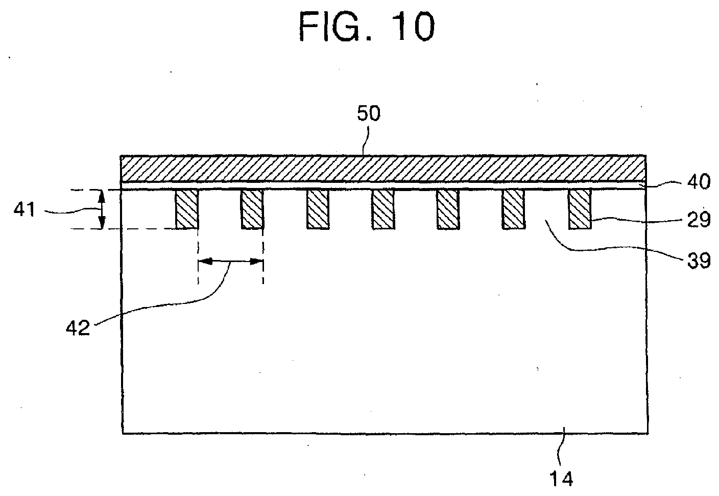
- a shape of the light scattering unit can be arbitrarily set according to the material employed in the light transmissive substrate or the light scattering unit. That is, as shown in Fig. 8, the surface of the light scattering unit 27 in the depth direction does not necessarily need to be formed vertically, so that it can have a sloped surface against the light transparent substrate surface, which is approximately flat. Further, as shown in Fig. 9, an interface between the light scattering unit 28 and the light transparent substrate 13 does not necessarily need to be flat, so that it can be uneven (prominence and depression). At this case, the unevenness can be formed to attribute to the scattering.
- the unevenness can be formed in this surface with dry etching method that uses atom-shaped boron formed by discharge or with wet etching method that uses etchant, such as HF, where those etching methods are used in manufacturing a semiconductor.
- the light transmissive substrate of the present invention can be formed with planarization layer 40 coating as shown in Fig. 10, when used in the organic electroluminescence element.
- the interval between the anode 50 and the light scattering layer 29 is as small as possible, so that the thickness of the planarization layer 40 is below 100nm, preferably.
- the length in the thickness direction of the light transparent substrate of the light scattering unit (in the normal direction of the substrate surface) can be arbitrarily set.
- the length in the thickness direction of the substrate of the light scattering unit 200 can be set so as to scatter the exit light 52 having an angle more than a critical angle of the interface between the light transmissive substrate 15 and air as shown in Fig. 11, for example.
- a height of the light scattering unit which is required for scattering the exit light having an angle more than the critical angle, can be set to the distance from the substrate surface of the light transparent substrate to the light-emitting center.
- one side of the light scattering units 20, 27, 28 is a surface (cross-sectional surface) of the light transparent substrate 10, 12, 13.
- the light scattering unit is buried within the light transparent substrate or that the end of the light scattering unit has the same position as the surface of the light transparent substrate, in order to obtain the substrate flatness.
- a method of manufacturing the substrate for the optical element comprising the light scattering unit and the light transparent unit used herein will be further described.
- this method there can be employed a method of forming a groove in the substrate and then burying light scattering material in the groove, or a method of depositing the light scattering material on the substrate and then covering it with the light transparent material (for forming the light transmissive opening).
- the known method for example, the conventional exposure process using photoresist, can be used.
- various photolithography processes can be used as a method of forming the groove in the pattern shape.
- Fig. 12 shows an exposure process using a mask 72, when forming such a groove.
- the exposure process using the mask 72 can arbitrarily design the ratio of a pitch or line to a space (groove, width, and groove interval) of a target groove.
- Fig. 13 is an example of forming a groove with a two-optical-flux interference exposure process of laser. It is possible for the two-optical-flux interference exposure process of the laser to perform exposure of a large area in a short time, and is especially effective to form the light scattering unit in the periodic configuration.
- the pitch can be simply set with any value more than 244nm, by simply adjusting the crossing angle.
- the laser light employed in the two-optical-flux interference exposure process randomly uses a light source, though not limited, such as solid laser, gas laser, semiconductor laser, and color laser, etc. to appropriately set the value d.
- a light source such as solid laser, gas laser, semiconductor laser, and color laser, etc.
- the laser light source When used in forming the diffraction grating included in the organic electroluminescence element, it is preferable to use the laser light source in the same range of wavelength as the visible light.
- the light source for use in this process is, for example, a YAG laser, a YAG laser multiple wave, a YAG laser triple wave, a color laser, a HE-Ne laser, a Ar ion laser, a Kr ion laser, a Cu vapor laser, a He-Cd laser, and N 2 laser, etc.
- the photoresist material for use in forming patterns can be appropriately selected among a positive type resist material, and a negative type resist material and the like.
- an etching process is performed to get a groove 90 shown in Fig. 15.
- This etching process can be selected among the known methods, such as wet etching, reactive ion etching, and ion milling, in order to form the groove.
- the light scattering material 91 can be filled only in the groove 90, and after forming a layer with the light scattering material 91 all over the substrate surface as shown in Fig. 16, the light scattering material 91 formed on the light transmissive portion by a polishing process (e.g. CMP process) can be removed.
- the light scattering material 91 can use a mixture that has different refractive index materials.
- the mixture can be either a solid/air mixture, such as porous SiO 2 layer, or a solid/solid mixture, such as SiO 2 /TiO 2 (the mixture can have a layer shape) layer.
- a solid/air mixture such as porous SiO 2 layer
- a solid/solid mixture such as SiO 2 /TiO 2 (the mixture can have a layer shape) layer.
- gas such as nitrogen, or liquid is also available, and it is preferable to have scattering characteristics.
- the organic electroluminescence element of the present invention comprises a substrate for an optical element, an anode, an organic layer made of at least emission layer, and a cathode.
- Figs. 17 and 18 show that organic layers 510, 530, 540 are stacked either one layer or stacked layer more than two layers between electrodes 520, 500, 501.
- the organic electroluminescence element of the present invention can be either a small molecular type or a high molecular type.
- the hole transport material used in the present invention is not specifically limited, and thus, if it is typically used as the hole transport material, any compound is acceptable.
- a specific example of the hole transport material there can be employed a triphenyl diamine group or a starburst molecule type, such as bis(di(P-trile)aminophenyl-1,1-cyclohexan, N-N'-diphenyl-N-N'-bis(3-methylphenyl)-1-1'-biphenyl-4-4'-diamine, N-N' diphenyl-N-N-bis(1-naphthyl)-1,1'-biphenyl)-4-4'-diamine.
- a triphenyl diamine group or a starburst molecule type such as bis(di(P-trile)aminophenyl-1,1-cyclohexan, N-N'-diphenyl-N-N'-bis(3-methylphenyl
- the electron transports material used in the present invention is not specifically limited, and thus, if it is typically used as the electron transport material, any compound is acceptable.
- the electron transport material there can be employed oxadiazol derivatives, triazol derivatives, quinolinol metal complex, such as 2-(4-biphenyl)-5-4(t-buthylphenyl)-1, 3, 4-oxadiazol, bis ⁇ 2-(4-t-buthylphenyl)-1,3,4-oxadiazol ⁇ -m-phenylene.
- the light-emitting material used in the present invention is not specifically limited, and thus, if it is typically used as the light-emitting material, any compound is acceptable.
- the light-emitting material there can be employed distyril-arylene derivatives (Japanese Patent Application Laid-Open Nos. H2-247278 and H5-17765), coumarin derivatives, dicyano-methylene-pyran derivatives and perylene derivatives (Japanese Patent Application No. S68-264692), aromatic ring system material (Japanese Patent Application Laid-Open Nos. H8-298186 and H9-268284), anthracene group (Japanese Patent Application Laid-Open Nos. H9-157643, H9-268283, and H10-72581), and quinacridone derivatives (Japanese Patent Application Laid-Open No. H5-70773).
- the anode of the organic electroluminescence plays a role injecting holes into the hole transport layer, and is effective that it has above 4.5eV work function.
- a specific example of anode material used in the present invention is ITO, NESA, gold, silver, platinum, and copper, etc.
- the cathode is to inject electrons into electron transport band or emission layer, preferably, it is a low work function material.
- the cathode material is not particularly limited, and specifically, there can be used In, Al, Mg, Mg-In alloy, Mg-Al alloy, Al-Li alloy, Al-Sc-Li alloy, and Mg-Ag alloy, etc.
- the organic electroluminescence element of the present invention can be used for passive drive, and for active drive by adding an active element, such as thin film transistors TFT.
- a method of forming each layer of the organic electroluminescence element of the present invention is not particularly limited, and can be selected among the known methods. For example, there can be employed vacuum deposition, molecular bean etching (MBE), or a method of dipping solvent or dispersion into solution or emulsion, spin coating, casting, bar coating, and roll coating.
- the organic electroluminescence display device of the present invention comprises a plurality of organic electroluminescence elements.
- the method of driving this display device can be either an active type or a passive type, and not particularly limited.
- Figs.19 and 20 Illustrate examples of an active matrix organic electroluminescence display device that comprises a substrate for an optical element.
- a light transparent substrate 600 having light emitting region and pixel driving circuit region is provided.
- a light scattering unit 650 and a light transmissive opening 651 may be formed in light emitting region of a light transparent substrate 600 as shown in Fig. 19.
- a light scattering unit 650 and a light transmissive opening 651 may be formed in light emitting region and pixel driving circuit region of a light transparent substrate 600 as shown in Fig. 20.
- the light scattering unit 650, the light transmissive opening 651 and the light transparent substrate 600 constitute a substrate for an optical element.
- a buffer layer 601 is formed on the substrate for an optical element.
- the substrate for an optical element has the same configuration as in the above-stated embodiment.
- a TFT and a capacitor 620 are formed on the buffer layer 601 of the pixel driving circuit region.
- the TFT comprises n or p type semiconductor layer 602; a gate insulating film 603 burying the semiconductor layer 602; a gate electrode 604 corresponding to the semiconductor layer 602; a first insulating layer 605 burying the gate electrode 604; a drain electrode 607a and a source electrode 607b.
- the drain electrode 607a and the source electrode 607b are connected to both sides of the semiconductor layer 602 via contact holes 606a and 606b, respectively, wherein the contact holes 606a and 606b are formed in the first insulating layer 605 and the gate insulating film 603.
- the capacitor 620 has a lower electrode 621 buried by the first insulting layer 605 and a upper electrode 622 opposing to the lower electrode 621, wherein the upper electrode 622 is connected to the source electrode 607b and formed on the first insulating layer 605.
- a second insulating layer 608 is formed on the first insulting layer 605.
- a first electrode layer 609 is formed on the second insulating layer 608 to electrically connect to the drain electrode 607a.
- a planarization film 610 having an opening exposing the first electrode layer 609 is formed. The opening is positioned on the light emitting region.
- An organic layer 611 is stacked on the first electrode layer 609.
- a second electrode layer 612 is formed on the organic layer 61 1and the planarization film 610.
- the bottom emitting organic electroluminescence display comprising the first electrode layer 609 formed of ITO being a transparent conductive material and comprising the light transparent substrate 600, the buffer layer 601, the gate insulting film 603, and the first and second insulating layers 605 and 608 each formed of a transparent material.
- the position where the light scattering unit 650 and the light transmissive opening 651 is to be formed is not limited to those embodiments and may be between layers with high refractive index.
- the light scattering unit 650 and the light transmissive opening 651 may be formed in light emitting region of a second insulting layer 608.
- a positive resist material was formed on the quartz substrate (refractive index: 1.457) in a thickness of 4000 ⁇ using a spin coater, as a photoresist material, and then the resist material was patterned using a photomask.
- an Hg-Xe lamp (wavelength: 250nm) was used.
- a stripe type mask pattern was used with a period of 1.0 ⁇ m, a line width of 0.75 ⁇ m, and a space width of 0.25 ⁇ m.
- the mask was rotated 90°, and was exposed again with the same condition. After such exposure, the mask was processed with alkali developer to form the resist pattern.
- a target grating pattern could be manufactured.
- the quartz substrate attached to the manufactured resist pattern was etched by reactive gas etching (Samuco, RIE1ONR). Etching was performed under the condition of 100W output, using CF 4 (4Pa, 20SCCM). The etching was performed to make a groove of 10000 ⁇ in the quartz substrate during 2080 seconds.
- the formed groove was processed with dilute hydrofluoric acid, and the unevenness was formed in the groove.
- dispersion used in the sol-gel process by which TiO 2 is formed, was applied to the formed groove, and the filling-up of TiO 2 was performed by the low temperature plastic sol-gel process.
- the substrate surface was flattened by polishing the substrate surface using the chemical-mechanical polishing (CMP) method. Measuring the flatness of the substrate surface, Ra was 2nm. This substrate showed good scattering characteristics by TiO 2 /quartz interface and TiO 2 itself.
- ITO was formed in a layer on the substrate using a sputtering process so that the sheet resistance becomes 20 ⁇ / ⁇ . An ITO layer was 100nm thick.
- N, N'-bis(3-methylpenyl)-N, N' -diphenyl -[1,1'-biphenyl]-4,4'-diamine was formed in a thickness of 50nm using the vacuum deposition method, and then tris(8-quinolinol)aluminum was formed as the emission layer in a thickness of 70nm using the vacuum deposition method.
- Mg-Ag alloy was deposited as the cathode in a thickness of 150nm, using the vacuum deposition method at a deposition speed ratio 9:1 (atom weight ratio) to manufacture the organic electroluminescence element.
- the luminous area was 4 mm 2 .
- an organic electroluminescence element was manufactured identical to that of the first example.
- a current of 5mA/cm 2 was applied to this device, a luminance of 190cd/m 2 was obtained.
- a positive resist material was formed on the quartz substrate (refractive index: 1.457) in a thickness of 4000 ⁇ by a spin coater, as a photoresist material, and then the formed photoresist layer was exposed by two-optical-flux laser interference exposure system.
- an Ar-ion laser (wavelength: 488nm) was employed to make exposure under the following conditions.
- Laser light was branched into 2 light flux with a beam splitter, and interference exposure was performed with a mirror such that a crossing angle becomes about 31 degree on the substrate surface (laser illumination intensity: 100mA/cm 2 , exposure time: 15 seconds). After such exposure was performed one time, the substrate was rotated 90° and exposed again with the same condition.
- the formed groove was processed by dilute hydrofluoric acid, and the unevenness was formed in the groove.
- the resist material was removed by a remover.
- the sol-gel process the groove is filled up and flattened using TiO 2 porous layer.
- TiO 2 was polished by the CMP process. By this polishing, the periodic structure of TiO 2 can be manufactured on the quartz substrate. Measuring the flatness of the substrate surface under the same conditions as the first example, Ra was 2nm. This substrate shows slight scattering characteristics through TiO 2 /quartz interface and TiO 2 itself.
- ITO is formed in a layer on the substrate using a sputtering process so that the sheet resistance becomes 20 ⁇ / ⁇ . An ITO layer was 100nm thick.
- N,N'-bis(3-methylpenyl)-N,N'-diphenyl -[1,1'-biphenyl]-4,4'-diamine was formed in a thickness of 50nm using the vacuum deposition method, and then tris(8-quinolinolat)aluminum was formed as the emission layer in a thickness of 70nm using the vacuum deposition method.
- Mg-Ag alloy was deposited as the cathode in a thickness of 150nm, using the vacuum deposition method at a deposition speed ratio 9:1 to manufacture the organic electroluminescence element.
- the luminous area was 4 mm 2 .
- a current of 5mA/cm 2 was applied to this device, a luminance of 275cd/m 2 was obtained.
- the luminance in the front direction of the substrate is improved, and the organic electroluminescence having good visibility can be provided
Abstract
Description
- This application claims the benefit of Japanese Patent Application No. 2003-282202, filed July 29, 2003, the disclosure of which is hereby incorporated herein by reference in its entirety.
- The present invention relates to a substrate for an optical element that emits light of a specific wavelength range by current driving, optical element using the same andorganic electroluminescence display device used as a display device.
- An organic electroluminescence (organic EL) device is an emissive device using a principle that a fluorescent material is emitted by recombination energy between holes injected from an anode and electrons injected from a cathode by applying the electric field. Since C.W. Tang, et al. reported a low voltage driven organic electroluminescence display with a stacked type device (C.W. Tang, S.A. VanSlyke, Applied Physics Letter, Vol. 51, p. 913, 1987), a research on the organic electroluminescence element made of organic material has widely conducted. Tang et al uses Tris(8-Qionolinol) Aluminum in an emission layer and triphenyldiamine derivatives in a hole transport layer.
- Advantages of the stacked structure are to increase hole injection efficiency toward the emission layer, to block electrons injected from the cathode to increase formation efficiency of an exciton formed by recombination, and to isolate the exciton formed in the emission layer, etc.
- As an organic electroluminescence element described above, a two-layer type having a hole transport (injection) layer and an electron transport emission layer, or a three-layer type having a hole transport (injection) layer, an emission layer, and an electron transport (injection) layer are widely known. For such a stacked type device, researches on structure and method of forming the device have been conducted in order to increase recombination efficiency between the injected hole and electron. However, the organic electroluminescence has a limit to the probability of forming a singlet due to dependency of spin statistics when recombining carriers, and thus having an upper limit in lumonous efficiency. This upper limit value is about 25%.
- Further, for a surface emitting device, such as an organic electroluminescence element, light that has an exit angle over a critical angle is totally reflected due to a refractive index of a luminous body, so that it cannot be emitted outward. Thus, it is expected that if the refractive index of the luminous body is set to 1.6, only 20% of the total amount of luminescence will be available. Therefore, the limit of the energy conversion efficiency is about 5 %, including the singlets formation probability, so that there cannot but be lower efficiency (cf. Tetsuo TSUTSUI, "Present status of research and development in organic electroluminescent devices" : Monthly Display, Vol. 1, No. 3, p11, September 9, 1995.). In an organic electroluminescence element having a strong limitation in luminous efficiency, light extraction efficiency undergoes fatal performance degradation.
- A method of increasing this light extraction efficiency has been investigated with regard to a light-emitting device having a structure, such as a conventional inorganic electroluminescence element. For example, a method of increasing efficiency by comprising a light-focusing property in the substrate (Japanese Patent Application Laid-Open No. S63-314795), or a method of forming a reflective surface on a side of a device (Japanese Patent Application Laid-Open No. H01-220394) have been proposed. Further, introducing a flat layer that has an intermediate refractive index between a substrate glass and a luminous body to form an anti-reflection film (Japanese Patent Application Laid-Open No. S62-172691) was also proposed.
- Further, Japanese Patent Application Laid-Open No. 2002-260844 discloses an organic electroluminescence element comprising a waveguide formed by a partition formed on a substrate adjacent to the pixel used herein, wherein the partition is formed of transparent polymer and white corpuscles, or this polymer and transparent corpuscles dispersed in the polymer, having a refractive index different from that of the polymer. (Referring to Fig. 2 and Claims of said application)
- Further, Japanese Patent Application Laid-Open No. 2002-260866 discloses an organic electroluminescence element comprising an anode that injects a hole, an emission layer having a luminous zone, and an cathode that injects an electron, and wherein at least one of these electrodes is transmissive, and this transmissive electrode includes a means for changing an angle of light emitted from the emission layer therein (Fig. 1, Detailed Description of the Invention, Paragraph 0026: Claim 1.)
- Further, Japanese Patent Application Laid-Open No. 2002-260845 discloses one or a plurality of organic electroluminescence elements having a substrate and a plurality of light converting means and formed directly on one surface of the substrate or over the sublayer, wherein each of the plurality of organic electroluminescence elements comprises a plurality of light angle changing means. This Laid-Open Publication described that the light angle changing means has a configuration such that the length direction of a shape of transparent material, opaque particles or air layers faces the thickness direction of the substrate. (Claim 8 in the above Publication)
- The conventional method has the following problems. The method for increasing light extraction efficiency by making the substrate have a light-focusing propertyor the method of forming a reflective surface on a side of the device is effective for a device with a large luminous area, however, in a device with a small pixel area such as a dot matrix display, it is difficult to form a lens for light-focusing property or the reflective surface on a side, etc.,. Further, in the organic electroluminescence element, a film thickness of an emission layer is below several µm, so that it is difficult to perform taper turning to form a reflective mirror on a side of a device with the current processing technology for fine , thereby significantly increasing cost.
- Meanwhile, a method of introducing the flat layer having an intermediate refractive index between a substrate glass and a luminous body to form an anti-reflection layer has an effect in improving light extraction efficiency, however, it is difficult to prevent total reflection with this method. Therefore, while the effect of increasing light extraction efficiency is valid for the inorganic electroluminescence having a large refractive index, it is not valid for the organic electroluminescence element having a small refractive index.
- Further, transmission light toward a metal electrode (cathode) surface in the organic electroluminescence layer has great transmission loss due to the metal electrode. Thus, to effectively extract the transmission light, there is a need to place a partition in short interval. Therefore, the invention disclosed in Japanese Patent Application Laid-Open No. 2002-260844 reduces the luminous area of a device, thus it does not have such great improvement.
- Further, in the invention disclosed in the Japanese Patent Application Laid-Open No. 2002-260866, the area where the electric field cannot be applied increases so that there is no great improvement just like the above invention.
- Further, in the invention disclosed in the Japanese Patent Application Laid-Open No. 2002-260845, light having an exit angle over the critical angle cannot be effectively extracted. Further, while Japanese Patent Application Laid-Open No. 2002-260845 describes that the performance is improved when the light angle changing means are distributed all over the substrate (Fig. 10 and Paragraph 0032 in the Description corresponding to Fig. 10 in this publication), however, there is a problem that if a plurality of scatters exist in the thickness direction, the substrate becomes white, thus reducing the color purity of the emitted light.
- As described above, the light extraction of the organic electroluminescence is still insufficient.
- The present invention is contrived to figure out how emitting light having an angle more than a critical angle and totally reflected at the air/glass interface can be effectively scattered to emit at an angle less than the critical angle.
- The present invention provides an optical element substrate (light emitting device substrate) that improves light extraction efficiency of an organic electroluminescence element.
- After reviewing the foregoing, the inventors found that light extraction efficiency is improved by using a substrate for an optical element comprising a light scattering unit that scatters visible light and a light transmissive opening that transmits the visible light in the light transparent substrate that transmits the visible light, as a light extraction substrate of an organic electroluminescence element. With this substrate for the optical element, a luminance of the organic electroluminescence element is increased.
- In other words, the substrate for the optical element of the present invention is characterized in that it comprises a light scattering unit that scatters visible light and a light transmissive opening that transmits the visible light in the light transparent substrate that transmits the visible light, and in that a length L of the light scattering unit in the thickness direction of the substrate and a width W of the light transmissive opening are found by the following Eq. 1.
- Specifically, it is preferable that one surface of the light scattering unit is the same as the surface of the light transparent substrate, and that the light transmissive opening, segmented by at least one light scattering unit, is formed in the light transparent substrate, and the light transmissive openings are periodically placed in a direction of substrate surface, and that the substrate for the optical element is to form at least one display pixel wherein the light scattering unit is extended in at least one direction in the display pixel.
- Further, it is preferable that the light scattering unit is a wall structure that segments the display pixel, and that the light transmissive opening formed by being segmented by the wall structure is periodically placed in the direction of substrate surface, and that the width W of the light transmissive opening is more than 100nm and less than 200 µm, and that the substrate for the optical element, in which the light transmissive openings are periodically placed in the direction of substrate surface, comprises a light scattering unit that scatters visible light and a light transmissive opening that transmits the visible light in one surface of the light transparent substrate that transmits the visible light, wherein the sum of the thickness of the segmented wall and the width of one adjacent light transmissive opening is more than 130nm and less than 25 µm, and that the light transmissive opening is isolated in a direction of substrate surface in the pixel.
- The organic electroluminescence element of the present invention comprises a substrate for an optical element of one of the above descriptions, at least an anode, an organic layer made of an emission layer, and a cathode.
- The organic electroluminescence display device of the present invention comprises a plurality of the organic electroluminescence element.
- The above and other features and advantages of the present invention will become more apparent to those of ordinary skill in the art by describing in detail preferred embodiments thereof with reference to the attached drawings in which:
- Figs. 1 and 2 are schematic cross-sectional views of a substrate for an optical element of the present invention;
- Figs. 3 to 7 are schematic plan views of a substrate of for an optical element of the present invention;
- Figs. 8 to 11 are schematic cross-sectional views of a substrate for an optical element of the present invention;
- Fig. 12 is a schematic cross-sectional view of a substrate, illustrating one process of manufacturing the substrate for an optical element of the present invention;
- Fig. 13 is a schematic view illustrating a process of manufacturing a substrate for an optical element of the present invention;
- Fig. 14 is a schematic cross-sectional view of a process of manufacturing a substrate for an optical element of the present invention;
- Figs. 15 and 16 are schematic views illustrating a process of manufacturing a substrate for an optical element of the present invention; and
- Figs. 17 and 18 are schematic cross-sectional views of an organic electroluminescence element using a substrate for an optical element of the present invention.
- Figs. 19 to 21 are schematic cross-sectional views Illustrating examples of an active matrix organic electroluminescence display device that comprises a substrate for an optical element.
-
- The present invention will now be described more fully hereinafter with reference to the accompanying drawings, in which preferred embodiments of the invention are shown. This invention may, however, be embodied in different forms and should not be construed as limited to the embodiments set forth herein. Rather, these embodiments are provided so that this disclosure will be thorough and complete, and will fully convey the scope of the invention to those skilled in the art. In the drawings, the thickness of layers and regions are exaggerated for clarity. Like numbers refer to like elements throughout the specification.
- Fig. 1 is a schematic cross-sectional view illustrating a substrate for an optical element of the present invention.
- As shown in Fig. 1, the substrate for the optical element of the present invention comprises a
light scattering unit 20 that scatters visible light and alight transmissive opening 30 that transmits the visible light, within a lighttransparent substrate 10 that transmits the visible light. Further, Fig. 1 shows a cross-sectional view cut in a direction perpendicular to the substrate surface. For the direction of the substrate surface, it is preferable that the substrate has the shape illustrated in Figs. 3 to 7. Further, Figs. 3 to 7 are just illustrations, and not limited to these shapes, thus the present invention can be formed such that eachlight scattering unit 22 to 26 or eachlight transmissive opening 32 to 36 are isolated in the direction of the substrate surface, - Since the light
transparent substrate 10 of the present invention serves as an optical element, it is necessary to be at least optically transparent when in use. That is, the lighttransparent substrate 10 of the present invention that transmits visible light can transmit at least some of the light whose wavelength is within 400 to 800nm, and can be formed of either inorganic or organic material. For example, the inorganic material used for this substrate can be glass, and the organic material can be plastic, etc. - Preferable, the plastic described above can employ engineering plastic, such as Polyethersulfone (PES), Polyethylene Terephthalate (PET), or its derivates. Further, the substrate can employ a plurality of different materials, which can be either among inorganic materials, or among organic materials, or even a mixture between inorganic and organic materials. The substrate can also be formed in a film shape using one or a plurality of materials (a plurality of organic mixtures, inorganic mixtures, and organic and inorganic mixtures), and can also be formed by coating the fabricated film a plurality of times.
- For the light
transparent substrate 10 of the present invention, preferably, thelight transmissive opening 20 is isolated in the direction of the substrate surface, and more preferably, in the direction of one substrate surface (in the direction of one surface of the substrate) as illustrated in Figs. 1, 2, 8, 9, 10, 17 and 18. That is, in the present invention, thelight transmissive openings light scattering units light transmissive openings substrate 10, where "optically same" means that light within a wavelength (or any wavelength) has the same refractive index. - The
light scattering unit 20 of the present invention scatters at least some light having a wavelength of 400 to 800nm. Thelight scattering unit 20 can be made of inorganic or organic material. Further, it can be made of one or a plurality of components. Further, thelight transmissive opening 30 of the present invention indicates a transparent portion observed in the normal direction of the surface of the light transmissive substrate 10 (in the direction perpendicular to the screen when used as a display). As such, the substrate for the optical element of the present invention is not such a structure that the light scattering unit (the film, if the light scattering unit is formed in a film type) covers all over the substrate surface. For the substrate for the optical element, light from the electrode of the organic electroluminescence element transmitted in the horizontal direction (light that has a large component in the direction of substrate surface) is efficiently scattered, thus improving the luminance in the front direction of the substrate. - To describe the present invention in more detail, in the light transparent substrate of the present invention, the
light scattering unit 20 and thelight transmissive opening 30 are placed (optically) alternatively in the direction of the substrate surface. That is, seen in the normal direction of the surface of the light transmissive substrate (in the direction perpendicular to the substrate surface), thelight scattering unit 20 and thelight transmissive opening 30 are placed alternatively in the direction of the substrate surface (in the direction of one side of the substrate surface). - Although the alternative placements do not necessarily need to be periodic, it is preferable that the
light scattering unit 20 and thelight transmissive opening 30 are periodically placed in the direction of the substrate surface, preferably, in the surface direction of one side of substrate surface (one side surface) due to the design or manufacture convenience. Such a period can be set arbitrarily, however, when the length is a reference, it is preferable that the sum of the thickness of the segmented wall and the width of one adjacentlight transmissive opening 30 is 130nm to 25 µm. - Further, this period can be plural in the substrate surface. The period can vary according to a place, or according to a direction of the substrate surface. Further, the width of the
light transmissive opening 30 is 100 nm to 20 µm, and preferably, 110 nm to 10 µm. - Referring to Fig. 3, the configuration of the light scattering unit that scatters the visible light used in the present invention will now be described. The configuration of the light scattering units can be a
stripe type 22 shown in Fig. 3, adot type wall type - That is, when the light transmissive opening is formed in the light transmissive substrate, segmented by at least one light scattering unit, any pattern is acceptable. The specific configuration is not limited to the detailed examples illustrated in the embodiments. Particularly, as shown in Figs. 3 or 6, it is preferable that the
light scattering unit light scattering unit 22 is extended in one-axis direction. Further, Fig. 6 shows that thelight scattering unit 25 is crossed in the extended one-axis direction. As shown in Fig. 6, a shape of one pixel segmented by being crossed in the display pixel can be formed in polygon (a rectangle: square (regular square, for example) or a regular polygon: regular pentagon, regular hexagon). Preferably, the segmented one pixel is formed segmented with the pixel adjacent to the wall structure. Preferably, for the substrate of the present invention, this segmented pixel (or its group) has a period in the direction of substrate surface as shown in Figs. 3, 6 and 7. Further, as described above, while this period can be arbitrarily set, it is preferable that, when the length is a reference, the sum of the thickness of the segmented wall and the width of one adjacent light transmissive opening is 130nm to 25 µm. Further, there can be a plurality of periods within the substrate surface. The periods can vary according to a place or a direction of the substrate surface. Preferably, the width of the light transmissive opening is 100nm to 20 µm, and more preferably, 100nm to 10 µm. - Further, a shape of the light scattering unit can be arbitrarily set according to the material employed in the light transmissive substrate or the light scattering unit. That is, as shown in Fig. 8, the surface of the
light scattering unit 27 in the depth direction does not necessarily need to be formed vertically, so that it can have a sloped surface against the light transparent substrate surface, which is approximately flat. Further, as shown in Fig. 9, an interface between thelight scattering unit 28 and the lighttransparent substrate 13 does not necessarily need to be flat, so that it can be uneven (prominence and depression). At this case, the unevenness can be formed to attribute to the scattering. For example, the unevenness can be formed in this surface with dry etching method that uses atom-shaped boron formed by discharge or with wet etching method that uses etchant, such as HF, where those etching methods are used in manufacturing a semiconductor. Further, the light transmissive substrate of the present invention can be formed withplanarization layer 40 coating as shown in Fig. 10, when used in the organic electroluminescence element. Here, it is preferable that the interval between theanode 50 and thelight scattering layer 29 is as small as possible, so that the thickness of theplanarization layer 40 is below 100nm, preferably. - The length in the thickness direction of the light transparent substrate of the light scattering unit (in the normal direction of the substrate surface) can be arbitrarily set. To improve the light extraction efficiency of such an organic electroluminescence element, the length in the thickness direction of the substrate of the
light scattering unit 200 can be set so as to scatter theexit light 52 having an angle more than a critical angle of the interface between thelight transmissive substrate 15 and air as shown in Fig. 11, for example. At this case, the critical angle depends on the refractive index of air and that of thelight transmissive substrate 15, and their relationship can be represented as c=arcsin(n1/n2), where n1 and n2 indicate the refractive index of air and that of thelight transmissive substrate 15, respectively. Further, it is preferable that they have a relationship expressed as W/Lan(arcsin(n1/n2)) in Eq. 1, where "L" indicates the thickness 41 (length in the substrate direction), and "W" indicates the size of the light transparent opening (light transmissive opening). Further, in Figs. 8 and 9, "L" indicates the length in the thickness direction of the substrate of the light scattering units 27and 28 and "W" indicates the width of the lighttransmissive openings 37and 38. Further, a height of the light scattering unit, which is required for scattering the exit light having an angle more than the critical angle, can be set to the distance from the substrate surface of the light transparent substrate to the light-emitting center. Particularly, as shown in Figs. 1, 8 and 9, it is preferable that one side of thelight scattering units transparent substrate - When the organic electroluminescence element is formed on the substrate for the optical element of the present invention, it is preferable that the light scattering unit is buried within the light transparent substrate or that the end of the light scattering unit has the same position as the surface of the light transparent substrate, in order to obtain the substrate flatness.
- A method of manufacturing the substrate for the optical element comprising the light scattering unit and the light transparent unit used herein will be further described. As this method, there can be employed a method of forming a groove in the substrate and then burying light scattering material in the groove, or a method of depositing the light scattering material on the substrate and then covering it with the light transparent material (for forming the light transmissive opening).
- When the method of forming the groove in the pattern shape is employed as the method of forming the groove, the known method, for example, the conventional exposure process using photoresist, can be used. Further, various photolithography processes can be used as a method of forming the groove in the pattern shape.
- Fig. 12 shows an exposure process using a
mask 72, when forming such a groove. The exposure process using themask 72 can arbitrarily design the ratio of a pitch or line to a space (groove, width, and groove interval) of a target groove. - Fig. 13 is an example of forming a groove with a two-optical-flux interference exposure process of laser. It is possible for the two-optical-flux interference exposure process of the laser to perform exposure of a large area in a short time, and is especially effective to form the light scattering unit in the periodic configuration. For this method, the pitch d of the periodic configuration has the following relationship: d=(λ/2)/[sin(/2)], where "λ" indicates a laser wavelength used in this exposure, and "" indicates a crossing angle of the 2 light flux of the laser for irradiating a
photoresist material 74 on the substrate. As gets larger, d becomes smaller, and when the crossing angle is 180°, d becomes λ/2 of the minimum value. For example, when a laser of 488nm (λ) is irradiated using an argon-ion laser, d〉 244nm. That is, the pitch can be simply set with any value more than 244nm, by simply adjusting the crossing angle. - The laser light employed in the two-optical-flux interference exposure process randomly uses a light source, though not limited, such as solid laser, gas laser, semiconductor laser, and color laser, etc. to appropriately set the value d.
- When used in forming the diffraction grating included in the organic electroluminescence element, it is preferable to use the laser light source in the same range of wavelength as the visible light. For this, the light source for use in this process is, for example, a YAG laser, a YAG laser multiple wave, a YAG laser triple wave, a color laser, a HE-Ne laser, a Ar ion laser, a Kr ion laser, a Cu vapor laser, a He-Cd laser, and N2 laser, etc.
- The photoresist material for use in forming patterns can be appropriately selected among a positive type resist material, and a negative type resist material and the like. After forming the pattern in the
photoresist material 74 shown in Fig. 14, an etching process is performed to get agroove 90 shown in Fig. 15. This etching process can be selected among the known methods, such as wet etching, reactive ion etching, and ion milling, in order to form the groove. - Subsequently, a method of filling the
groove 90 with thelight scattering material 91 will now be described. For this method, there can be employed either a wet process, such as sol-gel process, or a vacuum process, such as sputtering, deposition or CVD process. Here, thelight scattering material 91 can be filled only in thegroove 90, and after forming a layer with thelight scattering material 91 all over the substrate surface as shown in Fig. 16, thelight scattering material 91 formed on the light transmissive portion by a polishing process (e.g. CMP process) can be removed. Thelight scattering material 91 can use a mixture that has different refractive index materials. The mixture can be either a solid/air mixture, such as porous SiO2 layer, or a solid/solid mixture, such as SiO2/TiO2 (the mixture can have a layer shape) layer. Meanwhile, when the wall of thegroove 90 is uneven, thelight scattering material 91 is not necessarily needed, and when filled, a solid material is preferable as a filling material. However, gas, such as nitrogen, or liquid is also available, and it is preferable to have scattering characteristics. - The organic electroluminescence element of the present invention comprises a substrate for an optical element, an anode, an organic layer made of at least emission layer, and a cathode. As a specific example of the device configuration of the organic electroluminescence element according to the present invention, Figs. 17 and 18 show that
organic layers electrodes - The hole transport material used in the present invention is not specifically limited, and thus, if it is typically used as the hole transport material, any compound is acceptable. As a specific example of the hole transport material, there can be employed a triphenyl diamine group or a starburst molecule type, such as bis(di(P-trile)aminophenyl-1,1-cyclohexan, N-N'-diphenyl-N-N'-bis(3-methylphenyl)-1-1'-biphenyl-4-4'-diamine, N-N' diphenyl-N-N-bis(1-naphthyl)-1,1'-biphenyl)-4-4'-diamine.
- The electron transports material used in the present invention is not specifically limited, and thus, if it is typically used as the electron transport material, any compound is acceptable. As a specific example of the electron transport material, there can be employed oxadiazol derivatives, triazol derivatives, quinolinol metal complex, such as 2-(4-biphenyl)-5-4(t-buthylphenyl)-1, 3, 4-oxadiazol, bis{2-(4-t-buthylphenyl)-1,3,4-oxadiazol}-m-phenylene.
- The light-emitting material used in the present invention is not specifically limited, and thus, if it is typically used as the light-emitting material, any compound is acceptable. As a specific example of the light-emitting material, there can be employed distyril-arylene derivatives (Japanese Patent Application Laid-Open Nos. H2-247278 and H5-17765), coumarin derivatives, dicyano-methylene-pyran derivatives and perylene derivatives (Japanese Patent Application No. S68-264692), aromatic ring system material (Japanese Patent Application Laid-Open Nos. H8-298186 and H9-268284), anthracene group (Japanese Patent Application Laid-Open Nos. H9-157643, H9-268283, and H10-72581), and quinacridone derivatives (Japanese Patent Application Laid-Open No. H5-70773).
- The anode of the organic electroluminescence plays a role injecting holes into the hole transport layer, and is effective that it has above 4.5eV work function. A specific example of anode material used in the present invention is ITO, NESA, gold, silver, platinum, and copper, etc. Further, the cathode is to inject electrons into electron transport band or emission layer, preferably, it is a low work function material. The cathode material is not particularly limited, and specifically, there can be used In, Al, Mg, Mg-In alloy, Mg-Al alloy, Al-Li alloy, Al-Sc-Li alloy, and Mg-Ag alloy, etc. Further, the organic electroluminescence element of the present invention can be used for passive drive, and for active drive by adding an active element, such as thin film transistors TFT. A method of forming each layer of the organic electroluminescence element of the present invention is not particularly limited, and can be selected among the known methods. For example, there can be employed vacuum deposition, molecular bean etching (MBE), or a method of dipping solvent or dispersion into solution or emulsion, spin coating, casting, bar coating, and roll coating.
- Further, the organic electroluminescence display device of the present invention comprises a plurality of organic electroluminescence elements. The method of driving this display device can be either an active type or a passive type, and not particularly limited.
- Figs.19 and 20 Illustrate examples of an active matrix organic electroluminescence display device that comprises a substrate for an optical element.
- Referring to Fig.19 and 20, a light
transparent substrate 600 having light emitting region and pixel driving circuit region is provided. Alight scattering unit 650 and alight transmissive opening 651 may be formed in light emitting region of a lighttransparent substrate 600 as shown in Fig. 19. On the other hand, alight scattering unit 650 and alight transmissive opening 651 may be formed in light emitting region and pixel driving circuit region of a lighttransparent substrate 600 as shown in Fig. 20. Thelight scattering unit 650, thelight transmissive opening 651 and the lighttransparent substrate 600 constitute a substrate for an optical element. Abuffer layer 601 is formed on the substrate for an optical element. The substrate for an optical element has the same configuration as in the above-stated embodiment. - A TFT and a
capacitor 620 are formed on thebuffer layer 601 of the pixel driving circuit region. The TFT comprises n or ptype semiconductor layer 602; agate insulating film 603 burying thesemiconductor layer 602; agate electrode 604 corresponding to thesemiconductor layer 602; a first insulatinglayer 605 burying thegate electrode 604; adrain electrode 607a and asource electrode 607b. Thedrain electrode 607a and thesource electrode 607b are connected to both sides of thesemiconductor layer 602 viacontact holes contact holes layer 605 and thegate insulating film 603. Thecapacitor 620 has alower electrode 621 buried by the firstinsulting layer 605 and aupper electrode 622 opposing to thelower electrode 621, wherein theupper electrode 622 is connected to thesource electrode 607b and formed on the first insulatinglayer 605. - A second insulating
layer 608 is formed on the firstinsulting layer 605. Afirst electrode layer 609 is formed on the second insulatinglayer 608 to electrically connect to thedrain electrode 607a. Aplanarization film 610 having an opening exposing thefirst electrode layer 609 is formed. The opening is positioned on the light emitting region. Anorganic layer 611 is stacked on thefirst electrode layer 609. Asecond electrode layer 612 is formed on the organic layer 61 1and theplanarization film 610. - Meanwhile, in the bottom emitting organic electroluminescence display comprising the
first electrode layer 609 formed of ITO being a transparent conductive material and comprising the lighttransparent substrate 600, thebuffer layer 601, the gateinsulting film 603, and the first and second insulatinglayers - At this time, the position where the
light scattering unit 650 and thelight transmissive opening 651 is to be formed is not limited to those embodiments and may be between layers with high refractive index. For example, thelight scattering unit 650 and thelight transmissive opening 651 may be formed in light emitting region of a secondinsulting layer 608. - Examples of the present invention will now be described in more detail. However, the present invention is not limited to these examples, and the specific scope is described with reference to the other parts of detailed description and accompanying drawings. Further, in the example of the present invention, measurement of luminescence characteristics of the organic electroluminescence element is performed at a light-focusing angle of 0.1 degree using a photometer TOPCON BM-5A placed in the normal direction of the substrate.
- A positive resist material was formed on the quartz substrate (refractive index: 1.457) in a thickness of 4000 Å using a spin coater, as a photoresist material, and then the resist material was patterned using a photomask.
- As a light source, an Hg-Xe lamp (wavelength: 250nm) was used. Here, a stripe type mask pattern was used with a period of 1.0 µm, a line width of 0.75 µm, and a space width of 0.25 µm. With this mask, after exposed one time, the mask was rotated 90°, and was exposed again with the same condition. After such exposure, the mask was processed with alkali developer to form the resist pattern. As a result of SEM observation, it was confirmed that a target grating pattern could be manufactured. The quartz substrate attached to the manufactured resist pattern was etched by reactive gas etching (Samuco, RIE1ONR). Etching was performed under the condition of 100W output, using CF4(4Pa, 20SCCM). The etching was performed to make a groove of 10000 Å in the quartz substrate during 2080 seconds.
- Subsequently, the formed groove was processed with dilute hydrofluoric acid, and the unevenness was formed in the groove. After removing the resist material with a remover, dispersion used in the sol-gel process, by which TiO2 is formed, was applied to the formed groove, and the filling-up of TiO2 was performed by the low temperature plastic sol-gel process. Subsequently, the substrate surface was flattened by polishing the substrate surface using the chemical-mechanical polishing (CMP) method. Measuring the flatness of the substrate surface, Ra was 2nm. This substrate showed good scattering characteristics by TiO2/quartz interface and TiO2 itself. ITO was formed in a layer on the substrate using a sputtering process so that the sheet resistance becomes 20Ω/□. An ITO layer was 100nm thick.
- Subsequently, the following two layers were formed as an organic layer on the formed ITO. First, as a hole transport layer, N, N'-bis(3-methylpenyl)-N, N' -diphenyl -[1,1'-biphenyl]-4,4'-diamine was formed in a thickness of 50nm using the vacuum deposition method, and then tris(8-quinolinol)aluminum was formed as the emission layer in a thickness of 70nm using the vacuum deposition method. Next, Mg-Ag alloy was deposited as the cathode in a thickness of 150nm, using the vacuum deposition method at a deposition speed ratio 9:1 (atom weight ratio) to manufacture the organic electroluminescence element. The luminous area was 4 mm2.
- When a current of 5mA/cm2 was applied to this manufactured device, a luminance of 275cd/m2 was obtained. It was confirmed that the luminous efficiency was improved compared to the organic EL device of the first comparative embodiment.
- Except for not having the light scattering unit, an organic electroluminescence element was manufactured identical to that of the first example. When a current of 5mA/cm2 was applied to this device, a luminance of 190cd/m2 was obtained.
- A positive resist material was formed on the quartz substrate (refractive index: 1.457) in a thickness of 4000 Å by a spin coater, as a photoresist material, and then the formed photoresist layer was exposed by two-optical-flux laser interference exposure system. As a laser light source used in this two-optical-flux laser interference exposure, an Ar-ion laser (wavelength: 488nm) was employed to make exposure under the following conditions.
- Laser light was branched into 2 light flux with a beam splitter, and interference exposure was performed with a mirror such that a crossing angle becomes about 31 degree on the substrate surface (laser illumination intensity: 100mA/cm2, exposure time: 15 seconds). After such exposure was performed one time, the substrate was rotated 90° and exposed again with the same condition.
- After exposure, it was processed by alkali developer AZ300MIF (manufactured by Clariant Japan Co.) to form the grating pattern. As a result of SEM observation, the periodic structure in about 475 nm was obtained. A ratio of a line to a space (ratio of pattern interval to pattern width) was almost 3 to 1. The quartz substrate attached to the manufactured resist pattern was etched using the reactive gas etching (Samuco, RIE-1ONR) process. The etching was performed under the condition of 100W output, using CF4(4Pa, 20SCCM). The groove was etched to 5000 Å in the quartz substrate during 1040 seconds. Subsequently, the formed groove was processed by dilute hydrofluoric acid, and the unevenness was formed in the groove. Next, the resist material was removed by a remover. Further, by the sol-gel process, the groove is filled up and flattened using TiO2 porous layer. Subsequently, TiO2 was polished by the CMP process. By this polishing, the periodic structure of TiO2 can be manufactured on the quartz substrate. Measuring the flatness of the substrate surface under the same conditions as the first example, Ra was 2nm. This substrate shows slight scattering characteristics through TiO2/quartz interface and TiO2 itself. ITO is formed in a layer on the substrate using a sputtering process so that the sheet resistance becomes 20Ω/□. An ITO layer was 100nm thick.
- Subsequently, two layers were formed as an organic layer on the formed ITO. First, as a hole transport layer, N,N'-bis(3-methylpenyl)-N,N'-diphenyl -[1,1'-biphenyl]-4,4'-diamine was formed in a thickness of 50nm using the vacuum deposition method, and then tris(8-quinolinolat)aluminum was formed as the emission layer in a thickness of 70nm using the vacuum deposition method. Next, Mg-Ag alloy was deposited as the cathode in a thickness of 150nm, using the vacuum deposition method at a deposition speed ratio 9:1 to manufacture the organic electroluminescence element. The luminous area was 4 mm2. When a current of 5mA/cm2 was applied to this device, a luminance of 275cd/m2 was obtained. As described above, according to the substrate of the present invention, the luminance in the front direction of the substrate is improved, and the organic electroluminescence having good visibility can be provided
Claims (10)
- A substrate for an optical element comprising
a light scattering unit that scatters visible light, and a light transmissive opening that transmits the visible light in a light transparent substrate transmitting the visible light;
wherein a length L of the light scattering unit in a thickness direction of the substrate and a width W of the light transmissive opening is found by the following equation: - The substrate according to claim 1,
wherein the one surface of the light scattering unit has the same surface as the light transparent substrate. - The substrate according to claim 1,
wherein the light transmissive opening is formed in the light transparent substrate, by being segmented by at least the light scattering unit, and
wherein the light transmissive opening is periodically placed in a direction of the substrate surface. - The substrate according to claim, wherein the substrate for the optical element is for forming at least one display pixel, and the light scattering unit is extended in at least one direction in the display pixel.
- The substrate according to claim 4, wherein the light scattering unit is a wall structure that segments the display pixel.
- The substrate according to claim 5, wherein the light transmissive opening segmented by the wall type structure is periodically placed in the direction of the substrate surface.
- The substrate according to claim 1, wherein the width W of the light transmissive opening is 100nm to 20 µm.
- The substrate according to claim 3, wherein the light transmissive opening is periodically placed in the direction of the substrate surface, and the sum of the thickness of the segmenting wall and the width of one light transmissive opening adjacent to the segmenting wall is 130nm to 25 µm.
- An organic electroluminescence element comprising the substrate for an optical element of the claim 1, an anode, an organic layer made of at least an emission layer, and a cathode.
- An organic electroluminescence display comprising a plurality of the organic electroluminescence element of the claim 9.
Applications Claiming Priority (2)
| Application Number | Priority Date | Filing Date | Title |
|---|---|---|---|
| JP2003282202A JP2005050708A (en) | 2003-07-29 | 2003-07-29 | Substrate for optical elements and organic electroluminescence element as well as organic electroluminescence display device |
| JP2003282202 | 2003-07-29 |
Publications (3)
| Publication Number | Publication Date |
|---|---|
| EP1503438A2 true EP1503438A2 (en) | 2005-02-02 |
| EP1503438A3 EP1503438A3 (en) | 2007-04-25 |
| EP1503438B1 EP1503438B1 (en) | 2012-11-07 |
Family
ID=33535671
Family Applications (1)
| Application Number | Title | Priority Date | Filing Date |
|---|---|---|---|
| EP04090293A Active EP1503438B1 (en) | 2003-07-29 | 2004-07-22 | Substrate for optical element, organic electroluminescence element and organic electoluminescence display device |
Country Status (5)
| Country | Link |
|---|---|
| US (1) | US7345419B2 (en) |
| EP (1) | EP1503438B1 (en) |
| JP (1) | JP2005050708A (en) |
| KR (1) | KR100623685B1 (en) |
| CN (1) | CN100416887C (en) |
Cited By (4)
| Publication number | Priority date | Publication date | Assignee | Title |
|---|---|---|---|---|
| GB2462433A (en) * | 2008-08-05 | 2010-02-10 | Cambridge Display Tech Ltd | Organic electroluminescent diode |
| JP2013235233A (en) * | 2012-05-09 | 2013-11-21 | Samsung Display Co Ltd | Methods of manufacturing optical sheets, organic light emitting display devices, and methods of manufacturing organic light emitting display devices |
| EP2648240A3 (en) * | 2012-04-06 | 2016-07-27 | Corning Precision Materials Co., Ltd. | Substrate for organic light-emitting device with enhanced light extraction efficiency, method of manufacturing the same and organic light-emitting device having the same |
| EP3491449A4 (en) * | 2017-04-05 | 2020-04-15 | Facebook Technologies, LLC | Corrective optics for reducing fixed pattern noise in head mounted displays |
Families Citing this family (43)
| Publication number | Priority date | Publication date | Assignee | Title |
|---|---|---|---|---|
| JP3838964B2 (en) * | 2002-03-13 | 2006-10-25 | 株式会社リコー | Functional element substrate manufacturing equipment |
| US7000207B2 (en) * | 2003-04-10 | 2006-02-14 | Sioptical, Inc. | Method of using a Manhattan layout to realize non-Manhattan shaped optical structures |
| JP4522760B2 (en) * | 2003-06-30 | 2010-08-11 | 株式会社半導体エネルギー研究所 | Light emitting device and method for manufacturing light emitting device |
| US7227306B2 (en) * | 2003-08-28 | 2007-06-05 | Samsung Sdi Co., Ltd. | Organic electroluminescence display having recessed electrode structure |
| KR100852110B1 (en) * | 2004-06-26 | 2008-08-13 | 삼성에스디아이 주식회사 | An organic electroluminescent display device and method for preparing the same |
| JP2006100430A (en) * | 2004-09-28 | 2006-04-13 | Toshiba Matsushita Display Technology Co Ltd | Organic el display |
| US20070145386A1 (en) * | 2004-12-08 | 2007-06-28 | Samsung Electro-Mechanics Co., Ltd. | Semiconductor light emitting device and method of manufacturing the same |
| KR100624449B1 (en) * | 2004-12-08 | 2006-09-18 | 삼성전기주식회사 | Semiconductor emitting device with approved and manufacturing method for the same |
| US20080176041A1 (en) * | 2005-03-10 | 2008-07-24 | Konica Minolta Holdings, Inc | Resin Film Substrate for Organic Electroluminescence and Organic Electroluminescence Device |
| JP2006331694A (en) * | 2005-05-23 | 2006-12-07 | Matsushita Electric Works Ltd | Organic light emitting element and substrate for the same |
| US7586245B2 (en) * | 2005-08-29 | 2009-09-08 | Osram Opto Semiconductors Gmbh | Using prismatic microstructured films for image blending in OLEDS |
| JP2007095326A (en) * | 2005-09-27 | 2007-04-12 | Dainippon Printing Co Ltd | Organic el display and method of manufacturing same |
| US7321193B2 (en) * | 2005-10-31 | 2008-01-22 | Osram Opto Semiconductors Gmbh | Device structure for OLED light device having multi element light extraction and luminescence conversion layer |
| US7420323B2 (en) * | 2005-10-31 | 2008-09-02 | Osram Opto Semiconductors Gmbh | Electroluminescent apparatus having a structured luminescence conversion layer |
| US8330348B2 (en) * | 2005-10-31 | 2012-12-11 | Osram Opto Semiconductors Gmbh | Structured luminescence conversion layer |
| KR100781613B1 (en) * | 2006-01-19 | 2007-12-05 | 네오뷰코오롱 주식회사 | Image display device, OLED and its manufacturing method |
| EP1830422A3 (en) | 2006-03-03 | 2012-03-07 | Semiconductor Energy Laboratory Co., Ltd. | Light emitting device and electronic device |
| JP4950673B2 (en) * | 2007-01-10 | 2012-06-13 | キヤノン株式会社 | Organic EL display device |
| US20090015142A1 (en) * | 2007-07-13 | 2009-01-15 | 3M Innovative Properties Company | Light extraction film for organic light emitting diode display devices |
| US8179034B2 (en) * | 2007-07-13 | 2012-05-15 | 3M Innovative Properties Company | Light extraction film for organic light emitting diode display and lighting devices |
| JP5090227B2 (en) * | 2008-03-26 | 2012-12-05 | 学校法人金沢工業大学 | Organic electroluminescence element, lighting device and display device |
| JP2009237113A (en) * | 2008-03-26 | 2009-10-15 | Dainippon Printing Co Ltd | Optical sheet and display device |
| WO2009119889A1 (en) * | 2008-03-28 | 2009-10-01 | 住友化学株式会社 | Organic electroluminescent device |
| JP5240839B2 (en) | 2008-08-22 | 2013-07-17 | Necライティング株式会社 | Surface light emitting device, illumination device including the same, and display device |
| US20100110551A1 (en) * | 2008-10-31 | 2010-05-06 | 3M Innovative Properties Company | Light extraction film with high index backfill layer and passivation layer |
| US7957621B2 (en) * | 2008-12-17 | 2011-06-07 | 3M Innovative Properties Company | Light extraction film with nanoparticle coatings |
| KR101147421B1 (en) * | 2009-11-26 | 2012-05-22 | 삼성모바일디스플레이주식회사 | Organic light emitting diode display |
| JP6062636B2 (en) * | 2011-03-10 | 2017-01-18 | ローム株式会社 | Organic EL device |
| KR101871803B1 (en) * | 2011-09-06 | 2018-06-29 | 한국전자통신연구원 | Organic light emitting diode and manufacturing method of the same |
| KR20130100629A (en) | 2012-03-02 | 2013-09-11 | 삼성디스플레이 주식회사 | Organic light emitting display device |
| US8921841B2 (en) * | 2012-05-09 | 2014-12-30 | Samsung Corning Precision Materials Co., Ltd. | Porous glass substrate for displays and method of manufacturing the same |
| KR102014827B1 (en) | 2012-06-12 | 2019-08-28 | 삼성디스플레이 주식회사 | Optical film and organic light emitting display device including the same |
| CN103633109B (en) * | 2012-08-29 | 2016-05-25 | 固安翌光科技有限公司 | There is organic elctroluminescent device of high light extraction efficiency and preparation method thereof |
| JP5974910B2 (en) * | 2013-01-18 | 2016-08-23 | ソニー株式会社 | Display panel and display device |
| JP6429465B2 (en) | 2013-03-07 | 2018-11-28 | 株式会社半導体エネルギー研究所 | Apparatus and manufacturing method thereof |
| WO2014196053A1 (en) * | 2013-06-06 | 2014-12-11 | パイオニア株式会社 | Light scattering film, light emitting element, light scattering film manufacturing method, and light emitting element manufacturing method |
| KR102295537B1 (en) * | 2014-09-30 | 2021-08-31 | 삼성디스플레이 주식회사 | Organic light-emitting display apparatus |
| KR102370035B1 (en) * | 2015-02-05 | 2022-03-07 | 삼성디스플레이 주식회사 | Transparent display substrates, transparent display devices and methods of manufacturing transparent display devices |
| JP6401650B2 (en) | 2015-03-31 | 2018-10-10 | 住友化学株式会社 | OLED display device and manufacturing method thereof |
| DE102016122901A1 (en) * | 2016-11-28 | 2018-05-30 | Osram Oled Gmbh | Optoelectronic component and method for producing an optoelectronic component |
| CN108807714A (en) * | 2017-05-04 | 2018-11-13 | 中华映管股份有限公司 | The formed method of light-extraction layer and organic LED structure |
| CN108565351B (en) * | 2018-04-17 | 2019-12-24 | 深圳市华星光电技术有限公司 | OLED display device and manufacturing method thereof |
| CN112447926A (en) * | 2019-09-03 | 2021-03-05 | 群创光电股份有限公司 | Display device and electronic apparatus |
Citations (3)
| Publication number | Priority date | Publication date | Assignee | Title |
|---|---|---|---|---|
| JPS58106590A (en) | 1981-12-21 | 1983-06-24 | 日本電気株式会社 | Positive type light valve |
| EP0567995A1 (en) | 1992-04-28 | 1993-11-03 | Kuraray Co., Ltd. | Image display apparatus |
| JP2002196143A (en) | 2000-12-27 | 2002-07-10 | Mitsubishi Chemicals Corp | High molecular polarizing substrate |
Family Cites Families (15)
| Publication number | Priority date | Publication date | Assignee | Title |
|---|---|---|---|---|
| JPS60184231A (en) * | 1984-03-01 | 1985-09-19 | Minolta Camera Co Ltd | Focusing screen of bilevel phase grating type |
| JPH01252902A (en) * | 1988-04-01 | 1989-10-09 | Kuraray Co Ltd | Low reflection diffraction grating and its production |
| JPH02178604A (en) * | 1988-12-28 | 1990-07-11 | Kuraray Co Ltd | Cross diffraction grating and polarized wave rotation detecting device using same |
| JPH10189237A (en) | 1996-12-25 | 1998-07-21 | Casio Comput Co Ltd | Surface light emitting body and liqiud crystal display device using it |
| JP2991183B2 (en) * | 1998-03-27 | 1999-12-20 | 日本電気株式会社 | Organic electroluminescence device |
| JP3786160B2 (en) * | 1998-12-17 | 2006-06-14 | セイコーエプソン株式会社 | EL device |
| ATE449976T1 (en) * | 1999-06-02 | 2009-12-15 | Robin John Freeman | OPTICAL INSTRUMENT AND OPTICAL ELEMENT THEREOF |
| JP2002008850A (en) | 2000-04-21 | 2002-01-11 | Semiconductor Energy Lab Co Ltd | Self-luminous device and electric appliance using the same |
| JP3750563B2 (en) | 2001-06-01 | 2006-03-01 | セイコーエプソン株式会社 | EL device, EL display, EL illumination device, liquid crystal device using the same, and electronic device |
| CN1554212A (en) * | 2001-09-13 | 2004-12-08 | �ղ���ѧ��ҵ��ʽ���� | Organic electroluminescence element-use transparent substrate and organic electroluminescence element |
| JP2003090916A (en) * | 2001-09-19 | 2003-03-28 | Seiko Epson Corp | Wavelength plate and projection display device |
| JP2003115377A (en) * | 2001-10-03 | 2003-04-18 | Nec Corp | Light emitting element, its manufacturing method, and display equipment using this |
| KR100581850B1 (en) * | 2002-02-27 | 2006-05-22 | 삼성에스디아이 주식회사 | Organic electro luminescence display device and method of manufacturing the same |
| JP4136799B2 (en) * | 2002-07-24 | 2008-08-20 | 富士フイルム株式会社 | Method for forming EL display element |
| KR100667063B1 (en) * | 2003-05-08 | 2007-01-10 | 삼성에스디아이 주식회사 | Method of manufacturing a substrate for organic electroluminescent display device |
-
2003
- 2003-07-29 JP JP2003282202A patent/JP2005050708A/en active Pending
-
2004
- 2004-05-11 KR KR1020040033224A patent/KR100623685B1/en active IP Right Grant
- 2004-07-22 EP EP04090293A patent/EP1503438B1/en active Active
- 2004-07-28 US US10/900,274 patent/US7345419B2/en active Active
- 2004-07-29 CN CNB2004100590221A patent/CN100416887C/en active Active
Patent Citations (3)
| Publication number | Priority date | Publication date | Assignee | Title |
|---|---|---|---|---|
| JPS58106590A (en) | 1981-12-21 | 1983-06-24 | 日本電気株式会社 | Positive type light valve |
| EP0567995A1 (en) | 1992-04-28 | 1993-11-03 | Kuraray Co., Ltd. | Image display apparatus |
| JP2002196143A (en) | 2000-12-27 | 2002-07-10 | Mitsubishi Chemicals Corp | High molecular polarizing substrate |
Cited By (8)
| Publication number | Priority date | Publication date | Assignee | Title |
|---|---|---|---|---|
| GB2462433A (en) * | 2008-08-05 | 2010-02-10 | Cambridge Display Tech Ltd | Organic electroluminescent diode |
| GB2462433B (en) * | 2008-08-05 | 2012-11-07 | Cambridge Display Tech Ltd | An organic electroluminescent device |
| EP2648240A3 (en) * | 2012-04-06 | 2016-07-27 | Corning Precision Materials Co., Ltd. | Substrate for organic light-emitting device with enhanced light extraction efficiency, method of manufacturing the same and organic light-emitting device having the same |
| JP2013235233A (en) * | 2012-05-09 | 2013-11-21 | Samsung Display Co Ltd | Methods of manufacturing optical sheets, organic light emitting display devices, and methods of manufacturing organic light emitting display devices |
| EP3491449A4 (en) * | 2017-04-05 | 2020-04-15 | Facebook Technologies, LLC | Corrective optics for reducing fixed pattern noise in head mounted displays |
| US10684482B2 (en) | 2017-04-05 | 2020-06-16 | Facebook Technologies, Llc | Corrective optics for reducing fixed pattern noise in head mounted displays |
| US11281008B2 (en) | 2017-04-05 | 2022-03-22 | Facebook Technologies, Llc | Corrective optics for reducing fixed pattern noise in head mounted displays |
| US11592675B2 (en) | 2017-04-05 | 2023-02-28 | Meta Platforms Technologies, Llc | Corrective optics for reducing fixed pattern noise in head mounted displays |
Also Published As
| Publication number | Publication date |
|---|---|
| EP1503438B1 (en) | 2012-11-07 |
| KR20050013918A (en) | 2005-02-05 |
| EP1503438A3 (en) | 2007-04-25 |
| CN1578565A (en) | 2005-02-09 |
| KR100623685B1 (en) | 2006-09-19 |
| CN100416887C (en) | 2008-09-03 |
| JP2005050708A (en) | 2005-02-24 |
| US7345419B2 (en) | 2008-03-18 |
| US20050023967A1 (en) | 2005-02-03 |
Similar Documents
| Publication | Publication Date | Title |
|---|---|---|
| EP1503438B1 (en) | Substrate for optical element, organic electroluminescence element and organic electoluminescence display device | |
| KR100894625B1 (en) | Electroluminescent display device | |
| US7741771B2 (en) | Light-emitting element and display device and lighting device using same | |
| EP1997166B1 (en) | Composite electrode for light-emitting device | |
| US6787796B2 (en) | Organic electroluminescent display device and method of manufacturing the same | |
| KR100563046B1 (en) | Organic electro luminescence display device | |
| KR100685805B1 (en) | Light-emitting diode, its manufacturing method, and display device using the same | |
| US7173276B2 (en) | Highly efficient organic light emitting device using substrate having nanosized hemispherical recesses and method for preparing the same | |
| KR100748818B1 (en) | Organic el display device | |
| JP4470627B2 (en) | Optical substrate, light emitting element, and display device | |
| KR100852110B1 (en) | An organic electroluminescent display device and method for preparing the same | |
| KR101756669B1 (en) | Luminescence dispaly panel and method of fabricating the same | |
| JP2007234254A (en) | Organic electroluminescent element and its manufacturing method | |
| JP2003036969A (en) | Light emitting element, and display unit and illumination device using the same | |
| KR100445032B1 (en) | Organic electro luminescence display device and method of manufacturing the same | |
| JP4303031B2 (en) | Method for manufacturing substrate for organic electroluminescence device | |
| WO2014084209A1 (en) | Organic light emitting element, method for manufacturing organic light emitting element, display device and lighting device | |
| JP2008016295A (en) | Manufacturing method of color conversion layer by deposition, and manufacturing method of color conversion filter substrate and color organic el element including the same |
Legal Events
| Date | Code | Title | Description |
|---|---|---|---|
| PUAI | Public reference made under article 153(3) epc to a published international application that has entered the european phase |
Free format text: ORIGINAL CODE: 0009012 |
|
| AK | Designated contracting states |
Kind code of ref document: A2 Designated state(s): AT BE BG CH CY CZ DE DK EE ES FI FR GB GR HU IE IT LI LU MC NL PL PT RO SE SI SK TR |
|
| AX | Request for extension of the european patent |
Extension state: AL HR LT LV MK |
|
| PUAL | Search report despatched |
Free format text: ORIGINAL CODE: 0009013 |
|
| AK | Designated contracting states |
Kind code of ref document: A3 Designated state(s): AT BE BG CH CY CZ DE DK EE ES FI FR GB GR HU IE IT LI LU MC NL PL PT RO SE SI SK TR |
|
| AX | Request for extension of the european patent |
Extension state: AL HR LT LV MK |
|
| 17P | Request for examination filed |
Effective date: 20070911 |
|
| 17Q | First examination report despatched |
Effective date: 20071012 |
|
| AKX | Designation fees paid |
Designated state(s): DE FR GB |
|
| RAP1 | Party data changed (applicant data changed or rights of an application transferred) |
Owner name: SAMSUNG MOBILE DISPLAY CO., LTD. |
|
| REG | Reference to a national code |
Ref country code: DE Ref legal event code: R079 Ref document number: 602004039926 Country of ref document: DE Free format text: PREVIOUS MAIN CLASS: H01L0051200000 Ipc: H01L0051520000 |
|
| RIC1 | Information provided on ipc code assigned before grant |
Ipc: H01L 51/00 20060101ALI20120531BHEP Ipc: H01L 51/52 20060101AFI20120531BHEP |
|
| GRAP | Despatch of communication of intention to grant a patent |
Free format text: ORIGINAL CODE: EPIDOSNIGR1 |
|
| RAP1 | Party data changed (applicant data changed or rights of an application transferred) |
Owner name: SAMSUNG DISPLAY CO., LTD. |
|
| GRAS | Grant fee paid |
Free format text: ORIGINAL CODE: EPIDOSNIGR3 |
|
| GRAA | (expected) grant |
Free format text: ORIGINAL CODE: 0009210 |
|
| AK | Designated contracting states |
Kind code of ref document: B1 Designated state(s): DE FR GB |
|
| REG | Reference to a national code |
Ref country code: GB Ref legal event code: FG4D |
|
| REG | Reference to a national code |
Ref country code: DE Ref legal event code: R096 Ref document number: 602004039926 Country of ref document: DE Effective date: 20130103 |
|
| PLBE | No opposition filed within time limit |
Free format text: ORIGINAL CODE: 0009261 |
|
| STAA | Information on the status of an ep patent application or granted ep patent |
Free format text: STATUS: NO OPPOSITION FILED WITHIN TIME LIMIT |
|
| 26N | No opposition filed |
Effective date: 20130808 |
|
| REG | Reference to a national code |
Ref country code: DE Ref legal event code: R097 Ref document number: 602004039926 Country of ref document: DE Effective date: 20130808 |
|
| REG | Reference to a national code |
Ref country code: FR Ref legal event code: PLFP Year of fee payment: 13 |
|
| REG | Reference to a national code |
Ref country code: FR Ref legal event code: PLFP Year of fee payment: 14 |
|
| REG | Reference to a national code |
Ref country code: FR Ref legal event code: PLFP Year of fee payment: 15 |
|
| REG | Reference to a national code |
Ref country code: DE Ref legal event code: R079 Ref document number: 602004039926 Country of ref document: DE Free format text: PREVIOUS MAIN CLASS: H01L0051520000 Ipc: H10K0050800000 |
|
| P01 | Opt-out of the competence of the unified patent court (upc) registered |
Effective date: 20230515 |
|
| PGFP | Annual fee paid to national office [announced via postgrant information from national office to epo] |
Ref country code: FR Payment date: 20230621 Year of fee payment: 20 |
|
| PGFP | Annual fee paid to national office [announced via postgrant information from national office to epo] |
Ref country code: GB Payment date: 20230620 Year of fee payment: 20 |
|
| PGFP | Annual fee paid to national office [announced via postgrant information from national office to epo] |
Ref country code: DE Payment date: 20230620 Year of fee payment: 20 |