EP1501088A1 - Element zur Erzeugung eines optischen Nahfeldes und ein dieses Element beinhaltendes optisches Gerät - Google Patents
Element zur Erzeugung eines optischen Nahfeldes und ein dieses Element beinhaltendes optisches Gerät Download PDFInfo
- Publication number
- EP1501088A1 EP1501088A1 EP04024969A EP04024969A EP1501088A1 EP 1501088 A1 EP1501088 A1 EP 1501088A1 EP 04024969 A EP04024969 A EP 04024969A EP 04024969 A EP04024969 A EP 04024969A EP 1501088 A1 EP1501088 A1 EP 1501088A1
- Authority
- EP
- European Patent Office
- Prior art keywords
- optical
- light
- micro opening
- optical near
- generating element
- Prior art date
- Legal status (The legal status is an assumption and is not a legal conclusion. Google has not performed a legal analysis and makes no representation as to the accuracy of the status listed.)
- Withdrawn
Links
- 230000003287 optical effect Effects 0.000 title claims abstract description 311
- 239000013307 optical fiber Substances 0.000 claims description 19
- 238000007654 immersion Methods 0.000 claims description 8
- 239000007787 solid Substances 0.000 claims description 8
- 239000000523 sample Substances 0.000 description 27
- 238000002834 transmittance Methods 0.000 description 26
- 238000004088 simulation Methods 0.000 description 19
- 239000000835 fiber Substances 0.000 description 13
- 239000000463 material Substances 0.000 description 9
- 238000000034 method Methods 0.000 description 9
- 238000004364 calculation method Methods 0.000 description 7
- 238000003754 machining Methods 0.000 description 7
- 238000013459 approach Methods 0.000 description 6
- 230000005540 biological transmission Effects 0.000 description 6
- 230000000694 effects Effects 0.000 description 6
- 239000010410 layer Substances 0.000 description 6
- 239000011248 coating agent Substances 0.000 description 5
- 238000000576 coating method Methods 0.000 description 5
- 230000008021 deposition Effects 0.000 description 5
- 230000006872 improvement Effects 0.000 description 5
- 239000002356 single layer Substances 0.000 description 5
- 238000004891 communication Methods 0.000 description 4
- 239000011521 glass Substances 0.000 description 4
- 238000004519 manufacturing process Methods 0.000 description 4
- 230000003321 amplification Effects 0.000 description 3
- 230000015572 biosynthetic process Effects 0.000 description 3
- 238000003199 nucleic acid amplification method Methods 0.000 description 3
- VYPSYNLAJGMNEJ-UHFFFAOYSA-N silicon dioxide Inorganic materials O=[Si]=O VYPSYNLAJGMNEJ-UHFFFAOYSA-N 0.000 description 3
- 230000006978 adaptation Effects 0.000 description 2
- 229910045601 alloy Inorganic materials 0.000 description 2
- 239000000956 alloy Substances 0.000 description 2
- 230000002238 attenuated effect Effects 0.000 description 2
- 230000008859 change Effects 0.000 description 2
- 238000007796 conventional method Methods 0.000 description 2
- 229910001635 magnesium fluoride Inorganic materials 0.000 description 2
- 239000002365 multiple layer Substances 0.000 description 2
- 239000005304 optical glass Substances 0.000 description 2
- 239000004033 plastic Substances 0.000 description 2
- 239000010453 quartz Substances 0.000 description 2
- 229910021332 silicide Inorganic materials 0.000 description 2
- FVBUAEGBCNSCDD-UHFFFAOYSA-N silicide(4-) Chemical compound [Si-4] FVBUAEGBCNSCDD-UHFFFAOYSA-N 0.000 description 2
- 239000000126 substance Substances 0.000 description 2
- GWEVSGVZZGPLCZ-UHFFFAOYSA-N Titan oxide Chemical compound O=[Ti]=O GWEVSGVZZGPLCZ-UHFFFAOYSA-N 0.000 description 1
- 230000009471 action Effects 0.000 description 1
- 238000009826 distribution Methods 0.000 description 1
- 238000007689 inspection Methods 0.000 description 1
- ORUIBWPALBXDOA-UHFFFAOYSA-L magnesium fluoride Chemical compound [F-].[F-].[Mg+2] ORUIBWPALBXDOA-UHFFFAOYSA-L 0.000 description 1
- 238000012545 processing Methods 0.000 description 1
- 230000000644 propagated effect Effects 0.000 description 1
- 230000009467 reduction Effects 0.000 description 1
- 238000011160 research Methods 0.000 description 1
- 229910052814 silicon oxide Inorganic materials 0.000 description 1
- 230000008685 targeting Effects 0.000 description 1
- OGIDPMRJRNCKJF-UHFFFAOYSA-N titanium oxide Inorganic materials [Ti]=O OGIDPMRJRNCKJF-UHFFFAOYSA-N 0.000 description 1
- 230000000007 visual effect Effects 0.000 description 1
Images




Classifications
-
- G—PHYSICS
- G01—MEASURING; TESTING
- G01Q—SCANNING-PROBE TECHNIQUES OR APPARATUS; APPLICATIONS OF SCANNING-PROBE TECHNIQUES, e.g. SCANNING PROBE MICROSCOPY [SPM]
- G01Q60/00—Particular types of SPM [Scanning Probe Microscopy] or microscopes; Essential components thereof
- G01Q60/18—SNOM [Scanning Near-Field Optical Microscopy] or apparatus therefor, e.g. SNOM probes
- G01Q60/22—Probes, their manufacture, or their related instrumentation, e.g. holders
-
- B—PERFORMING OPERATIONS; TRANSPORTING
- B82—NANOTECHNOLOGY
- B82Y—SPECIFIC USES OR APPLICATIONS OF NANOSTRUCTURES; MEASUREMENT OR ANALYSIS OF NANOSTRUCTURES; MANUFACTURE OR TREATMENT OF NANOSTRUCTURES
- B82Y20/00—Nanooptics, e.g. quantum optics or photonic crystals
-
- B—PERFORMING OPERATIONS; TRANSPORTING
- B82—NANOTECHNOLOGY
- B82Y—SPECIFIC USES OR APPLICATIONS OF NANOSTRUCTURES; MEASUREMENT OR ANALYSIS OF NANOSTRUCTURES; MANUFACTURE OR TREATMENT OF NANOSTRUCTURES
- B82Y35/00—Methods or apparatus for measurement or analysis of nanostructures
-
- G—PHYSICS
- G11—INFORMATION STORAGE
- G11B—INFORMATION STORAGE BASED ON RELATIVE MOVEMENT BETWEEN RECORD CARRIER AND TRANSDUCER
- G11B7/00—Recording or reproducing by optical means, e.g. recording using a thermal beam of optical radiation by modifying optical properties or the physical structure, reproducing using an optical beam at lower power by sensing optical properties; Record carriers therefor
- G11B7/12—Heads, e.g. forming of the optical beam spot or modulation of the optical beam
- G11B7/135—Means for guiding the beam from the source to the record carrier or from the record carrier to the detector
- G11B7/1381—Non-lens elements for altering the properties of the beam, e.g. knife edges, slits, filters or stops
-
- G—PHYSICS
- G11—INFORMATION STORAGE
- G11B—INFORMATION STORAGE BASED ON RELATIVE MOVEMENT BETWEEN RECORD CARRIER AND TRANSDUCER
- G11B7/00—Recording or reproducing by optical means, e.g. recording using a thermal beam of optical radiation by modifying optical properties or the physical structure, reproducing using an optical beam at lower power by sensing optical properties; Record carriers therefor
- G11B7/12—Heads, e.g. forming of the optical beam spot or modulation of the optical beam
- G11B7/135—Means for guiding the beam from the source to the record carrier or from the record carrier to the detector
- G11B7/1384—Fibre optics
-
- G—PHYSICS
- G11—INFORMATION STORAGE
- G11B—INFORMATION STORAGE BASED ON RELATIVE MOVEMENT BETWEEN RECORD CARRIER AND TRANSDUCER
- G11B7/00—Recording or reproducing by optical means, e.g. recording using a thermal beam of optical radiation by modifying optical properties or the physical structure, reproducing using an optical beam at lower power by sensing optical properties; Record carriers therefor
- G11B7/12—Heads, e.g. forming of the optical beam spot or modulation of the optical beam
- G11B7/135—Means for guiding the beam from the source to the record carrier or from the record carrier to the detector
- G11B7/1387—Means for guiding the beam from the source to the record carrier or from the record carrier to the detector using the near-field effect
-
- G—PHYSICS
- G11—INFORMATION STORAGE
- G11B—INFORMATION STORAGE BASED ON RELATIVE MOVEMENT BETWEEN RECORD CARRIER AND TRANSDUCER
- G11B7/00—Recording or reproducing by optical means, e.g. recording using a thermal beam of optical radiation by modifying optical properties or the physical structure, reproducing using an optical beam at lower power by sensing optical properties; Record carriers therefor
- G11B7/12—Heads, e.g. forming of the optical beam spot or modulation of the optical beam
- G11B7/135—Means for guiding the beam from the source to the record carrier or from the record carrier to the detector
- G11B7/1398—Means for shaping the cross-section of the beam, e.g. into circular or elliptical cross-section
-
- B—PERFORMING OPERATIONS; TRANSPORTING
- B82—NANOTECHNOLOGY
- B82Y—SPECIFIC USES OR APPLICATIONS OF NANOSTRUCTURES; MEASUREMENT OR ANALYSIS OF NANOSTRUCTURES; MANUFACTURE OR TREATMENT OF NANOSTRUCTURES
- B82Y10/00—Nanotechnology for information processing, storage or transmission, e.g. quantum computing or single electron logic
Definitions
- the present invention relates to an optical near-field generating element, which is preferably used for an optical head or a probe array head of an optical memory, a fiber probe for a microscope, an exposing head in a fine machining apparatus containing an exposing apparatus and the like, and various optical apparatuses including them.
- the minimum dimension that can be treated depending on this light diffraction is referred to as a diffraction limit. In view of this diffraction limit, it is already difficult to make the record density dramatically higher in the optical memory.
- Optical Near-Field will be explained in brief.
- a hole having a diameter shorter than a wavelength of light is made on a light shielding film.
- the light is emitted to the hole from one side (input side) of the light shielding film. At this time, the light neither diffuses nor passes through the hole.
- a surface wave of the light is confined near the hole, and a thin layer of the light having spherical surface is formed near the hole on the other side(output side) of the light shielding film. This surface wave of the light is referred to as the optical near-field.
- a surface wave which is exponentially attenuated, collectively exists within a sphere having a radius of about 400 nm, for a hole having a diameter of 400 nm or less.
- the surface wave which is exponentially attenuated, collectively exists within a sphere having a radius of about 100 nm.
- Such a surface wave is never outputted or propagated from the output side under that condition.
- this optical near-field can be used as the light equivalent to the very fine focused light.
- it is expected to be applied to a higher density recording, a higher resolution, a super fine machining process in a next generation of an optical apparatus.
- the strength of the light that can be used as the optical near-field on the output side is extremely low as compared with the strength or the amount of the incident light.
- the amount of the light that can be used as the optical near-field is converted into a transmission rate implying a transmission through the hole, it is only about several 1/1000 % to several 1/100 %.
- this transmission rate becomes further reduced as the optical near-field is focused smaller by making the hole smaller.
- the optical near-field is focused smaller in order to make the density of the optical memory higher, the amount of the usable light is reduced. After all, this results in a problem that its practical usage is essentially difficult.
- the present invention is proposed in view of the above mentioned problems. It is therefore an object of the present invention to provide an optical near-field generating element that can increase strength of an optical near-field while making an existence region of the optical near-field smaller, and various optical apparatuses having such an optical near-field generating element.
- a first optical near-field generating element provided with: a light shielding member, which is placed on an optical path of light emitted from a light source, for defining a micro opening having a diameter equal to or shorter than a wavelength of the light; and a dielectric film placed in close contact with the micro opening.
- the first optical near-field generating element of the present invention when light is emitted from the light source, an optical near-field is generated near the micro opening on the opposite side of where the light enters, because of the micro opening having the diameter equal to or shorter than the wavelength of the light, which is defined by the light shielding member placed on the optical path.
- the refractive index of the dielectric film is greater than that of the light incident side of the optical path, which is, for example, made of air or a light guiding member or the like such as an optical fiber, glass, and the like, it is possible to efficiently confine the light inside the micro opening.
- the dielectric film is placed in close contact with the micro opening, so that the intensity of this optical near-field increases according to the refractive index of the dielectric film as compared with the case of its absence, which has been confirmed by the present inventor. More concretely, as the refractive index of the dielectric film is higher, the intensity of the optical near-field becomes higher. For example, if this index is about 1.5 to 2.0, the intensity of the optical near-field increases to the order several times larger than that obtained in the case of the absence of the dielectric film in transmittance, which has been confirmed.
- the intensity of the optical near-field drastically increases from several times to several dozen times larger than that obtained in the case of the absence of the dielectric film in transmittance, which has been also confirmed.
- the dielectric film in close contact with the micro opening portion, while reducing in size the micro opening of the light shielding member, it is possible to generate the optical near-field with its presence region small and with its intensity increased by the dielectric film.
- the light shielding member in the present invention its light transmittance is equal to or less than about 50% and it shields light.
- the light shielding member described above is constructed by a metallic film or the like, for example.
- the dielectric film may be formed by deposition or the like.
- the micro opening may have a diameter equal to or shorter than 1/2 of the wavelength of the light.
- the micro opening with a relatively small diameter which is equal to or shorter than 1/2 of the wavelength of the light, can increase the intensity of the optical near-field with the dielectric film, while reducing the presence region of the optical near-field.
- a refractive index of the dielectric film may be greater than that of the incident side of the optical path.
- the refractive index of the dielectric film is greater than that of the optical path made of, for example, air or an optical fiber, glass, or the like, it is possible to efficiently confine the light inside the micro opening, which can efficiently increase the intensity of the optical near-field.
- the dielectric film may be provided with a single layer.
- the close contact placement of the dielectric film constructed by the single layer can increase the intensity of the optical near-field with a relatively simple configuration.
- said dielectric film may be provided with a plurality of layers.
- the dielectric film provided with a plurality of layers such as two or three layers or more can increase its refractive index relatively easily, and its close contact placement can efficiently increase the intensity of the optical near-field.
- first optical near-field generating element of the present invention may be provided with a metallic film having a light transmission characteristic and placed in close contact with the micro opening, instead of or in addition to said dielectric film.
- the metallic film having the light transmission characteristic since the metallic film having the light transmission characteristic is placed in close contact with the micro opening, the intensity of this optical near-field increases as compared with the case of the absence of the metallic film. Namely, in order to increase the intensity of the optical near-field, it is necessary to confine the light inside the micro opening; however, according to this aspect, the metallic firm or a combination of the metallic film with the dielectric film can increase the light confining effect inside the micro opening. Therefore, by placing the metallic film in close contact with the micro opening portion, while reducing in size the micro opening of the light shielding member, it is possible to generate the optical near-field with its presence region small and with its intensity increased by the metallic film.
- a second optical near-field generating element comprising a light shielding member, which is placed on an optical path of light emitted from a light source, for defining a micro opening having a diameter equal to or shorter than a wavelength of the light, the shielding member equipped with: a main portion for defining a basic shape of the micro opening; and a protrusion portion protruding from the main portion toward the center of the micro opening.
- the second optical near-field generating element of the present invention when light is emitted from the light source, an optical near-field is generated near the micro opening on the opposite side of where the light enters, because of the micro opening having the diameter equal to or shorter than the wavelength of the light, which is defined by the light shielding member placed on the optical path.
- the protrusion portion of the light shielding member protrudes toward the center of the micro opening and the inner area of the basic shape, e.g. such as a circle or an oval or a polygon or the like, is reduced locally, the presence region of the optical near-field becomes small as compared with the case of the absence of the protrusion portion, which has been confirmed by the present inventors.
- the presence of the protrusion portion as described above increases the amount of light to be confined inside the micro opening defined by the protrusion portion. Therefore, disposing the protrusion portion on the micro opening portion, while reducing in size the micro opening of the light shielding member, can generate the optical near-field with its presence region much smaller and with its intensity increased.
- the light shielding member in the second optical near-field generating element of the present invention is constructed by a metallic film or the like, for example.
- the basic shape of the micro opening may be a polygon.
- the shape of the micro opening can be defined by protruding one or a plurality of protrusion portions from a side and an apex in the basic shape of a polygon such as a triangle, a tetragon, a pentagon, a hexagon, an octagon, and the like.
- the basic shape of the micro opening may be a circle or an oval.
- the shape of the micro opening can be defined by protruding one or a plurality of protrusion portions from a circumference in the basic shape of a circle or an oval.
- a plurality of protrusion portions may be placed at positions point-symmetrical with the center of the micro opening.
- a third optical near-field generating element provided with the combination of the first optical near-field generating element and the second optical near-field generating element.
- a dielectric film is placed in close contact with the micro opening, and the light shielding member has a main portion for defining a basic shape of the micro opening and a protrusion portion protruding from the main portion toward the center of the micro opening.
- the presence region of the optical near-field can be reduced by the protrusion portion, and at the same time the intensity of the optical near-field can be increased by the dielectric film.
- first, second or third optical near-field generating element may be further provided with a light guiding member for guiding the light emitted from the light source. Further, the light shielding member may be placed at a tip of the light guiding member in the forward direction of the light.
- the light guiding member for example, such as an optical fiber, a solid immersion lens, and the like, and the optical near-field is generated adjacent to the micro opening. Therefore, it is possible to surely generate the optical near-field by guiding the light from the light source with the light guiding member.
- the refractive index of the dielectric film is preferably higher than that of the light guiding member constituting the optical path on the light incident side of the light shielding member, which makes it possible to efficiently confine the light inside the micro opening.
- the light guiding member may be an optical fiber.
- the optical fiber may be covered with a metallic film and the light shielding member may be provided with the metallic film.
- the tip of the optical fiber it is possible to reduce the tip of the optical fiber to about 20 to 30 nm under the existing micro-fabrication technique, and if coating it with the metallic film by coating or deposition, it is possible to obtain the configuration having the micro opening for generating the optical near-field at the tip of the optical fiber as described above, relatively easily.
- the light guiding member may be provided with a solid immersion lens.
- first, second or third optical near-field generating element may include the light source.
- optical apparatus provided with the above described optical near-field generating element (including its various aspects).
- the optical apparatus of the present invention since it is provided with the above described optical near-field generating element, it is possible to realize various optical apparatuses, such as an exposure head of a micro-fabrication apparatus including an exposure apparatus, a fiber probe for a microscope, an optical head of an optical memory, and the like, which efficiently generate the optical near-field with its small presence region and its high intensity.
- the optical near-field is reduced down to small and generates light with superior light intensity, the utility value is practically high in the application of an optical memory requiring the speed of writing and reading, an optical communication system or an optical device requiring the speed of operating, a micro-fabrication device requiring the speed of fabrication such as a exposure speed or the like.
- the optical apparatus of the present invention it is provided with a plurality of the optical near-field generating elements with them arrayed.
- an optical apparatus such as a probe array head of an optical memory or the like, which efficiently generate the optical near-field with its small presence region and high intensity.
- FIG.1 is an enlarged sectional view showing a portion near a micro opening of the optical near-field generating element according to the first embodiment of the present invention.
- FIG.2 is a table showing a light transmittance and an optical amplification effect on the basis of a film thickness of a dielectric film adhered on the micro opening, which is obtained from a simulation.
- FIG.3 is a property graph showing a relation between a refractive index and a light transmittance, with regard to various film thicknesses of the dielectric film when a diameter of the micro opening is fixed to 120 nm, which is obtained from the simulation.
- FIG.4 is a property graph showing a relation between a refractive index and a light transmittance of a dielectric film, with regard to various diameters when a film thickness of the dielectric film is fixed to 18 nm, which is obtained from the simulation.
- an optical near-field generating element 10 in this embodiment is provided with: a light guiding member 11 for guiding light L1 outputted from a light source; a light shielding member 12, which is placed on an optical path of the light L1 in the light guiding member 11, for defining a micro opening 20 having a diameter equal to or shorter than a wavelength of the light L1; and a dielectric film 13 adhered on the micro opening 20.
- the light guiding member 11 is composed of an optical fiber and/or a lens which are made of light transmissive material, for example, such as glass, quartz, plastic and the like.
- the light shielding member 12 is made of a light shielding material in which a light transmittance is, for example, about 50 % or less. Actually, it is made of a light shielding material, for example, such as metallic film, alloy film, metallic silicide, organic film and the like.
- the light shielding member 12 is formed so as to cover an outer surface of the light guiding member 11 (a lower surface of the light guiding member 11 in FIG.1) by deposition, coating and the like.
- the film thickness is, for example, from several nm to several hundred nm. However, the material and the film thickness are not especially limited as long as the micro opening 20 can be made.
- the diameter of the micro opening 20 is set to be equal to or less than the wavelength of the light L1.
- a spherically optical near-field L2 having a radius close to the diameter of the micro opening 20 is generated within an air 50, on the output side (a lower side in FIG.1) of this micro opening 20.
- a diameter of 500 nm or less is set for light in a wavelength band containing visual light having a wavelength of about 500 to 800 nm.
- the dielectric film 13 is made of dielectric film, for example, such as titanium oxide, silicon oxide and the like.
- the dielectric film 13 is adhered on the outer surface (the lower surface of the light shielding member 12 in FIG.1) of the light shielding member 12 containing the micro opening 20.
- a film thickness of the dielectric film 13 is, for example, from several nm to several hundred nm. Preferably, it is set at a film thickness equal to or less than half the wavelength of the light, so as to increase the strength of the optical near-field.
- the optical near-field generating element 10 having the above-mentioned configuration, when the light L1 is emitted from the light source, the light L1 is guided through the light guiding member 11.
- the micro opening 20 made on the light shielding member 12 causes the optical near-field L2 to be generated near the micro opening 20 on the side opposite to the input side of the light.
- the optical near-field L2 is in contact with the air 50, it stays near the micro opening 20, and it has no physical influence on external field.
- a surface 60 of an object that can suck up the light from the optical near-field L2 (for example, a recording medium or a target sample of a microscope) approach to a portion within several ten nm to several hundred mm, with respect to the surface of the dielectric film 13, namely, if it approaches up to an existence region of a surface wave of the optical near-field L2, light is emitted from the optical near-field L2 to the surface 60.
- a micro region to the degree of the existence region of the optical near-field L2 can be used as a unit to emit the light.
- a record density in an optical memory can be made higher exceeding the diffractive limit, and the resolution in a fiber probe can be made higher exceeding the diffractive limit.
- the improvement of the usage efficiency of the light or the improvement of a light transmittance resulting from the configuration that the dielectric film 13 is adhered on the micro opening 20 for generating the optical near-field L2 is considered by a simulation.
- FDTD Method finite difference time domain method
- Maxwell equation that is a basic equation for an electromagnetic phenomenon is differentiated spatially and temporally.
- this calculating method is detailed in, for example, K. Yee, "Numerical solution of initial boundary value problems involving Maxwell's equations in isotropic media", IEEE Trans. Antennas Pxopagat., vol. 14, pp302-307, 1966.
- the table of FIG.2 shows the light transmittance in the micro opening 20 and the amplification effect in which the case having no dielectric film 13 is used as a standard (one time) that is obtained as the result of those simulation calculations.
- the light transmittance is only 0.01 %.
- the light transmittance is increased up to 0.3 %, and the strength of the optical near-field L2 is sharply increased to 30 times that of the comparison example in which the dielectric film 13 is not formed.
- the light transmittance is increased up to 0.06 %, and the strength of the optical near-field L2 is sharply increased to 6 times that of the comparison example in which the dielectric film 13 is not formed.
- the light transmittance is increased up to 0.02 %, and the strength of the optical near-field L2 is sharply increased to 2 times that of the comparison example in which the dielectric film 13 is not formed.
- the property graph of FIG.3 shows the change of the light transmittance when the refractive index of the dielectric film 13 is changed, respectively, with regard to the above-mentioned three kinds of the film thicknesses (33 nm, 21 nm and 9 nm), in the simulation.
- other conditions are the same as the conditions of the above-mentioned simulation.
- the light transmittance has the maximum value when the refractive index of the dielectric film 13 is about 3. If the film thickness is 21 nm, the light transmittance has the maximum value when the refractive index of the dielectric film 13 is about 4. And, if the film thickness is about 9 nm, the light transmittance has the maximum value when the refractive index of the dielectric film 13 is about 6.
- the property graph of FIG.4 shows the change in the light transmittance when the film thickness of the dielectric film 13 is fixed to 18 nm and the refractive index of the dielectric film 13 is changed, respectively, with regard to three kinds of openings of the micro opening 20 (120 nm, 80 nm and 40 nm), in the simulation.
- other conditions are the same as the conditions of the above-mentioned first simulation.
- the light transmittance has the maximum value when the refractive index of the dielectric film 13 is about 4. If the diameter is 80 nm, the light transmittance has the maximum value when the refractive index of the dielectric film 13 is about 5.5. And, if the diameter is about 40 nm, the light transmittance has the maximum value when the refractive index of the dielectric film 13 is about 8.
- the usage efficiency of the light can be increased to the maximum by selecting the film thickness and the refractive index of the dielectric film 13, the diameter of the micro opening 20 and the like depending on a wavelength of light and the like which are determined depending on a concrete usage or actual adaptation of the optical near-field generating element 10.
- the settings of the film thickness and the refractive index of the dielectric film 13, the setting of the diameter of the micro opening 20 and the like may be done on the basis of the simulations as mentioned above, or may be done experimentally and experientially.
- the dielectric film 13 is adhered on the micro opening 20.
- the film thickness of the dielectric film 13 is thinned so as to be equal to or less than half the wavelength of the light.
- the usage of the dielectric film 13 having the usual refractive index enables the strength of the optical near-field L2 to be effectively increased.
- the refractive index of such a dielectric film 13 is equal to or greater than that of the light guiding member 11 and equal to or greater than that of the air 50, the effect of increasing the strength of the optical near-field L2 is actualized.
- the usage of the dielectric film 13 having a relatively high refractive index of 2 or more enables the strength of the optical near-field L2 to be much effectively increased.
- the dielectric film 13 in this embodiment as mentioned above may be composed of a single layer film or a multiple-layer film. If it is composed of the single film, the film forming step and the structure may be simple. On the other hand, if it is composed of the multiple-layer film, it is possible to obtain a desirable refractive index or a higher refractive index that can not be obtained from the single layer film.
- the light guiding member 11 made of the glass and the like is placed on the light source side of the light shielding member 12 (the upper side in FIG.1).
- air can be used as the light guiding member.
- FIG.5 is an enlarged sectional view showing a portion near a micro opening of the optical near-field generating element according to the second embodiment of the present invention.
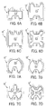
- FIGs.6A to 6D and FIGs.7A to 7D are plan views of micro openings respectively showing various actual examples according to the shape of the micro opening in the second embodiment.
- FIGs.8A to 8C are property graphs showing a secondary distribution of an optical strength of an optical near-field near the micro opening, which is obtained from a simulation.
- an optical near-field generating element 10' in this embodiment is provided with: the light guiding member 11 for guiding the light L1 outputted from the light source; and a light shielding member 12', which is placed on an optical path of the light L1 in the light guiding member 11, for defining a micro opening 20' having the diameter equal to or shorter than the wavelength of the light L1.
- the light guiding member 11 is composed of the optical fiber and the lens which are made of the light transmissive material, for example, such as glass, quartz, plastic and the like.
- the light shielding member 12' is made of the light shielding material in which the light transmittance is, for example, about 50 % or less. Actually, it is made of the light shielding material, for example, such as metallic film, alloy film, metallic silicide, organic film and the like.
- the light shielding member 12' is formed so as to cover the outer surface of the light guiding member 11 (the lower surface of the light guiding member 11 in FIG. 5 ) by deposition, coating and the like.
- the film thickness is, for example, from several nm to several hundred nm. However, the material and the film thickness are not especially limited as long as the micro opening 20' can be made.
- the light shielding member 12' is provided with a main portion for defining the basic shape of the micro opening 20' and a protrusion portion protruding from the main portion toward the center of the micro opening 20'.
- the diameter of the micro opening 20' defined by the main portion (namely, the portion except the protrusion portion) of the light shielding member 12' is set to be equal to or less than the wavelength of the light L1.
- the substantially spherical optical near-field L2 having the radius close to the diameter is generated within the air 50, on the output side (a lower side in FIG.5) of this micro opening 20'.
- the light shielding member 12' has a main portion for defining the micro opening 20', which is square as a basic shape, and a protrusion portion 31 protruding from the main portion toward the center of the micro opening 20', respectively, as shown in FIGs.6A to 6D. That is, FIG.6A is an actual example in which the light shielding member 12' has one protrusion portion 31. FIG.6B is an actual example in which the light shielding member 12' has two protrusion portions 31. FIG.6C is an actual example in which the light shielding member 12' has three protrusion portions 31. And, FIG.6D is an actual example in which the light shielding member 12' has four protrusion portions 31.
- the light shielding member 12' shown in FIG.5 has a main portion for defining the micro opening 20', which is circular as a basic shape, and a protrusion portion 31 protruding from the main portion toward the center of the micro opening 20', respectively, as shown in FIGs.7A to 7D. That is, FIG.7A is an actual example in which the light shielding member 12' has one protrusion portion 31. FIG.7B is an actual example in which the light shielding member 12' has two protrusion portions 31. FIG.7C is an actual example in which the light shielding member 12' has three protrusion portions 31. And, FIG.7D is an actual example in which the light shielding member 12' has four protrusion portions 31.
- the optical near-field generating element 10' having the above-mentioned configuration, when the light L1 is emitted from the light source, it is guided through the light guiding member 11.
- the micro opening 20' made on the light shielding member 12' causes the optical near-field L2 to be generated near the micro opening 20' on the side opposite to the input side of the light.
- the optical near-field L2 is in contact with the air 50, it stays near the micro opening 20, and it has no physical influence on the external field.
- the surface 60 of the object that can suck up the light from the optical near-field L2 approaches to a portion within several ten nm to several hundred mm, with respect to the surface of the light shielding member 12', namely, if it approaches to the existence region of the surface wave of the optical near-field L2, the light is emitted from the optical near-field L2 to the surface 60.
- the micro region to the degree of the existence of the optical near-field L2 can be used as a unit to emit the light.
- the record density in the optical memory can be made higher exceeding the diffractive limit, and the resolution in the fiber probe can be made higher exceeding the diffractive limit.
- the improvement of the usage efficiency of the light or the improvement of the light transmittance resulting from the special configuration that the protrusion portion 31 is used as shown in FIGs.6A to 7D is considered by a simulation.
- the calculation using the finite difference time domain method is carried out similarly to the above-mentioned case of the first embodiment.
- this simulation calculation is performed on three kinds of: (1) a case that the shape of the micro opening 20' is a square having sides of 120 nm as shown on the left side of FIG.8A; (2) a case that its basic shape is a square having sides of 120 nm and two protrusion portions are protruding by 20 nm in the upper and lower directions at the center as shown on the left side f FIG.8B; and (3) a case that its basic shape is a square having sides of 120 nm and two protrusion portions are protruding by 40 nm in the upper and lower directions at the center as shown in FIG.8C.
- FIGs.8A to 8C show the optical strengths of the optical near-fields in respective points (x, y) including the micro opening, which are obtained as the results of those simulation calculations, respectively.
- FIGs.8A to 8C show the optical strengths of the optical near-fields in the respective points (x, y) within the planes including the micro opening, respectively, on the z-axis.
- the scales indicative of the respective coordinates of x, y and z are relative. However, the scale settings based on the same unit are performed on the z-axis between FIGs.8A to 8C.
- the existence of the protrusion portion enables the existence region of the optical near-field to be smaller, and also enables the optical strength of the optical near-field to be higher.
- the greater the degree of the protrusion the smaller the existence region of the optical near-field, and the higher the optical strength of the optical near-field.
- the existence region of the optical near-field L2 can be made smaller and the optical strength can be made higher by selecting the shape of the micro opening 20' depending on a wavelength of light and the like which are determined depending on a concrete usage or actual adaptation of the optical near-field generating element 10'.
- the shape of the micro opening 20' and the like may be determined on the basis of the simulations as mentioned above, or may be done experimentally and experientially.
- the existence region of the optical near-field L2 can be made smaller, and at the same time, the usage efficiency of the light can be made higher, by forming the protrusion portion 31 on the micro opening 20' (refer to FIGs.6A to 7D), as compared with the conventional technique in which the shape of the micro opening is simple square, circular or the like.
- the basic shape of the micro opening 20' is not limited to the square or the circle as shown in FIGs.6A to 7D. It may be a polygon, such as a triangle, a pentagon, a hexagon, an octagon or the like, or an ellipse. Even in any case, the above-mentioned effects of making the existence region of the optical near-field smaller and further making its optical strength higher can be obtained more or less by protruding one or a plurality of protrusion portions from a side or a vertex of the basic shape.
- a plurality of such protrusion portions may be formed at positions point-symmetrical with the center of the micro opening 20'. Accordingly, it is possible to generate the optical near-field L2 point-symmetrical with the center of the micro opening 20' near the micro opening 20'.
- the light guiding member 11 made of glass and the like is placed on the light source side of the light shielding member 12' (the upper side of FIG.5).
- air can be used as the light guiding member as long as the optical near-field L2.is generated in the micro opening 20'.
- the optical near-field generating element in the third embodiment is designed such that the shape of the micro opening 20 in the configuration of the first embodiment shown in FIG.1 is replaced with the micro opening 20' whose shape is modified by using the protrusion portion 31, such as the second embodiment shown in FIGs.6A to 7D.
- the other configurations of the optical near-field generating element in the third embodiment are similar to those of the first embodiment.
- the protrusion portion formed on the light shielding member for defining the micro opening enables the existence region of the optical near-field to be made smaller, and also enables the optical strength to be made higher.
- the dielectric film adhered on the micro opening enables the optical strength to be made much higher.
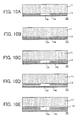
- FIGs.9A to 9D and FIGs.10A to 10E are enlarged sectional views respectively showing the portions near the optical near-field generating element, similarly to FIG.1.
- FIGs.9A to 9D show the variations in the first or third embodiment in which the dielectric film is formed on the micro opening, respectively.
- the film thickness of the dielectric film and the region or the position on which the dielectric film is formed are modified from those of the first or third embodiment.
- a dielectric film 13a is formed only within the micro opening, and the film thickness thereof is equal to that of the light shielding member 12.
- a dielectric film 13b is formed only within the micro opening, and the film thickness thereof is thinner than that of the light shielding member 12.
- a dielectric film 13c is formed within the micro opening and on the optical input side of the light shielding member 12.
- a dielectric film 13e is formed within the micro opening and on both the optical input side and the optical output side of the light shielding member 12.
- the dielectric film is adhered on the micro opening.
- the optical near-field can be made stronger.
- FIGs.10A to 10E show the variations of the first or third embodiments in which the dielectric film is formed on the micro opening, respectively.
- the variations of FIGs.10A to 10C are modified from the variations of FIGs.9A to 9C so that a metallic film is formed on the optical output side in the dielectric film.
- the variation of FIG.10D is modified from the first embodiment so that the metallic film is formed on the optical output side in the dielectric film.
- the variation of FIG.10E is modified from the variation of FIG.9D so that the metallic film is formed on the optical output side in the dielectric film.
- the dielectric film 13a is formed only within the micro opening, and the film thickness thereof is equal to that of the light shielding member 12, and a metallic film 14a is further formed on the optical output side thereof.
- the dielectric film 13b is formed only within the micro opening, and the film thickness thereof is thinner than that of the light shielding member 12, and a metallic film 14b is further formed on the optical output side thereof.
- the dielectric film 13c is formed within the micro opening and on the optical input side of the light shielding member 12, and a metallic film 14c is further formed on the optical output side thereof.
- the dielectric film 13d is formed within the micro opening and on the optical output side of the light shielding member 12, and a metallic film 14d is further formed on the optical output side thereof.
- the dielectric film 13e is formed within the micro opening and on both the optical input side and the optical output side of the light shielding member 12, and a metallic film 14e is further formed on the optical output side thereof.
- the dielectric film is adhered on the micro opening, and the metallic film is further formed.
- the optical near-field can be made stronger.
- the metallic film is formed on the optical output side of the dielectric film.
- such metallic film may be formed on the optical input side of the dielectric film in the first or third embodiment. Moreover, it may be formed on both the optical input side and the optical output side of the dielectric film.
- the various variations can be made to the first or third embodiment.
- the metallic films as shown in FIGs.10A to 10E may be formed on the optical output side or the optical input side.
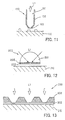
- FIG.11 is an enlarged sectional view showing a portion in which an optical near-field of the fiber probe is generated.
- a fiber probe 100 for an optical microscope has an optical fiber 101 serving as the light guiding member.
- the optical fiber 101 is coated with a metallic film 102 constituting the example of the light shielding member.
- a dielectric film 103 similar to that of the first embodiment is adhered on the micro opening made on the metallic film 102 at a tip of the optical fiber 101.
- the conventional fine machining technique enables the tip of the optical fiber 101 to be fine at about 20 to 30 nm. If the metallic film 102 is covered by coating or deposition, the configuration having the micro opening for the generation of the optical near-field can be relatively easily formed at the tip of the optical fiber 101. Then, the dielectric film 103 having a predetermined film thickness can be adhered on the tip.
- a mark or an image at a high resolution exceeding the diffraction limit can be produced on the surface of the target object 110 by the optical near-field which depends on the incident light L1 and has the small existence region.
- the mark or the image can be produced in a relatively short time by the optical near-field which depends on the incident light L1 and has the high optical strength.
- the protrusion portion (refer to FIGs.6A to 7D) may be formed on the metallic film 102 at the location for defining the micro opening, instead of or in addition to the formation of the dielectric film 103, similarly to the second or third embodiment.
- the fiber probe 100 in the fourth embodiment may be established as a built-in light source type of a fiber probe containing a light source.
- FIG.12 is an enlarged sectional view showing a portion in which an optical near-field of the optical head is generated.
- an optical head 200 for an optical memory which records data on an optically recording medium, such as an optical disc or the like, at a high density and reads out the data from the optical disc or the like, includes a solid immersion lens 201 as the light guiding member.
- a mask 202 constituting an example of the light shielding member is placed on a flat surface of the solid immersion lens 201.
- a dielectric film 203 similar to that of the first embodiment is adhered on the micro opening made on the mask 202 on the center of the flat surface of the solid immersion lens 201.
- the optical recording at a high density exceeding the diffraction limit can be attained by the optical near-field which depends on the incident light L1 and has the small existence region.
- the recording or the reproduction at a writing speed or a reading out speed which can be used on practical usage can be attained through the optical near-field that depends on the incident light L1 and has the high optical strength.
- the protrusion portion (refer to FIGs.6A to 7D) may be formed on the mask 202 at the location for defining the micro opening, instead of or in addition to the formation of the dielectric film 203, similarly to the second or third embodiment.
- optical head 200 in the fifth embodiment may be established as a built-in light source type of an optical head containing a light source.
- FIG.13 is an enlarged sectional view showing a portion in which an optical near-field of the probe array head is generated.
- a probe array head 300 for recording data on an optically recording medium, such as an optical disc or the like, at a high density and reading out the data from the optical disc or the like includes light shielding member(s) 302 for defining a plurality of arrayed micro openings.
- a dielectric film 303 similar to that of the first embodiment is adhered on those micro openings.
- the optical recording at the high density exceeding the diffraction limit can be attained by the optical near-field which depends on the incident light L1 and has the small existence region.
- the recording or the reproduction at the writing speed or the reading out speed which can be used on practical usage can be attained through the optical near-field that depends on the incident light L1 and has the high optical strength.
- the protrusion portion (refer to FIGs.6A to 7D) may be formed on the probe array head 300 at the location for defining the micro opening, instead of or in addition to the formation of the dielectric film 303, similarly to the second or third embodiment.
- the probe array head 300 in the sixth embodiment may be established as a built-in light source type of a probe array head containing a light source.
- optical apparatuses according to the fourth to sixth embodiments it can be applied to, for example, an optically fine machining apparatus, such as an exposing apparatus instead of a laser machining apparatus and the like, and various optical apparatuses, such as a device for an optical switch or an optical device for an optical communication system of an optical modulator, a light source and the like.
- an optically fine machining apparatus such as an exposing apparatus instead of a laser machining apparatus and the like
- various optical apparatuses such as a device for an optical switch or an optical device for an optical communication system of an optical modulator, a light source and the like.
- a first further preferred embodiment of the present invention is an optical near-field generating element, characterized in that said optical near-field generating element comprises: a light shielding member, which is placed on an optical path of light emitted from a light source, for defining a micro opening having a diameter equal to or shorter than a wavelength of the light; and a dielectric film placed in close contact with the micro opening.
- said micro opening has the diameter equal to or shorter than 1/2 of the wavelength of the light.
- a refractive index of said dielectric film is greater than that of an incident side of the optical path.
- said dielectric film comprises a single layer.
- said dielectric film comprises a plurality of layers.
- said optical near-field generating element comprises a metallic film having a light transmission characteristic and placed in close contact with the micro opening, instead of or in addition to said dielectric film.
- said light shielding member has a main portion for defining a basic shape of the micro opening and a protrusion portion protruding from the main portion toward the center of the micro opening.
- a third further preferred embodiment of the present invention is an optical near-field generating element, characterized in that said optical near-field generating element comprises a light shielding member, which is placed on an optical path of light emitted from a light source, for defining a micro opening having a diameter equal to or shorter than a wavelength of the light, and said shielding member comprises: a main portion for defining a basic shape of the micro opening; and a protrusion portion protruding from the main portion toward the center of the micro opening.
- said basic shape of the micro opening is a polygon, a circle or an oval.
- a plurality of protrusion portions are placed at positions point-symmetrical with the center of the micro opening.
- Said optical near-field generating element may further comprise a light guiding member for guiding the light emitted from the light source, and said light shielding member may be placed at a tip of said light guiding member in the forward direction of the light.
- Said light guiding member may be an optical fiber.
- Said optical fiber may be covered with a metallic film and said light shielding member may comprise the metallic film.
- Said light guiding member may also comprise a solid immersion lens.
- said optical near-field generating element may include the light source.
- a fourth further preferred embodiment of the present invention is an optical apparatus, characterized in that said optical apparatus comprises an optical near-field generating element, and said optical near-field generating element comprises: a light shielding member, which is placed on an optical path of light emitted from a light source, for defining a micro opening having a diameter equal to or shorter than a wavelength of the light; and a dielectric film placed in close contact with the micro opening.
- a fifth further preferred embodiment of the present invention is an optical apparatus, characterized in that said optical apparatus comprises an optical near-field generating element, said optical near-field generating element comprises a light shielding member, which is placed on an optical path of light emitted from a light source, for defining a micro opening having a diameter equal to or shorter than a wavelength of the light, and said shielding member comprising: a main portion for defining a basic shape of the micro opening; and a protrusion portion protruding from the main portion toward the center of the micro opening.
- said optical apparatus comprises a plurality of said optical near-field generating elements with them arrayed.
Landscapes
- Physics & Mathematics (AREA)
- Optics & Photonics (AREA)
- Chemical & Material Sciences (AREA)
- Engineering & Computer Science (AREA)
- Nanotechnology (AREA)
- Nuclear Medicine, Radiotherapy & Molecular Imaging (AREA)
- Crystallography & Structural Chemistry (AREA)
- Health & Medical Sciences (AREA)
- General Health & Medical Sciences (AREA)
- General Physics & Mathematics (AREA)
- Radiology & Medical Imaging (AREA)
- Biophysics (AREA)
- Analytical Chemistry (AREA)
- Life Sciences & Earth Sciences (AREA)
- Optical Head (AREA)
- Optical Couplings Of Light Guides (AREA)
Applications Claiming Priority (3)
| Application Number | Priority Date | Filing Date | Title |
|---|---|---|---|
| JP2001236110A JP2003042930A (ja) | 2001-08-03 | 2001-08-03 | 近接場光発生素子及びこれを具備してなる光学装置 |
| JP2001236110 | 2001-08-03 | ||
| EP02017410A EP1282121A3 (de) | 2001-08-03 | 2002-08-02 | Element zur Erzeugung eines optischen Nahfeldes und ein dieses Element beinhaltendes optisches Gerät |
Related Parent Applications (1)
| Application Number | Title | Priority Date | Filing Date |
|---|---|---|---|
| EP02017410A Division EP1282121A3 (de) | 2001-08-03 | 2002-08-02 | Element zur Erzeugung eines optischen Nahfeldes und ein dieses Element beinhaltendes optisches Gerät |
Publications (1)
| Publication Number | Publication Date |
|---|---|
| EP1501088A1 true EP1501088A1 (de) | 2005-01-26 |
Family
ID=19067445
Family Applications (2)
| Application Number | Title | Priority Date | Filing Date |
|---|---|---|---|
| EP04024969A Withdrawn EP1501088A1 (de) | 2001-08-03 | 2002-08-02 | Element zur Erzeugung eines optischen Nahfeldes und ein dieses Element beinhaltendes optisches Gerät |
| EP02017410A Withdrawn EP1282121A3 (de) | 2001-08-03 | 2002-08-02 | Element zur Erzeugung eines optischen Nahfeldes und ein dieses Element beinhaltendes optisches Gerät |
Family Applications After (1)
| Application Number | Title | Priority Date | Filing Date |
|---|---|---|---|
| EP02017410A Withdrawn EP1282121A3 (de) | 2001-08-03 | 2002-08-02 | Element zur Erzeugung eines optischen Nahfeldes und ein dieses Element beinhaltendes optisches Gerät |
Country Status (3)
| Country | Link |
|---|---|
| US (2) | US6839191B2 (de) |
| EP (2) | EP1501088A1 (de) |
| JP (1) | JP2003042930A (de) |
Families Citing this family (17)
| Publication number | Priority date | Publication date | Assignee | Title |
|---|---|---|---|---|
| JP2004356134A (ja) * | 2003-05-27 | 2004-12-16 | Canon Inc | 微小構造の加工方法、該加工法を用いて作製した微小素子の作製方法、微小素子 |
| JP4350446B2 (ja) * | 2003-07-11 | 2009-10-21 | キヤノン株式会社 | 電場の発生方法、電場の発生装置 |
| US7149395B1 (en) * | 2005-08-09 | 2006-12-12 | Instrument Technology Research Center | Light-enhancing component and fabrication method thereof |
| JP2007333497A (ja) * | 2006-06-14 | 2007-12-27 | Hitachi High-Technologies Corp | 蛍光検出デバイスおよび装置 |
| US8737178B2 (en) * | 2006-09-05 | 2014-05-27 | Seagate Technology Llc | Alignment feature for near-field transducers |
| US7759630B2 (en) * | 2006-12-26 | 2010-07-20 | Hitachi Global Storage Technologies Netherlands B.V. | Method and apparatus for the generation and control of multiple near-field light sources at subwavelength resolution |
| US8243557B2 (en) * | 2006-12-26 | 2012-08-14 | Hitachi Global Storage Technologies Netherlands B.V. | Optimized ridge apertures for thermally assisted magnetic recording |
| US8092704B2 (en) * | 2008-12-30 | 2012-01-10 | Hitachi Global Storage Technologies Netherlands B.V. | System, method and apparatus for fabricating a c-aperture or E-antenna plasmonic near field source for thermal assisted recording applications |
| US8472286B2 (en) | 2008-12-31 | 2013-06-25 | HGST Netherlands B.V. | Near field transducer having main body and wings extending therefrom and only electrically coupled thereby |
| US7880996B2 (en) * | 2008-12-31 | 2011-02-01 | Hitachi Global Storage Technologies Netherlands B.V. | Ridge wave-guide for thermal assisted magnetic recording |
| US8169881B2 (en) * | 2008-12-31 | 2012-05-01 | Hitachi Global Storage Technologies Netherlands B.V. | Thermally assisted recording head having recessed waveguide with near field transducer and methods of making same |
| EP2810298A1 (de) | 2012-02-03 | 2014-12-10 | Seagate Technology LLC | Verfahren zur herstellung von schichten |
| US9280989B2 (en) | 2013-06-21 | 2016-03-08 | Seagate Technology Llc | Magnetic devices including near field transducer |
| US8830800B1 (en) * | 2013-06-21 | 2014-09-09 | Seagate Technology Llc | Magnetic devices including film structures |
| US20160275972A1 (en) | 2015-03-22 | 2016-09-22 | Seagate Technology Llc | Devices including metal layer |
| WO2016191666A1 (en) | 2015-05-28 | 2016-12-01 | Seagate Technology Llc | Near field transducers (nfts) including barrier layer and methods of forming |
| US9672848B2 (en) | 2015-05-28 | 2017-06-06 | Seagate Technology Llc | Multipiece near field transducers (NFTS) |
Citations (3)
| Publication number | Priority date | Publication date | Assignee | Title |
|---|---|---|---|---|
| US5689480A (en) * | 1996-08-13 | 1997-11-18 | The Board Of Trustees Of The Leland Stanford Junior University | Magneto-optic recording system employing near field optics |
| US5696372A (en) * | 1996-07-31 | 1997-12-09 | Yale University | High efficiency near-field electromagnetic probe having a bowtie antenna structure |
| EP1148370A2 (de) * | 2000-03-13 | 2001-10-24 | Hitachi, Ltd. | Optische Nahfeldsonde, optisches Nahfeldmikroskop und optisches Aufzeichnungs-/Wiedergabegerät mit optischer Nahfeldsonde |
Family Cites Families (13)
| Publication number | Priority date | Publication date | Assignee | Title |
|---|---|---|---|---|
| JPH10293134A (ja) * | 1997-02-19 | 1998-11-04 | Canon Inc | 光検出または照射用のプローブ、及び該プローブを備えた近視野光学顕微鏡・記録再生装置・露光装置、並びに該プローブの製造方法 |
| US5973316A (en) * | 1997-07-08 | 1999-10-26 | Nec Research Institute, Inc. | Sub-wavelength aperture arrays with enhanced light transmission |
| JP3697034B2 (ja) * | 1997-08-26 | 2005-09-21 | キヤノン株式会社 | 微小開口を有する突起の製造方法、及びそれらによるプローブまたはマルチプローブ |
| JPH11265520A (ja) * | 1998-03-17 | 1999-09-28 | Hitachi Ltd | 近接場光ヘッド、近接場光ヘッドの加工方法および光記録再生装置 |
| US6040936A (en) * | 1998-10-08 | 2000-03-21 | Nec Research Institute, Inc. | Optical transmission control apparatus utilizing metal films perforated with subwavelength-diameter holes |
| US6541755B1 (en) * | 1998-11-25 | 2003-04-01 | Ricoh Company, Ltd. | Near field optical probe and manufacturing method thereof |
| JP2000206315A (ja) * | 1999-01-12 | 2000-07-28 | Hitachi Ltd | 微細光記録装置 |
| JP3901867B2 (ja) * | 1999-02-08 | 2007-04-04 | 富士フイルム株式会社 | 近接場光記録再生装置 |
| JP2001013056A (ja) * | 1999-07-02 | 2001-01-19 | Minolta Co Ltd | 微小開口形成方法 |
| US6285020B1 (en) * | 1999-11-05 | 2001-09-04 | Nec Research Institute, Inc. | Enhanced optical transmission apparatus with improved inter-surface coupling |
| US6574257B1 (en) * | 2000-02-01 | 2003-06-03 | Siros Technologies, Inc. | Near-field laser and detector apparatus and method |
| JP3793430B2 (ja) * | 2001-07-18 | 2006-07-05 | 株式会社日立製作所 | 近接場光を用いた光学装置 |
| JP3932944B2 (ja) * | 2002-03-27 | 2007-06-20 | 日本電気株式会社 | 光学素子およびそれを用いた光ヘッド |
-
2001
- 2001-08-03 JP JP2001236110A patent/JP2003042930A/ja active Pending
-
2002
- 2002-08-02 EP EP04024969A patent/EP1501088A1/de not_active Withdrawn
- 2002-08-02 EP EP02017410A patent/EP1282121A3/de not_active Withdrawn
- 2002-08-02 US US10/209,975 patent/US6839191B2/en not_active Expired - Fee Related
-
2004
- 2004-08-13 US US10/917,366 patent/US6970307B2/en not_active Expired - Fee Related
Patent Citations (3)
| Publication number | Priority date | Publication date | Assignee | Title |
|---|---|---|---|---|
| US5696372A (en) * | 1996-07-31 | 1997-12-09 | Yale University | High efficiency near-field electromagnetic probe having a bowtie antenna structure |
| US5689480A (en) * | 1996-08-13 | 1997-11-18 | The Board Of Trustees Of The Leland Stanford Junior University | Magneto-optic recording system employing near field optics |
| EP1148370A2 (de) * | 2000-03-13 | 2001-10-24 | Hitachi, Ltd. | Optische Nahfeldsonde, optisches Nahfeldmikroskop und optisches Aufzeichnungs-/Wiedergabegerät mit optischer Nahfeldsonde |
Non-Patent Citations (1)
| Title |
|---|
| YOUNG-JOO KIM ET AL: "Parallel recording array head of nano-aperture flat-tip probes for high-density near-field optical data storage", 10TH INTERNATIONAL SYMPOSIUM ON OPTICAL MEMORY 2000 (ISOM 2000), HOKKAIDO, JAPAN, 5-8 SEPT. 2000, vol. 40, no. 3B, 5 September 2000 (2000-09-05), Japanese Journal of Applied Physics, Part 1 (Regular Papers, Short Notes & Review Papers), March 2001, Japan Soc. Appl. Phys, Japan, pages 1783 - 1789, XP002222850, ISSN: 0021-4922 * |
Also Published As
| Publication number | Publication date |
|---|---|
| JP2003042930A (ja) | 2003-02-13 |
| US6970307B2 (en) | 2005-11-29 |
| EP1282121A3 (de) | 2003-05-21 |
| US20030128945A1 (en) | 2003-07-10 |
| US20050008296A1 (en) | 2005-01-13 |
| US6839191B2 (en) | 2005-01-04 |
| EP1282121A2 (de) | 2003-02-05 |
Similar Documents
| Publication | Publication Date | Title |
|---|---|---|
| US6970307B2 (en) | Optical near-field generating element and optical apparatus including the same | |
| JP4130656B2 (ja) | 光学ヘッド及び情報記憶装置 | |
| JP4094229B2 (ja) | 近視野光ヘッドおよびその製造方法 | |
| US7171080B2 (en) | Coupling grating for focusing light within a waveguide for heat assisted magnetic recording | |
| US7057151B2 (en) | Optical transmission apparatus with directionality and divergence control | |
| US20150043048A1 (en) | Super-oscillatory lens device | |
| EP0924524A1 (de) | Faseroptische sonde und verfahren zu deren herstellung | |
| EP1385175A1 (de) | Design einer Sondenspitze für ein optisches Nahfeldmikroskop | |
| KR20010091859A (ko) | 근접장 광프로브 및 이를 이용한 근접장 광학 현미경 및광기록/재생 장치 | |
| CN113687465B (zh) | 基于全介质超表面的表面等离激元近场聚焦透镜 | |
| EP1139121B1 (de) | Verfahren zur Herstellung lichterzeugender Nahfeld-Elemente | |
| KR100525241B1 (ko) | 전위차를 이용한 광섬유 탐침 및 그를 이용한 광기록 장치 | |
| JP4681162B2 (ja) | 近視野光発生素子の作製方法 | |
| JP4260645B2 (ja) | 近視野光ヘッドの製造方法 | |
| KR100584987B1 (ko) | 표면 플라즈몬파를 이용한 피라미드 형상의 근접장 탐침 | |
| JP3592546B2 (ja) | 高出力光プローブおよび光システム | |
| JPH04291310A (ja) | 近距離場走査光学顕微鏡及びその用途 | |
| Hirota et al. | Design of a Near-Field Probe for Optical Recording Using a 3-Dimensional Finite Difference Time Domain Method | |
| JP4567071B2 (ja) | 光学ヘッド及び情報記憶装置 | |
| JP3662134B2 (ja) | 平面型プローブ及びその形成方法 | |
| JP2002532733A (ja) | 準波長域の開口が形成されてなりレンズを有する光ファイバ及び独特のマイクロピペット | |
| JP3892264B2 (ja) | 近視野光発生素子の作製方法 | |
| JP3157754B2 (ja) | 平面プローブ及びその製造方法 | |
| JP2002008235A (ja) | プラズモンを用いた記録再生装置およびその作製法 | |
| Wang et al. | Super-resolution near-field imaging on microfluidic structure |
Legal Events
| Date | Code | Title | Description |
|---|---|---|---|
| PUAI | Public reference made under article 153(3) epc to a published international application that has entered the european phase |
Free format text: ORIGINAL CODE: 0009012 |
|
| AC | Divisional application: reference to earlier application |
Ref document number: 1282121 Country of ref document: EP Kind code of ref document: P |
|
| AK | Designated contracting states |
Kind code of ref document: A1 Designated state(s): DE FR GB |
|
| RIN1 | Information on inventor provided before grant (corrected) |
Inventor name: YAMAKAWA, YUZO,C/O PIONEER CORPORATION Inventor name: SUGIURA, SATOSHI,C/O PIONEER CORPORATION |
|
| 17P | Request for examination filed |
Effective date: 20050407 |
|
| AKX | Designation fees paid |
Designated state(s): DE FR GB |
|
| 17Q | First examination report despatched |
Effective date: 20071219 |
|
| STAA | Information on the status of an ep patent application or granted ep patent |
Free format text: STATUS: THE APPLICATION IS DEEMED TO BE WITHDRAWN |
|
| 18D | Application deemed to be withdrawn |
Effective date: 20090703 |