US8092704B2 - System, method and apparatus for fabricating a c-aperture or E-antenna plasmonic near field source for thermal assisted recording applications - Google Patents
System, method and apparatus for fabricating a c-aperture or E-antenna plasmonic near field source for thermal assisted recording applications Download PDFInfo
- Publication number
- US8092704B2 US8092704B2 US12/345,715 US34571508A US8092704B2 US 8092704 B2 US8092704 B2 US 8092704B2 US 34571508 A US34571508 A US 34571508A US 8092704 B2 US8092704 B2 US 8092704B2
- Authority
- US
- United States
- Prior art keywords
- aperture
- insulator layer
- layer
- hard mask
- gap
- Prior art date
- Legal status (The legal status is an assumption and is not a legal conclusion. Google has not performed a legal analysis and makes no representation as to the accuracy of the status listed.)
- Expired - Fee Related, expires
Links
Images


Classifications
-
- G—PHYSICS
- G11—INFORMATION STORAGE
- G11B—INFORMATION STORAGE BASED ON RELATIVE MOVEMENT BETWEEN RECORD CARRIER AND TRANSDUCER
- G11B5/00—Recording by magnetisation or demagnetisation of a record carrier; Reproducing by magnetic means; Record carriers therefor
- G11B5/127—Structure or manufacture of heads, e.g. inductive
- G11B5/31—Structure or manufacture of heads, e.g. inductive using thin films
- G11B5/3109—Details
- G11B5/313—Disposition of layers
- G11B5/3133—Disposition of layers including layers not usually being a part of the electromagnetic transducer structure and providing additional features, e.g. for improving heat radiation, reduction of power dissipation, adaptations for measurement or indication of gap depth or other properties of the structure
- G11B5/314—Disposition of layers including layers not usually being a part of the electromagnetic transducer structure and providing additional features, e.g. for improving heat radiation, reduction of power dissipation, adaptations for measurement or indication of gap depth or other properties of the structure where the layers are extra layers normally not provided in the transducing structure, e.g. optical layers
-
- G—PHYSICS
- G11—INFORMATION STORAGE
- G11B—INFORMATION STORAGE BASED ON RELATIVE MOVEMENT BETWEEN RECORD CARRIER AND TRANSDUCER
- G11B5/00—Recording by magnetisation or demagnetisation of a record carrier; Reproducing by magnetic means; Record carriers therefor
- G11B5/127—Structure or manufacture of heads, e.g. inductive
- G11B5/31—Structure or manufacture of heads, e.g. inductive using thin films
- G11B5/3163—Fabrication methods or processes specially adapted for a particular head structure, e.g. using base layers for electroplating, using functional layers for masking, using energy or particle beams for shaping the structure or modifying the properties of the basic layers
-
- G—PHYSICS
- G11—INFORMATION STORAGE
- G11B—INFORMATION STORAGE BASED ON RELATIVE MOVEMENT BETWEEN RECORD CARRIER AND TRANSDUCER
- G11B5/00—Recording by magnetisation or demagnetisation of a record carrier; Reproducing by magnetic means; Record carriers therefor
- G11B5/48—Disposition or mounting of heads or head supports relative to record carriers ; arrangements of heads, e.g. for scanning the record carrier to increase the relative speed
- G11B5/58—Disposition or mounting of heads or head supports relative to record carriers ; arrangements of heads, e.g. for scanning the record carrier to increase the relative speed with provision for moving the head for the purpose of maintaining alignment of the head relative to the record carrier during transducing operation, e.g. to compensate for surface irregularities of the latter or for track following
- G11B5/60—Fluid-dynamic spacing of heads from record-carriers
- G11B5/6005—Specially adapted for spacing from a rotating disc using a fluid cushion
- G11B5/6088—Optical waveguide in or on flying head
-
- G—PHYSICS
- G11—INFORMATION STORAGE
- G11B—INFORMATION STORAGE BASED ON RELATIVE MOVEMENT BETWEEN RECORD CARRIER AND TRANSDUCER
- G11B5/00—Recording by magnetisation or demagnetisation of a record carrier; Reproducing by magnetic means; Record carriers therefor
- G11B2005/0002—Special dispositions or recording techniques
- G11B2005/0005—Arrangements, methods or circuits
- G11B2005/0021—Thermally assisted recording using an auxiliary energy source for heating the recording layer locally to assist the magnetization reversal
Definitions
- the present invention relates in general to thermal assisted recording (TAR) applications and, in particular, to an improved system, method and apparatus for fabricating a c-aperture or IS-antenna plasmonic near field source for thermal assisted recording applications in hard disk drives.
- TAR thermal assisted recording
- the magnetic material (or media) for the recording layer on the disk is chosen to have sufficient coercivity such that the magnetized data bits are written precisely and retain their magnetization state until written over by new data bits.
- the areal data density the number of bits that can be recorded on a unit surface area of the disk
- the magnetic grains that make up the data bits can be so small that they can be demagnetized simply from thermal instability or agitation within the magnetized bit (the so-called “superparamagnetic” effect).
- K u magneto-crystalline anisotropy
- H 0 is the field required to reverse the magnetization direction, which for most magnetic materials is somewhat greater than the coercivity or coercive field measured on much longer time-scales.
- H 0 cannot exceed the write field capability of the recording head, which currently is limited to about 15 kOe for perpendicular recording.
- TAR thermally-assisted recording
- the magnetic material is heated locally to near or above its Curie temperature during writing to lower the coercivity enough for writing to occur, but where the coercivity/anisotropy is high enough for thermal stability of the recorded bits at the ambient temperature of the disk drive (i.e., the normal operating or “room” temperature).
- TAR approaches have been proposed, primarily for the more conventional longitudinal or horizontal recording, wherein the magnetizations of the recorded bits are oriented generally in-the-plane of the recording layer.
- TAR is also applicable for perpendicular recording, wherein the magnetizations of the recorded bits are oriented generally out-of-the-plane of the recording layer.
- TAR is also usable with patterned media.
- TAR it is important to avoid heating data tracks adjacent to the data track where data is to be written because the stray magnetic field from the write head can erase data previously recorded in the adjacent tracks. Also, even in the absence of a magnetic field, heating of adjacent data tracks accelerates the thermal decay over that at ambient temperature and thus data loss may occur.
- a proposed solution for this adjacent-track interference problem is the use of an optical channel with a small aperture that directs heat from a radiation source, such as a laser, to heat just the data track where data is to be written. This type of TAR disk drive is described in U.S. Pat. No. 5,583,727 and U.S. Pat. No. 6,982,844.
- each read/write head is located on an air-bearing slider that is maintained in close proximity to its associated disk surface as the disks rotate.
- the films making up the read and write heads are deposited on a wafer containing a large number, e.g., 40,000, of rectangular regions arranged in rows, with each region ultimately becoming an individual slider.
- the wafer is cut into rows and the rows cut into individual sliders.
- the sliders are then “lapped” in a plane perpendicular to the wafer surface, with this plane becoming the slider's air-bearing surface (ABS).
- TAR requires small focused light spots that are much smaller than the diffraction limit of the light source. Therefore, regular optical components are not viable for these types of applications.
- Nanoscale near field plasmonic sources are being considered for use in TAR for fabricating the required optical structures.
- One of the most promising optical structures is the c-aperture, which can be thought of as an E-antenna.
- the dielectric aperture in this structure looks like the letter “c”, while the metal surrounding that dielectric forms an antenna in the shape of a capital letter “E”.
- EA improved wafer-level process for forming optical channels and aperture structures on air-bearing sliders for use in TAR disk drives would be desirable.
- Embodiments of a system, method, and apparatus for fabricating a c-aperture or E-antenna plasmonic near field source for thermal assisted recording applications in hard disk drives are disclosed.
- the invention comprises a technique for building a c-aperture in a manner that is consistent with and appropriate for recording head applications.
- the technique employs e-beam lithography, partial reactive ion etching (RIE) and metal refill to build the c-apertures.
- RIE reactive ion etching
- FIG. 1 is a schematic sectional side view of one embodiment of a thermal assisted recording (TAR) head for a hard disk drive, and is constructed in accordance with the invention
- FIG. 2 is an enlarged schematic sectional air bearing surface (ABS) view of one embodiment of a c-aperture writer for the TAR head of FIG. 1 , rotated 90 degrees, and is constructed in accordance with the invention;
- ABS air bearing surface
- FIGS. 3-13 are schematic sectional and top views of various embodiments of a method of fabricating the c-aperture of FIG. 2 , and are constructed in accordance with the invention;
- FIG. 14 is a sectional view through one embodiment of a portion of an air-bearing slider and associated perpendicular magnetic recording disk for a TAR disk drive that uses an optical channel and aperture structure to direct heat to the recording layer of the disk in accordance with the invention
- FIG. 15 is an illustration of one embodiment of the radiation exit face of an aperture structure having a generally c-shaped aperture with a characteristic dimension “d,” and is constructed in accordance with the invention
- FIG. 16 is a perspective view of one embodiment of a portion of a wafer showing a plurality of generally rectangular regions in accordance with the invention.
- FIG. 17 is a perspective view of one embodiment of an aperture structure on a rectangular region of the wafer in accordance with the invention.
- FIGS. 1-17 embodiments of a system, method and apparatus for fabricating a c-aperture or E-antenna plasmonic near field source for thermal assisted recording applications in hard disk drives are disclosed.
- FIG. 14 is a sectional view through a portion of an air-bearing slider 110 and associated perpendicular magnetic recording disk for a TAR disk drive of the type that uses an optical channel for directing heat to the disk.
- the disk 140 includes a substrate 142 , an optional “soft” or relatively low-coercivity magnetically permeable underlayer (SUL) 144 , and a perpendicular magnetic recording layer (RL) 146 .
- the SUL 144 is not required for a TAR disk drive but if used is typically any alloy material suitable as the magnetically-permeable flux-return path, such as NiFe, FeAlSi, FeTaN, FeN, CoFeB and CoZrNb.
- the RL 146 may be any media with perpendicular magnetic anisotropy, such as a cobalt-chromium (CoCr) alloy granular layer grown on a special growth-enhancing sublayer, or a multilayer of alternating films of Co with films of platinum (Pt) or palladium (Pd).
- the RL 146 may also be an L1 0 ordered alloy such as FePt or FeNiPt.
- the disk 140 would also typically include a protective overcoat (not shown) over the RL 146 .
- the slider 110 has a trailing surface 111 and an air-bearing surface (ABS) surface 112 oriented generally perpendicular to trailing surface 111 .
- the slider 110 is typically formed of a composite material, such as a composite of alumina/titanium-carbide (Al 2 O 3 /TiC), and supports the read and write elements typically formed as a series of thin films and structures on its trailing surface 111 .
- the surface 111 is called the trailing surface because of the direction 123 of the disk 140 relative to slider 110 .
- the ABS 112 is the recording-layer-facing surface of the slider that faces the disk and is shown without the thin protective overcoat typically present in an actual slider.
- the recording-layer-facing surface or ABS shall mean the surface of the slider that is covered with a thin protective overcoat, the actual outer surface of the slider if there is no overcoat, or the outer surface of the overcoat.
- FIG. 14 is not drawn to scale because of the difficulty in showing the very small features.
- the slider 110 supports a conventional magnetoresistive read head 115 located between shields S 1 and S 2 , and a conventional perpendicular write head that includes a magnetic yoke 120 with a write pole 120 a , a flux return pole 120 b , and an electrically conductive coil 125 .
- the write pole 120 a is formed of conventional high-moment material, such as a FeCoNi alloy.
- the write coil 125 is shown as wrapped around yoke 120 with the electrical current directions being shown as into the paper by the coil cross-sections marked with an “X” and out of the paper by the coil cross-sections marked with a solid circle.
- the write pole 120 a When write-current pulses are directed through coil 125 , the write pole 120 a directs magnetic flux, represented by arrow 122 , to the RL 146 .
- the dashed line 130 with arrows show the flux return path through the SUL 144 back to the return pole 120 b .
- the coil may also be of the helical type.
- the slider 110 also includes a waveguide or optical channel 150 with an aperture structure 160 near the ABS 112 .
- the optical channel 150 with aperture structure 160 is depicted in FIG. 14 as extending through the yoke 120 and being located between the write pole 120 a and the return pole 120 b .
- the optical channel 150 with aperture structure 160 may be fabricated on the trailing surface 111 at other locations, such as between shield S 2 and return pole 120 b , or between the write pole 120 a and the outer face 131 of slider 110 .
- the optical channel 150 is formed of a core material 151 such as a high-index-of-refraction dielectric material that is transmissive to radiation at the wavelength of the laser radiation source.
- Typical radiation-transmissive materials include TiO 2 and Ta 2 O 5 .
- the radiation-transmissive material 151 is surrounded by cladding material 152 a , 152 b that has a lower refractive index than the optical channel material 151 and is transmissive to radiation at the wavelength of the laser radiation source.
- Typical cladding materials include SiO 2 and Al 2 O 3 .
- the optical channel 150 directs radiation to the aperture structure 160 .
- Aperture structure 160 includes the opening or aperture 161 that is filled with radiation-transmissive material and that is surrounded by metal layer 162 .
- the aperture 161 is filled with a low index of refraction material such as SiO 2 or Al 2 O 3
- the aperture structure 160 has a radiation entrance face 163 and a radiation exit face 164 that are generally parallel to one another and to the ABS.
- the aperture structure 160 directs radiation, as represented by wavy arrow 166 , to the RL 146 to heat the RL nearly to or above the Curie temperature of the material making up the RL.
- the RL 146 moves relative to the slider 110 in the direction shown by arrow 123 .
- heating from radiation through aperture structure 160 temporarily lowers the coercivity H c of the RL 146 so that the magnetic regions may be oriented by the write field from write pole 120 a .
- the magnetic regions become oriented by the write field if the write field H w is greater than H c .
- H w the write field
- H c the write field
- the transitions between recorded regions (such as previously recorded regions 127 , 128 and 129 ) represent written data “bits” that can be read by the read head 115 .
- the wavelength is approximately 780 nm.
- the laser diode may be located on the slider 110 .
- laser radiation may be delivered from a source off the slider through an optical fiber or waveguide.
- the aperture 161 at radiation exit face 164 acts as a near-field optical transducer.
- the aperture 161 is subwavelength-sized, i.e., the dimension of its smallest feature is less than the wavelength of the incident laser radiation and preferably less than one-half the wavelength of the laser radiation.
- FIG. 15 is a view of radiation exit face 164 with aperture 161 surrounded by metal 162 .
- the aperture 161 shown in FIG. 15 is a “C”-shaped aperture with a characteristic dimension “d.”
- the near-field spot size is determined by the characteristic dimension “d,” which is the width of the ridge of the aperture.
- the resonant wavelength depends on the characteristic dimension of the aperture as well as the electrical properties and thickness of the thin film surrounding the aperture. This is discussed by J. A. Matteo et. al., Applied Physics Letters , Volume 85(4), pp. 648-650 (2004) for a C-shaped aperture.
- the films making up the read and write heads are deposited on a wafer containing a large number, e.g., 40,000, of rectangular regions arranged in rows, with each region ultimately becoming an individual slider and the wafer surface of each region becoming the trailing surface of the individual slider, like trailing surface 111 of slider 110 .
- the wafer is cut into rows and the rows cut into individual sliders. The sliders are then “lapped” in a plane perpendicular to the wafer surface, with this plane becoming the slider ABS.
- the aperture structures, as well as the optical channels are fabricated at the wafer level.
- each slider contains not only the read and write heads, but the aperture structure and optical channel required for TAR, like the slider shown in FIG. 14 .
- FIG. 16 is a perspective view of a portion of a wafer 170 .
- the wafer 170 has a generally planar upper surface and a plurality of generally rectangular regions 180 arranged in generally parallel rows 190 , with each region 180 being shown bounded by dashed lines 191 , 192 .
- Each region 180 has an optical channel 150 and aperture structure 160 .
- the wafer 170 is cut into rows 190 along planes represented by dashed lines 191 , and the rows 190 then cut along planes represented by dashed lines 192 , to form the individual sliders.
- the sliders are lapped, either at the row level or the individual slider level, along planes parallel to planes represented by dashed lines 191 , to define the ABS.
- the wafer 170 has a thickness “t” which is the “length” of the individual sliders.
- FIG. 17 is a perspective view, not to scale, of an aperture structure 160 on a rectangular region 180 of wafer 170 .
- the aperture structure 160 includes the aperture 161 surrounded by metal 162 , which may be a pure metal, such as Au or Cu, or an alloy of two or more metals, like a AuCu alloy.
- the aperture structure 160 has parallel faces 163 , 164 that are generally parallel to the plane 191 along which the wafer will be cut into rows of rectangular regions.
- the aperture 161 has a generally C-shape defined by a ridge 165 of metal 162 that extends between faces 163 and 164 .
- FIG. 17 also shows one embodiment of dimensions for the aperture structure 160 , which are meant to be merely representative of typical dimensions and do not limit the scope of the invention.
- the aperture structure 160 has a width parallel to plane 191 and to the “length” of rectangular region 180 of about 400 to 800 nm and a thickness of about 200 to 400 nm in the direction perpendicular to the wafer surface.
- the ridge 165 has a width of about 30 nm and a thickness of about 30 nm, with the characteristic dimension “d” of the C-shaped aperture being the width of ridge 165 .
- the size of the ridge 165 and the characteristic dimension “d” essentially define the spot size of the radiation incident on the recording layer, and for the dimensions shown the areal bit density on the disk would be greater than about 1 Terabit/in 2 .
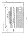
- FIG. 1 depicts an embodiment of a thermal assisted recording (TAR) head 21 for a hard disk drive.
- TAR head 21 comprises a main pole 23 , a core 25 and cladding 27 , 29 , 31 formed thereon and therebetween.
- the cladding 27 , 29 , 31 may comprise Al 2 O 3 having a thickness on the order of 1 to 2 ⁇ m.
- One embodiment of the core 25 has a thickness of about 300 nm and an aperture and lip thickness of about 525 nm.
- Another separate layer of cladding 33 e.g., SiO 2
- TAR head 21 may further comprise a stitch pole 35 having a thickness of about 1 ⁇ m, and an aperture 41 having an aperture and lip throat height of about 90 nm, in one embodiment.
- FIG. 2 is an enlarged schematic sectional ABS view of one embodiment of the aperture 41 .
- aperture 41 may comprise a c-aperture or E-antenna writer.
- aperture 41 comprises a substrate (e.g., formed from NiFe), a stitch pole 45 , and a base layer or magnetic lip 47 which may be formed from a core of CoFe or similar magnetic material.
- An insulation layer 49 is formed on the magnetic lip 47 , is encased in a conductive material 51 , and has cladding 27 .
- the insulation layer 49 is formed from SiO 2 , has a thickness of about 60 nm, and has a central rectangular notch 53 (e.g., 30 ⁇ 30 nm) formed therein opposite the magnetic lip 47 .
- the conductive material 51 may comprise Au and have a width of about 500 nm.
- the thickness of magnetic lip 47 is about 300 nm, and conductive material 51 has a thickness of about 120 nm.
- FIGS. 3-13 schematic sectional and top views of various embodiments of a method of fabricating the aperture 41 depicted in FIG. 2 are shown.
- the method fabricates a plasmonic near field source for thermal assisted recording applications in, for example, hard disk drives.
- the method initially comprises depositing an insulator 61 (which will ultimately be the insulation layer 49 ) on a “base layer” 63 (which will ultimately be the magnetic lip 47 ).
- an e-beam resist layer 65 is applied on the insulator 61 .
- FIGS. 5 and 6 depict sectional side and top views of e-beam lithography and liftoff on the e-beam resist layer to form a pair of parallel hard mask features 67 separated by a gap 69 .
- the insulator layer 61 is then reactive ion etched (RIE) to form a notch 53 in the insulation layer 49 below the gap 69 .
- the hard mask features 67 protect the insulator material beneath them from the RIB.
- FIGS. 8 and 9 depict performing e-beam lithography and liftoff to add an additional hard mask 71 over the gap 69 and notch 53 .
- this second e-beam step must be reasonably well-aligned to the first e-beam step, as shown in FIG. 9 , the features 67 and 71 can be designed such that there is ample misalignment tolerance, making the alignment easy to achieve with existing e-beam tool capabilities.
- feature 71 must completely protect the gap 69 , but be narrower than the outer edges of feature 67 . There is significant margin for vertical misalignment in FIG. 9 , as most of the top and bottom of the features are subsequently removed (see FIG. 13 ).
- RIE is performed to completely remove all of the insulator layer not protected by either hard mask features 67 or 71 .
- a thin layer of insulating material (e.g., less than 5 nm) may remain following this second RIE step.
- the advantage of leaving this insulating layer is that it may serve as a protective layer to avoid potential corrosion of the magnetic lip material 47 . Leaving a small amount of insulating material would have little impact on the E-antenna performance.
- U.S. patent application Ser. No. 12/347,084 titled Thermally Assisted Recording Head Having Recessed Waveguide with Near Field Transducer and Methods of Making Same; and U.S. patent application Ser. No.
- a wet chemical etch is used to remove the extraneous hard mask features 67 and 71 , and then form a structure comprising only the insulation layer 49 on the base layer 63 .
- a conductive layer 73 is deposited on the structure 49 , 63 .
- the notch 53 is exactly centered in aperture 49 .
- a throat and trackwidth of the c-aperture 41 are formed from the structure 49 , 63 .
- This step may comprise defining a back wall 75 of the c-aperture and a waveguide trackwidth 77 by separate photolithography processes (e.g., labeled T 4 and T 5 , respectively) on the structure.
- aligned photolithography creates a protective resist mask, ion milling removes extraneous material, and a solvent lift-off process removes the residue photoresist.
- the air bearing surface (ABS) edge 79 is defined by lapping the structure.
- the insulator layer is deposited as 60 nm of SiO 2 and the base layer is 300 nm of CoFe.
- the e-beam resist layer may comprise applying polymethylmethacrylate (PMMA) on the insulator layer.
- the liftoff steps may comprise using Cr liftoff, and forming the pair of hard mask features from Cr in rectangular shapes, with the gap having a width of approximately 30 nm.
- the thickness of the insulator layer may be reactive ion etched using CF 4 , both outside of the pair of parallel features and in the gap.
- the second hard mask 71 also may comprise lift-off Cr.
- the wet etching step may comprise Cr etching, that does not attack either the base layer or the insulator, such that all of the Cr is removed and only the notched insulator layer and the base layer remain.
- the conductive layer step may comprise depositing approximately 120 nm of Au on the structure.
Landscapes
- Engineering & Computer Science (AREA)
- Manufacturing & Machinery (AREA)
- Physics & Mathematics (AREA)
- Electromagnetism (AREA)
- Recording Or Reproducing By Magnetic Means (AREA)
- Magnetic Heads (AREA)
Abstract
Description
Claims (15)
Priority Applications (2)
| Application Number | Priority Date | Filing Date | Title |
|---|---|---|---|
| US12/345,715 US8092704B2 (en) | 2008-12-30 | 2008-12-30 | System, method and apparatus for fabricating a c-aperture or E-antenna plasmonic near field source for thermal assisted recording applications |
| US13/306,582 US8486289B2 (en) | 2008-12-30 | 2011-11-29 | System, method and apparatus for fabricating a C-aperture or E-antenna plasmonic near field source for thermal assisted recording applications |
Applications Claiming Priority (1)
| Application Number | Priority Date | Filing Date | Title |
|---|---|---|---|
| US12/345,715 US8092704B2 (en) | 2008-12-30 | 2008-12-30 | System, method and apparatus for fabricating a c-aperture or E-antenna plasmonic near field source for thermal assisted recording applications |
Related Child Applications (1)
| Application Number | Title | Priority Date | Filing Date |
|---|---|---|---|
| US13/306,582 Continuation US8486289B2 (en) | 2008-12-30 | 2011-11-29 | System, method and apparatus for fabricating a C-aperture or E-antenna plasmonic near field source for thermal assisted recording applications |
Publications (2)
| Publication Number | Publication Date |
|---|---|
| US20100163521A1 US20100163521A1 (en) | 2010-07-01 |
| US8092704B2 true US8092704B2 (en) | 2012-01-10 |
Family
ID=42283597
Family Applications (2)
| Application Number | Title | Priority Date | Filing Date |
|---|---|---|---|
| US12/345,715 Expired - Fee Related US8092704B2 (en) | 2008-12-30 | 2008-12-30 | System, method and apparatus for fabricating a c-aperture or E-antenna plasmonic near field source for thermal assisted recording applications |
| US13/306,582 Expired - Fee Related US8486289B2 (en) | 2008-12-30 | 2011-11-29 | System, method and apparatus for fabricating a C-aperture or E-antenna plasmonic near field source for thermal assisted recording applications |
Family Applications After (1)
| Application Number | Title | Priority Date | Filing Date |
|---|---|---|---|
| US13/306,582 Expired - Fee Related US8486289B2 (en) | 2008-12-30 | 2011-11-29 | System, method and apparatus for fabricating a C-aperture or E-antenna plasmonic near field source for thermal assisted recording applications |
Country Status (1)
| Country | Link |
|---|---|
| US (2) | US8092704B2 (en) |
Cited By (4)
| Publication number | Priority date | Publication date | Assignee | Title |
|---|---|---|---|---|
| US20110142392A1 (en) * | 2009-12-16 | 2011-06-16 | Ericsson | On-chip optical waveguide |
| US8908483B1 (en) | 2014-05-30 | 2014-12-09 | HGST Netherlands B.V. | Implementing contact sensing with near field transducer (NFT) and in-drive NFT characterization diagnostics in heat-assisted magnetic recording (HAMR) HDD |
| US8908331B2 (en) * | 2013-01-22 | 2014-12-09 | Tdk Corporation | Thermally-assisted magnetic recording head including a waveguide, a magnetic pole, and a plasmon generator and method of manufacturing the same |
| US9818440B1 (en) | 2016-06-27 | 2017-11-14 | Western Digital Technologies, Inc. | Heat assisted magnetic recording system having at least three possible magnetic configurations per physical bit |
Families Citing this family (21)
| Publication number | Priority date | Publication date | Assignee | Title |
|---|---|---|---|---|
| US8339739B2 (en) * | 2010-08-31 | 2012-12-25 | Hitachi Global Storage Technologies Netherlands B.V. | Thermally assisted recording head with near field transducer having integral heatsink |
| US8456966B1 (en) | 2010-12-17 | 2013-06-04 | Western Digital (Fremont), Llc | Method and system for enhancing optical efficiency for an EAMR head |
| US8755650B2 (en) | 2011-09-08 | 2014-06-17 | Seagate Technology Llc | Gradient index optical waveguide coupler |
| US8411536B1 (en) * | 2011-09-29 | 2013-04-02 | Seagate Technology Llc | Light delivery guide |
| US9263077B2 (en) | 2012-04-09 | 2016-02-16 | Yukiko Kubota | Thermal retention structure for a data device |
| US8498182B1 (en) | 2012-06-06 | 2013-07-30 | HGST Netherlands B.V. | Wrap-around antenna design for improved performance in thermally-assisted magnetic recording |
| US9372308B1 (en) | 2012-06-17 | 2016-06-21 | Pacific Biosciences Of California, Inc. | Arrays of integrated analytical devices and methods for production |
| US8619513B1 (en) | 2012-07-16 | 2013-12-31 | Seagate Technology Llc | Recording head with near-field antenna and composite pole |
| EP2936222B1 (en) | 2012-12-18 | 2019-07-03 | Pacific Biosciences Of California, Inc. | An optical analytical device |
| US9624540B2 (en) | 2013-02-22 | 2017-04-18 | Pacific Biosciences Of California, Inc. | Integrated illumination of optical analytical devices |
| US8976489B2 (en) * | 2013-05-31 | 2015-03-10 | HGST Netherlands B.V. | Noble metal surrounded magnetic lip and heat sink for heat assisted magnetic recording head |
| US9064514B2 (en) | 2013-06-28 | 2015-06-23 | Seagate Technology Llc | Trenched near-field transducer for heat assisted magnetic recording |
| TWI692633B (en) | 2014-08-27 | 2020-05-01 | 美商加州太平洋生物科學公司 | Arrays of integrated analytical devices |
| US10106889B2 (en) | 2014-11-11 | 2018-10-23 | Seagate Technology Llc | Waveguides including novel core materials |
| US9595282B2 (en) * | 2015-01-28 | 2017-03-14 | HGST Netherlands B.V. | Magnetic recording medium having a L10-type ordered alloy |
| EP3271762B1 (en) | 2015-03-16 | 2023-01-04 | Pacific Biosciences of California, Inc. | Analytical system comprising integrated devices and systems for free-space optical coupling |
| EP3292220B1 (en) | 2015-05-07 | 2022-07-13 | Pacific Biosciences of California, Inc. | Multiprocessor pipeline architecture |
| EP4425153A3 (en) | 2015-06-12 | 2024-11-20 | Pacific Biosciences Of California, Inc. | Integrated target waveguide devices and systems for optical coupling |
| US10345520B2 (en) * | 2017-06-13 | 2019-07-09 | Elenion Technologies, Llc | Waveguide etch method for multi-layer optical devices |
| US12535420B2 (en) | 2020-02-18 | 2026-01-27 | Pacific Biosciences Of California, Inc. | Highly multiplexed nucleic acid sequencing systems |
| KR20240006033A (en) | 2021-05-04 | 2024-01-12 | 퍼시픽 바이오사이언스 오브 캘리포니아, 인크. | Array of integrated analytical devices with reduced scale unit cells |
Citations (18)
| Publication number | Priority date | Publication date | Assignee | Title |
|---|---|---|---|---|
| US4268951A (en) * | 1978-11-13 | 1981-05-26 | Rockwell International Corporation | Submicron semiconductor devices |
| US5344786A (en) * | 1990-08-31 | 1994-09-06 | Texas Instruments Incorporated | Method of fabricating self-aligned heterojunction bipolar transistors |
| US5583727A (en) | 1995-05-15 | 1996-12-10 | International Business Machines Corporation | Multiple data layer magnetic recording data storage system with digital magnetoresistive read sensor |
| US6930053B2 (en) * | 2002-03-25 | 2005-08-16 | Sanyo Electric Co., Ltd. | Method of forming grating microstructures by anodic oxidation |
| US6944101B2 (en) | 2002-06-24 | 2005-09-13 | Seagate Technology Llc | Recording pole for delivering coincident heat and magnetic field |
| US6982844B2 (en) | 2001-12-18 | 2006-01-03 | International Business Machines Corporation | Optical aperture for data recording having transmission enhanced by surface plasmon resonance |
| US6999384B2 (en) * | 2002-09-27 | 2006-02-14 | Carnegie Mellon University | Device with waveguide defined by dielectric in aperture of cross-track portion of electrical conductor for writing data to a recording medium |
| US7042810B2 (en) | 2000-01-31 | 2006-05-09 | Kabushiki Kaisha Toshiba | Thermally-assisted magnetic recording head, method of manufacturing the same, and thermally-assisted magnetic recording apparatus |
| US7095767B1 (en) | 1999-08-30 | 2006-08-22 | Research Investment Network, Inc. | Near field optical apparatus |
| JP2006351091A (en) | 2005-06-15 | 2006-12-28 | Fuji Xerox Co Ltd | Optical assist magnetic recording head |
| US20070087122A1 (en) * | 1999-02-18 | 2007-04-19 | Seiko Epson Corporation | Semiconductor device, mounting substrate and method of manufacturing mounting substrate, circuit board, and electronic instrument |
| US7272102B2 (en) | 2002-03-29 | 2007-09-18 | Seagate Technology Llc | Ridge waveguide with recess |
| JP2007293972A (en) | 2006-04-24 | 2007-11-08 | Sharp Corp | Magnetic recording / reproducing head, magnetic recording / reproducing apparatus, and magnetic information recording / reproducing method |
| US7307923B2 (en) | 2003-03-28 | 2007-12-11 | Sharp Kabushiki Kaisha | Electro magnetic field generating element, information recording and reproducing head and information recording and reproducing device |
| US20080055343A1 (en) | 2006-08-31 | 2008-03-06 | Samsung Electronics Co., Ltd. | Metal layer having aperture, method of forming the same, light delivery module including metal layer having aperture, and heat assisted magnetic recording head including the same |
| US7359599B2 (en) | 2006-04-12 | 2008-04-15 | Hitachi, Ltd. | Optical near-field generator and near-field optical recording and reproduction apparatus |
| US20080107377A1 (en) | 2006-11-02 | 2008-05-08 | Samsung Electronics Co., Ltd. | Bending waveguide, method of fabricating the bending waveguide, light delivery module employing the bending waveguide, and heat assisted magnetic recording head employing the bending waveguide |
| US7538978B2 (en) * | 2004-12-28 | 2009-05-26 | Tdk Corporation | Heat assisted magnetic recording head and heat assisted magnetic recording apparatus for heating a recording region in a magnetic recording medium during magnetic recording |
Family Cites Families (61)
| Publication number | Priority date | Publication date | Assignee | Title |
|---|---|---|---|---|
| US5260921A (en) * | 1991-10-01 | 1993-11-09 | Tdk Corporation | Magnetooptical recording method |
| US6408129B1 (en) * | 1993-10-29 | 2002-06-18 | Time Warner Entertainment Co, Lp | Method for processing a plurality of synchronized audio tracks, including phase inversion of a selected track |
| JP3406057B2 (en) * | 1994-04-13 | 2003-05-12 | アルプス電気株式会社 | Magnetic head for magneto-optical recording |
| US5696372A (en) * | 1996-07-31 | 1997-12-09 | Yale University | High efficiency near-field electromagnetic probe having a bowtie antenna structure |
| US6009051A (en) * | 1996-10-14 | 1999-12-28 | Alps Electric Co., Ltd. | Magnetic head device |
| JPH10341273A (en) * | 1997-06-05 | 1998-12-22 | Nec Corp | Mobile phone charging display |
| JP4109744B2 (en) * | 1998-03-24 | 2008-07-02 | セイコーインスツル株式会社 | Near-field optical head |
| US7599277B1 (en) * | 1998-11-09 | 2009-10-06 | Seiko Instruments Inc. | Near-field optical head having tapered hole for guiding light beam |
| JP2001013056A (en) * | 1999-07-02 | 2001-01-19 | Minolta Co Ltd | Formation method for very small opening |
| JP4228476B2 (en) * | 1999-07-28 | 2009-02-25 | コニカミノルタオプト株式会社 | Optical head device |
| JP4020233B2 (en) * | 1999-08-25 | 2007-12-12 | セイコーインスツル株式会社 | Near-field optical head and manufacturing method thereof |
| JP4734702B2 (en) * | 2000-02-29 | 2011-07-27 | タカタ株式会社 | Method for manufacturing cover body of airbag device and cover body main body |
| US7293279B1 (en) * | 2000-03-09 | 2007-11-06 | Sedna Patent Services, Llc | Advanced set top terminal having a program pause feature with voice-to-text conversion |
| JP3882456B2 (en) * | 2000-03-13 | 2007-02-14 | 株式会社日立製作所 | Near-field optical probe, near-field optical microscope and optical recording / reproducing apparatus using the same |
| WO2001071712A1 (en) * | 2000-03-17 | 2001-09-27 | Sony Corporation | Magnetic head and optomagnetic disk recorder |
| US6615130B2 (en) * | 2000-03-17 | 2003-09-02 | Makor Issues And Rights Ltd. | Real time vehicle guidance and traffic forecasting system |
| US6771445B1 (en) * | 2000-03-31 | 2004-08-03 | Hitachi Global Storage Technologies Netherlands B.V. | Assembly and method suitable for thermo-magnetic writing/reading of data |
| JP2001319365A (en) * | 2000-05-10 | 2001-11-16 | Fuji Xerox Co Ltd | Floating recoding head, disk device and method for producing the head |
| GB0014325D0 (en) * | 2000-06-12 | 2000-08-02 | Koninkl Philips Electronics Nv | Computer profile update system |
| US6445667B1 (en) * | 2000-07-11 | 2002-09-03 | Iomega Corporation | Optical servo writing |
| US6657926B2 (en) * | 2000-07-27 | 2003-12-02 | Terastor Corporation | Magnetic field modulation coil |
| US6912544B1 (en) * | 2000-08-31 | 2005-06-28 | Comverse Ltd. | System and method for interleaving of material from database and customized audio-visual material |
| EP1451661A1 (en) * | 2001-02-02 | 2004-09-01 | Opentv, Inc. | Service platform suite management system |
| JP2002237873A (en) * | 2001-02-09 | 2002-08-23 | Sony Corp | Portable wireless terminal, sound transmission method, and sound capture method |
| WO2002073949A2 (en) * | 2001-03-07 | 2002-09-19 | Pda Verticals Corp. | Handheld device configurator |
| US20020142763A1 (en) * | 2001-03-28 | 2002-10-03 | Kolsky Amir David | Initiating a push session by dialing the push target |
| JP2003042930A (en) * | 2001-08-03 | 2003-02-13 | Pioneer Electronic Corp | Near-field light generation element, and optical device provided with the same |
| US20030093503A1 (en) * | 2001-09-05 | 2003-05-15 | Olympus Optical Co., Ltd. | System for controling medical instruments |
| KR100436292B1 (en) * | 2001-11-28 | 2004-06-16 | 한국전자통신연구원 | Head for recording and reading optical data and a method of manufacturing the same |
| US6773764B2 (en) * | 2002-01-03 | 2004-08-10 | Hitachi Global Storage Technologies Netherlands B.V. | Method of forming a patterned magnetic recording medium |
| US20030174685A1 (en) * | 2002-03-15 | 2003-09-18 | Sanyo Electric Co., Ltd. | Mobile terminal device, communications device, telephone system, and communications control method |
| JP3668779B2 (en) * | 2002-07-25 | 2005-07-06 | 国立大学法人岐阜大学 | Optical waveguide device |
| SE527628C2 (en) * | 2003-01-17 | 2006-04-25 | Smarttrust Ab | Method for a mobile station to select the most advantageous network when roaming |
| US7493110B2 (en) * | 2004-11-29 | 2009-02-17 | Roamware Inc. | Missed call alerts |
| US20050031278A1 (en) * | 2003-05-16 | 2005-02-10 | Xiaolei Shi | Near-field sub-wavelength apertures |
| US7250598B2 (en) * | 2004-01-02 | 2007-07-31 | Hollingsworth Russell E | Plasmon enhanced near-field optical probes |
| JP4399328B2 (en) * | 2004-07-23 | 2010-01-13 | 富士ゼロックス株式会社 | Near-field light emitting element, optical head, and manufacturing method of near-field light emitting element |
| JP2006202449A (en) | 2005-01-24 | 2006-08-03 | Canon Inc | Near-field light generating element |
| US20060182393A1 (en) * | 2005-02-11 | 2006-08-17 | Seagate Technology Llc | System for confined optical power delivery and enhanced optical transmission efficiency |
| US20070058686A1 (en) * | 2005-08-16 | 2007-03-15 | Federico Capasso | Active optical antenna |
| JP4081480B2 (en) * | 2005-08-19 | 2008-04-23 | 株式会社日立製作所 | Head for magneto-optical fusion recording apparatus and magneto-optical fusion recording apparatus |
| JP2007086478A (en) * | 2005-09-22 | 2007-04-05 | Canon Inc | Near-field light generator |
| US20070069429A1 (en) * | 2005-09-29 | 2007-03-29 | Albrecht Thomas R | System and method for patterning a master disk for nanoimprinting patterned magnetic recording disks |
| KR100657971B1 (en) * | 2005-10-06 | 2006-12-14 | 삼성전자주식회사 | Optical Transmission Module and Thermal Auxiliary Magnetic Recording Head |
| KR100738078B1 (en) * | 2005-10-12 | 2007-07-12 | 삼성전자주식회사 | Near field light generator and thermally assisted magnetic recording head |
| JP4081485B2 (en) * | 2005-11-01 | 2008-04-23 | 株式会社日立製作所 | Head for thermal assist recording apparatus and thermal assist recording apparatus |
| KR100738096B1 (en) | 2006-01-10 | 2007-07-12 | 삼성전자주식회사 | Thermal auxiliary magnetic recording head and its manufacturing method |
| US7649677B2 (en) * | 2006-04-04 | 2010-01-19 | Hitachi Global Storage Technologies Netherlands B.V. | Multi-ridged subwavelength aperture for optical transmission and thermally assisted magnetic recording |
| US7729085B2 (en) * | 2006-04-04 | 2010-06-01 | Hitachi Global Storage Technologies Netherlands B.V. | Thermally assisted recording of magnetic media using an optical resonant cavity |
| JP4129031B2 (en) * | 2006-06-12 | 2008-07-30 | 株式会社日立製作所 | Near-field light generator and recording / reproducing apparatus |
| JP4882646B2 (en) * | 2006-10-02 | 2012-02-22 | ソニー株式会社 | Near-field light generating apparatus, near-field light generating method, and information recording / reproducing apparatus |
| JP2008159158A (en) * | 2006-12-22 | 2008-07-10 | Tdk Corp | Heat assisted magnetic head |
| US7759630B2 (en) * | 2006-12-26 | 2010-07-20 | Hitachi Global Storage Technologies Netherlands B.V. | Method and apparatus for the generation and control of multiple near-field light sources at subwavelength resolution |
| US8243557B2 (en) * | 2006-12-26 | 2012-08-14 | Hitachi Global Storage Technologies Netherlands B.V. | Optimized ridge apertures for thermally assisted magnetic recording |
| KR100842898B1 (en) * | 2007-01-29 | 2008-07-03 | 삼성전자주식회사 | Optical coupling structure in heat-assisted magnetic recording |
| US20090258186A1 (en) * | 2008-04-10 | 2009-10-15 | Hitachi Global Storage Technologies Netherlands B. V. | Wafer-level method for fabricating an optical channel and aperture structure in magnetic recording head sliders for use in thermally-assisted recording (tar) |
| US7652954B2 (en) * | 2008-05-22 | 2010-01-26 | Hitachi Global Storage Technologies Netherlands B.V. | Thermally assisted recording head with magnetic pole integrated into optical aperture for dual gradient recording |
| US8169881B2 (en) * | 2008-12-31 | 2012-05-01 | Hitachi Global Storage Technologies Netherlands B.V. | Thermally assisted recording head having recessed waveguide with near field transducer and methods of making same |
| US7880996B2 (en) * | 2008-12-31 | 2011-02-01 | Hitachi Global Storage Technologies Netherlands B.V. | Ridge wave-guide for thermal assisted magnetic recording |
| US8472286B2 (en) * | 2008-12-31 | 2013-06-25 | HGST Netherlands B.V. | Near field transducer having main body and wings extending therefrom and only electrically coupled thereby |
| US8031561B2 (en) * | 2009-10-28 | 2011-10-04 | Hitachi Global Storage Technologies Netherlands B.V. | Joint design of thermally-assisted magnetic recording head and patterned media for high optical efficiency |
-
2008
- 2008-12-30 US US12/345,715 patent/US8092704B2/en not_active Expired - Fee Related
-
2011
- 2011-11-29 US US13/306,582 patent/US8486289B2/en not_active Expired - Fee Related
Patent Citations (18)
| Publication number | Priority date | Publication date | Assignee | Title |
|---|---|---|---|---|
| US4268951A (en) * | 1978-11-13 | 1981-05-26 | Rockwell International Corporation | Submicron semiconductor devices |
| US5344786A (en) * | 1990-08-31 | 1994-09-06 | Texas Instruments Incorporated | Method of fabricating self-aligned heterojunction bipolar transistors |
| US5583727A (en) | 1995-05-15 | 1996-12-10 | International Business Machines Corporation | Multiple data layer magnetic recording data storage system with digital magnetoresistive read sensor |
| US20070087122A1 (en) * | 1999-02-18 | 2007-04-19 | Seiko Epson Corporation | Semiconductor device, mounting substrate and method of manufacturing mounting substrate, circuit board, and electronic instrument |
| US7095767B1 (en) | 1999-08-30 | 2006-08-22 | Research Investment Network, Inc. | Near field optical apparatus |
| US7042810B2 (en) | 2000-01-31 | 2006-05-09 | Kabushiki Kaisha Toshiba | Thermally-assisted magnetic recording head, method of manufacturing the same, and thermally-assisted magnetic recording apparatus |
| US6982844B2 (en) | 2001-12-18 | 2006-01-03 | International Business Machines Corporation | Optical aperture for data recording having transmission enhanced by surface plasmon resonance |
| US6930053B2 (en) * | 2002-03-25 | 2005-08-16 | Sanyo Electric Co., Ltd. | Method of forming grating microstructures by anodic oxidation |
| US7272102B2 (en) | 2002-03-29 | 2007-09-18 | Seagate Technology Llc | Ridge waveguide with recess |
| US6944101B2 (en) | 2002-06-24 | 2005-09-13 | Seagate Technology Llc | Recording pole for delivering coincident heat and magnetic field |
| US6999384B2 (en) * | 2002-09-27 | 2006-02-14 | Carnegie Mellon University | Device with waveguide defined by dielectric in aperture of cross-track portion of electrical conductor for writing data to a recording medium |
| US7307923B2 (en) | 2003-03-28 | 2007-12-11 | Sharp Kabushiki Kaisha | Electro magnetic field generating element, information recording and reproducing head and information recording and reproducing device |
| US7538978B2 (en) * | 2004-12-28 | 2009-05-26 | Tdk Corporation | Heat assisted magnetic recording head and heat assisted magnetic recording apparatus for heating a recording region in a magnetic recording medium during magnetic recording |
| JP2006351091A (en) | 2005-06-15 | 2006-12-28 | Fuji Xerox Co Ltd | Optical assist magnetic recording head |
| US7359599B2 (en) | 2006-04-12 | 2008-04-15 | Hitachi, Ltd. | Optical near-field generator and near-field optical recording and reproduction apparatus |
| JP2007293972A (en) | 2006-04-24 | 2007-11-08 | Sharp Corp | Magnetic recording / reproducing head, magnetic recording / reproducing apparatus, and magnetic information recording / reproducing method |
| US20080055343A1 (en) | 2006-08-31 | 2008-03-06 | Samsung Electronics Co., Ltd. | Metal layer having aperture, method of forming the same, light delivery module including metal layer having aperture, and heat assisted magnetic recording head including the same |
| US20080107377A1 (en) | 2006-11-02 | 2008-05-08 | Samsung Electronics Co., Ltd. | Bending waveguide, method of fabricating the bending waveguide, light delivery module employing the bending waveguide, and heat assisted magnetic recording head employing the bending waveguide |
Non-Patent Citations (1)
| Title |
|---|
| Matteo, J.A., et al., Spectral Analysis of Strongly Enhanced Visible Light Transmission Through Single C-Shaped Nanoapertures, Appl. Phys. Ltt. 85, 648, http://link.aip.org/link/?APPLAB/85/648/1, 2004. |
Cited By (5)
| Publication number | Priority date | Publication date | Assignee | Title |
|---|---|---|---|---|
| US20110142392A1 (en) * | 2009-12-16 | 2011-06-16 | Ericsson | On-chip optical waveguide |
| US8428401B2 (en) * | 2009-12-16 | 2013-04-23 | Telefonaktiebolaget L M Ericsson (Publ) | On-chip optical waveguide |
| US8908331B2 (en) * | 2013-01-22 | 2014-12-09 | Tdk Corporation | Thermally-assisted magnetic recording head including a waveguide, a magnetic pole, and a plasmon generator and method of manufacturing the same |
| US8908483B1 (en) | 2014-05-30 | 2014-12-09 | HGST Netherlands B.V. | Implementing contact sensing with near field transducer (NFT) and in-drive NFT characterization diagnostics in heat-assisted magnetic recording (HAMR) HDD |
| US9818440B1 (en) | 2016-06-27 | 2017-11-14 | Western Digital Technologies, Inc. | Heat assisted magnetic recording system having at least three possible magnetic configurations per physical bit |
Also Published As
| Publication number | Publication date |
|---|---|
| US20120070784A1 (en) | 2012-03-22 |
| US8486289B2 (en) | 2013-07-16 |
| US20100163521A1 (en) | 2010-07-01 |
Similar Documents
| Publication | Publication Date | Title |
|---|---|---|
| US8092704B2 (en) | System, method and apparatus for fabricating a c-aperture or E-antenna plasmonic near field source for thermal assisted recording applications | |
| US7791839B2 (en) | Thermally-assisted perpendicular magnetic recording system with write pole surrounding an optical channel and having recessed pole tip | |
| US10152991B2 (en) | Method for manufacturing thermally-assisted magnetic recording head with waveguide blocker | |
| US9047908B2 (en) | Heat-assisted magnetic recording (HAMR) head with diffusion barrier between waveguide core and write pole lip | |
| US8270260B2 (en) | Optically assisted magnetic recording head having a waveguide core with a plate-shaped portion protruding from an air bearing surface side of the core | |
| US8553505B2 (en) | Thermally assisted magnetic write head employing a plasmonic antenna comprising an alloyed film to improve the hardness and manufacturability of the antenna | |
| US8416646B2 (en) | Magnetic recording disk drive with shingled writing and rectangular optical waveguide for wide-area thermal assistance | |
| US8472286B2 (en) | Near field transducer having main body and wings extending therefrom and only electrically coupled thereby | |
| US20090258186A1 (en) | Wafer-level method for fabricating an optical channel and aperture structure in magnetic recording head sliders for use in thermally-assisted recording (tar) | |
| US7724470B2 (en) | Thermally assisted recording of magnetic media using an optical resonant cavity and nano-pin power delivery device | |
| JP2002298312A (en) | Magnetic head and method of manufacturing the same | |
| US7729085B2 (en) | Thermally assisted recording of magnetic media using an optical resonant cavity | |
| US10106885B2 (en) | Heat assisted magnetic recording head having near-field transducer with a sloped nose | |
| US11056133B2 (en) | Writer with HMTS (high moment trailing shield) aligned with spin layer | |
| CN117678018A (en) | HAMR head with near field transducer (NFT) with trailing bevel | |
| US20250285643A1 (en) | Hybrid Plasmonic Bottom Layer For Increased Near Field Transducer Reliability | |
| US7203032B2 (en) | Magnetic recording head and fabrication process | |
| US10553241B2 (en) | Near-field transducer (NFT) for a heat assisted magnetic recording (HAMR) device | |
| US11250879B1 (en) | Heat-assisted magnetic recording (HAMR) head with optically reflective shield material adjacent the waveguide | |
| US11043240B1 (en) | RhIr alloy near-field transducer with Rh template layer in a thermally assisted magnetic recording (TAMR) application | |
| US9761253B1 (en) | Thermally-assisted magnetic recording head including a main pole and a plasmon generator | |
| US7545603B2 (en) | Magnetic head and manufacturing method thereof | |
| DE112023001449T5 (en) | HEAT-ASSISTED MAGNETIC RECORDING HEAD (HAMR HEAD) WITH NARROW PLASMONIC MAIN POLE | |
| US11011192B1 (en) | Method of building self-aligned optical side shield structure | |
| US9183856B1 (en) | System and method for integration of magnetic lip and near field transducer in heat assisted magnetic recording write heads |
Legal Events
| Date | Code | Title | Description |
|---|---|---|---|
| AS | Assignment |
Owner name: HITACHI GLOBAL STORAGE TECHNOLOGIES NETHERLANDS B. Free format text: ASSIGNMENT OF ASSIGNORS INTEREST;ASSIGNORS:BALAMANE, HAMID;BOONE, THOMAS DUDLEY, JR.;KATINE, JORDAN ASHER;AND OTHERS;SIGNING DATES FROM 20090122 TO 20090220;REEL/FRAME:022369/0291 |
|
| FEPP | Fee payment procedure |
Free format text: PAYOR NUMBER ASSIGNED (ORIGINAL EVENT CODE: ASPN); ENTITY STATUS OF PATENT OWNER: LARGE ENTITY |
|
| STCF | Information on status: patent grant |
Free format text: PATENTED CASE |
|
| AS | Assignment |
Owner name: HGST, NETHERLANDS B.V., NETHERLANDS Free format text: CHANGE OF NAME;ASSIGNOR:HGST, NETHERLANDS B.V.;REEL/FRAME:029341/0777 Effective date: 20120723 Owner name: HGST NETHERLANDS B.V., NETHERLANDS Free format text: CHANGE OF NAME;ASSIGNOR:HITACHI GLOBAL STORAGE TECHNOLOGIES NETHERLANDS B.V.;REEL/FRAME:029341/0777 Effective date: 20120723 |
|
| FPAY | Fee payment |
Year of fee payment: 4 |
|
| AS | Assignment |
Owner name: WESTERN DIGITAL TECHNOLOGIES, INC., CALIFORNIA Free format text: ASSIGNMENT OF ASSIGNORS INTEREST;ASSIGNOR:HGST NETHERLANDS B.V.;REEL/FRAME:040826/0821 Effective date: 20160831 |
|
| FEPP | Fee payment procedure |
Free format text: MAINTENANCE FEE REMINDER MAILED (ORIGINAL EVENT CODE: REM.); ENTITY STATUS OF PATENT OWNER: LARGE ENTITY |
|
| LAPS | Lapse for failure to pay maintenance fees |
Free format text: PATENT EXPIRED FOR FAILURE TO PAY MAINTENANCE FEES (ORIGINAL EVENT CODE: EXP.); ENTITY STATUS OF PATENT OWNER: LARGE ENTITY |
|
| STCH | Information on status: patent discontinuation |
Free format text: PATENT EXPIRED DUE TO NONPAYMENT OF MAINTENANCE FEES UNDER 37 CFR 1.362 |
|
| FP | Lapsed due to failure to pay maintenance fee |
Effective date: 20200110 |