EP1490903B1 - Halbleitervorrichtung mit bauelementen, die in einer diamantschichtauf der rückseite der vorrichtung eingebettet sind - Google Patents
Halbleitervorrichtung mit bauelementen, die in einer diamantschichtauf der rückseite der vorrichtung eingebettet sind Download PDFInfo
- Publication number
- EP1490903B1 EP1490903B1 EP03723792.2A EP03723792A EP1490903B1 EP 1490903 B1 EP1490903 B1 EP 1490903B1 EP 03723792 A EP03723792 A EP 03723792A EP 1490903 B1 EP1490903 B1 EP 1490903B1
- Authority
- EP
- European Patent Office
- Prior art keywords
- forming
- thermal conductivity
- high thermal
- layer
- conductivity material
- Prior art date
- Legal status (The legal status is an assumption and is not a legal conclusion. Google has not performed a legal analysis and makes no representation as to the accuracy of the status listed.)
- Expired - Lifetime
Links
Images



Classifications
-
- H—ELECTRICITY
- H10—SEMICONDUCTOR DEVICES; ELECTRIC SOLID-STATE DEVICES NOT OTHERWISE PROVIDED FOR
- H10D—INORGANIC ELECTRIC SEMICONDUCTOR DEVICES
- H10D1/00—Resistors, capacitors or inductors
- H10D1/60—Capacitors
- H10D1/68—Capacitors having no potential barriers
-
- H—ELECTRICITY
- H10—SEMICONDUCTOR DEVICES; ELECTRIC SOLID-STATE DEVICES NOT OTHERWISE PROVIDED FOR
- H10D—INORGANIC ELECTRIC SEMICONDUCTOR DEVICES
- H10D62/00—Semiconductor bodies, or regions thereof, of devices having potential barriers
- H10D62/80—Semiconductor bodies, or regions thereof, of devices having potential barriers characterised by the materials
- H10D62/83—Semiconductor bodies, or regions thereof, of devices having potential barriers characterised by the materials being Group IV materials, e.g. B-doped Si or undoped Ge
- H10D62/8303—Diamond
-
- H—ELECTRICITY
- H10—SEMICONDUCTOR DEVICES; ELECTRIC SOLID-STATE DEVICES NOT OTHERWISE PROVIDED FOR
- H10W—GENERIC PACKAGES, INTERCONNECTIONS, CONNECTORS OR OTHER CONSTRUCTIONAL DETAILS OF DEVICES COVERED BY CLASS H10
- H10W20/00—Interconnections in chips, wafers or substrates
- H10W20/01—Manufacture or treatment
- H10W20/021—Manufacture or treatment of interconnections within wafers or substrates
- H10W20/023—Manufacture or treatment of interconnections within wafers or substrates the interconnections being through-semiconductor vias
-
- H—ELECTRICITY
- H10—SEMICONDUCTOR DEVICES; ELECTRIC SOLID-STATE DEVICES NOT OTHERWISE PROVIDED FOR
- H10W—GENERIC PACKAGES, INTERCONNECTIONS, CONNECTORS OR OTHER CONSTRUCTIONAL DETAILS OF DEVICES COVERED BY CLASS H10
- H10W20/00—Interconnections in chips, wafers or substrates
- H10W20/20—Interconnections within wafers or substrates, e.g. through-silicon vias [TSV]
-
- H—ELECTRICITY
- H10—SEMICONDUCTOR DEVICES; ELECTRIC SOLID-STATE DEVICES NOT OTHERWISE PROVIDED FOR
- H10W—GENERIC PACKAGES, INTERCONNECTIONS, CONNECTORS OR OTHER CONSTRUCTIONAL DETAILS OF DEVICES COVERED BY CLASS H10
- H10W40/00—Arrangements for thermal protection or thermal control
- H10W40/20—Arrangements for cooling
- H10W40/25—Arrangements for cooling characterised by their materials
- H10W40/254—Diamond
-
- H—ELECTRICITY
- H10—SEMICONDUCTOR DEVICES; ELECTRIC SOLID-STATE DEVICES NOT OTHERWISE PROVIDED FOR
- H10W—GENERIC PACKAGES, INTERCONNECTIONS, CONNECTORS OR OTHER CONSTRUCTIONAL DETAILS OF DEVICES COVERED BY CLASS H10
- H10W72/00—Interconnections or connectors in packages
- H10W72/851—Dispositions of multiple connectors or interconnections
- H10W72/874—On different surfaces
- H10W72/877—Bump connectors and die-attach connectors
-
- Y—GENERAL TAGGING OF NEW TECHNOLOGICAL DEVELOPMENTS; GENERAL TAGGING OF CROSS-SECTIONAL TECHNOLOGIES SPANNING OVER SEVERAL SECTIONS OF THE IPC; TECHNICAL SUBJECTS COVERED BY FORMER USPC CROSS-REFERENCE ART COLLECTIONS [XRACs] AND DIGESTS
- Y10—TECHNICAL SUBJECTS COVERED BY FORMER USPC
- Y10S—TECHNICAL SUBJECTS COVERED BY FORMER USPC CROSS-REFERENCE ART COLLECTIONS [XRACs] AND DIGESTS
- Y10S257/00—Active solid-state devices, e.g. transistors, solid-state diodes
- Y10S257/924—Active solid-state devices, e.g. transistors, solid-state diodes with passive device, e.g. capacitor, or battery, as integral part of housing or housing element, e.g. cap
Definitions
- This invention relates generally to a method of fabricating semiconductor devices, and more specifically to a method of fabricating a semiconductor device having a backside layer of high thermal conductivity, low electrical conductivity material in which are embedded one or more components such as capacitors.
- Semiconductor devices include components such as transistors fabricated on the "front side" of a silicon or other semiconductor die, such as that of FIG. 1 . Recently, it has become known to fabricate a layer of high thermal conductivity material on the "back side” of the die, to improve thermal conductivity from the die to a heat sink or other thermal solution coupled to the back side of the die, such as that of FIG. 2 . Diamond is one especially advantageous material for this purpose, because of its unusually high thermal conductivity of approximately 2,300 W/mK.
- US 5,811,868 discloses an integrated high-performance decoupling capacitor.
- a semiconductor chip or substrate has a pair of substantially parallel major surfaces.
- a doped epitaxial layer or region is created on one surface and a plurality of devices is created in this region.
- the opposing surface is a back or inactive surface of the chip and provided with a dielectric coating or layer which extends down the length of a via which is formed through the substrate.
- a multi-level interconnect structure is formed on the front side of a silicon substrate and includes first and second CVD diamond layers.
- the invention provides a method as set out in claim 1.
- FIGS. 1-7 illustrate one exemplary embodiment of a method of manufacturing a structure according to this invention, and the resulting structure.
- FIG. 1 shows a semiconductor substrate 10 such as silicon, gallium arsenide, or other suitable wafer or die material, hereinafter referred to simply as the die.
- the die has a front side 12 and a back side 14.
- FIG. 2 shows a layer 16 of high thermal conductivity, low electrical conductivity material deposited on the back side of the die.
- this layer is made by chemical vapor deposition of diamond.
- Diamond is one especially advantageous material for use in practicing this invention, because of its high thermal conductivity of around 2,300 W/mK, its high electrical resistivity of around 10 16 ⁇ -cm, and its high band gap of around 5.5eV.
- diamond has a relatively low dielectric constant of around 5.5-10, its high dielectric strength of around 1.0E5 V/mm can compensate for this by enabling smaller capacitive structures than would be possible with a material having a lower dielectric strength.
- the relatively strong and stiff diamond layer may enable polishing the die back to a relatively thin size. This can facilitate having a relatively thick diamond layer without increasing the overall thickness of the structure.
- FIG. 3 shows a plurality of holes 18, 20 formed through the structure.
- these holes can be formed by any suitable process, such as by laser drilling through the diamond and etching through the silicon, or laser drilling through the entire structure, or the like.
- FIG. 4 shows the holes' inner surface having been lined with an electrically insulative material 22 such as silicon dioxide.
- FIG. 5 shows electrically conductive interconnects 24, 26 formed in the holes, and insulated from the semiconductor substrate by the insulative material lining the holes. These interconnects or “vias” provide electrical connection between components that will be formed on the front side of the die, and components that will be formed on the back side of the die.
- FIGS. 5-7 will illustrate the formation of a capacitor, but the reader will appreciate that the invention is not so limited.
- An anode 28 of the capacitor is fabricated so as to be in electrical contact with one via 24, and a cathode 30 of the capacitor is fabricated so as to be in electrical contact with another via 26.
- FIG. 6 shows the addition of more of the diamond or other insulative material 32, to encapsulate the anode and the cathode and insulate them from exterior structures and components.
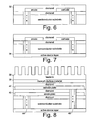
- FIG. 7 shows the formation of one or more active device layers 34 on the front side of the die.
- the active device layer will typically contain many active and passive components (not shown), some of which will be fabricated so as to be in electrical contact, through the vias, to the back side components such as the capacitor shown.
- FIG. 8 shows the addition of a thermal solution 36 such as a heat sink to the back side of the structure, typically with a layer of suitable thermal interface material 38 which improves contact between the surface of the outer diamond layer and the opposing surface of the heat sink.
- a thermal solution 36 such as a heat sink
- FIG. 8 also shows an alternative embodiment of the invention, in which two or more component layers are sandwiched between three or more diamond layers.
- One example of such a structure is a capacitor in which one of the anode 40 and the cathode 42 overlies the other, rather than the anode and cathode residing on the same layer as in FIG. 7 .
- This configuration may allow for very large surface areas of an anode plate and a cathode plate.
- the vias 44, 46 which connect to the anode and cathode, respectively, will be of different length, with one of them passing through and insulated from the other's plate.
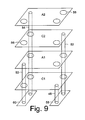
- FIG. 9 shows another embodiment of the multiple-layer structure, illustrating again the example of a capacitor.
- the diamond and other layers are omitted for the sake of illustration.
- the front side of the die should be understood to be downward in the drawing.
- a first capacitor includes a cathode plate C1 and an anode plate A1.
- a second capacitor overlies the first, and includes a cathode plate C2 and an anode plate A2.
- a first via 48 connects to the first capacitor's cathode.
- a second via 50 connects to the first capacitor's anode and passes through a hole in the first capacitor's cathode.
- a third via 52 connects to the second capacitor's cathode and passes through holes in the first capacitor's cathode and anode.
- a fourth via 54 connects to the second capacitor's anode and passes through holes in the first capacitor's cathode and anode and the second capacitor's cathode.
- dummy holes 56 may be desirable to construct dummy holes 56 in various of the cathodes and anodes, to equalize the surface areas of the anodes and cathodes, and so forth.
- the active component layers may be equipped with a cathode bus bar 58 an anode bus bar 60 to which the various cathodes and anodes are respectively coupled, to provide parallel connection to the various capacitors, effectively yielding one larger capacitor.
- FIG. 10 illustrates one embodiment of a capacitor structure which may be fabricated within a single back side component layer, such as that shown in FIG. 7 .
- the capacitor includes an anode 28 which has fingers 62 which are interlaces with the fingers 64 of the cathode 30.
- a first set of vias 24 connects to the anode, and a second set of vias 26 connects to the cathode.
- the skilled reader will appreciate that the vias are sized and spaced, and that the number, dimensions, spacing, and interlacing of the fingers are selected, according to the needs of the application at hand.
- FIG. 11 illustrates an alternative embodiment of a capacitor, in which the anode 28 and the cathode 30 are constructed as concentric rings or rectangles bearing first vias and second vias, respectively.
- FIG. 12 illustrates one example of an inductor 66 which can be formed within the back side diamond layers as a circular or rectangular or other suitable spiral of conductive material, with a pair of vias generally located at respective ends of the spiral.
- FIG. 13 illustrates one example of a resistor 72 which may be formed within the back side diamond layers.
- the resistor includes a first terminal 74 and a second terminal 76 coupled, respectively, to a first via 78 and a second via 80, and connected by a segment 82 of suitably sized and selected electrically resistive material.
- FIG. 14 illustrates one exemplary method 100 of manufacturing a semiconductor assembly according to this invention.
- Manufacturing starts (102) with a semiconductor substrate such as a wafer of silicon.
- a layer of high thermal conductivity material such as diamond is deposited (104) on the back side of the semiconductor substrate. Holes are drilled (106) or otherwise formed through the diamond and the substrate, and are insulated (108). Vias are formed (110) in the insulated holes.
- Back side components such as capacitors are formed (112) overlying the diamond, and in electrical connection with the vias. More diamond is deposited (114) overlying the earlier deposited diamond and the back side components.
- the process of forming back side components and encapsulating them in diamond can be repeated.
- the thickness of the semiconductor substrate can be reduced (116) if desired.
- Active devices are fabricated (118) on the front side of the semiconductor substrate.
- a thermal solution such as a heat sink is attached (120) to the back side, such as by connecting it to the diamond layer with a layer of thermal interface material.
- lateral interconnects to couple various ones of the back side components into networks, to extend vias or form new vias that are only on the back side, and so forth.
- back side components may be constructed within the limits of, and according to the teachings of, this patent. These components may be constructed as generally two-dimensional structures within a single component layer on the back side, or they may be constructed as three-dimensional structures within two or more component layers on the back side. In some embodiments, it may be desirable to fabricate some of their parts on the front side, as well. They may be constructed as discrete components, each having its own set of vias for connection to the front side, or they may be constructed as integrated component groups sharing sets of vias.
- any active components may be able to survive subsequent portions of the back side fabrication process.
- chemical vapor deposition of diamond is generally performed at temperatures of around 600°C.
- Materials other than diamond may be utilized as the high thermal conductivity, low electrical conductivity layers on the back side, but diamond is an especially well-suited material, as indicated above. Suitable materials will generally have thermal conductivity greater than 150 W/mK, electrical resistivity greater than 1.0E9 ⁇ -cm, and a dielectric constant above 5.0.
- drawings showing methods, and the written descriptions thereof, should also be understood to illustrate machine-accessible media having recorded, encoded, or otherwise embodied therein instructions, functions, routines, control codes, firmware, software, or the like, which, when accessed, read, executed, loaded into, or otherwise utilized by a machine, will cause the machine to perform the illustrated methods.
- Such media may include, by way of illustration only and not limitation: magnetic, optical, magneto-optical, or other storage mechanisms, fixed or removable discs, drives, tapes, semiconductor memories, organic memories, CD-ROM, CD-R, CD-RW, DVD-ROM, DVD-R, DVD-RW, Zip, floppy, cassette, reel-to-reel, or the like.
- the machines may alternatively include down-the-wire, broadcast, or other delivery mechanisms such as Internet, local area network, wide area network, wireless, cellular, cable, laser, satellite, microwave, or other suitable carrier means, over which the instructions etc. may be delivered in the form of packets, serial data, parallel data, or other suitable format.
- the machine may include, by way of illustration only and not limitation: microprocessor, embedded controller, PLA, PAL, FPGA, ASIC, computer, smart card, networking equipment, or any other machine, apparatus, system, or the like which is adapted to perform functionality defined by such instructions or the like.
- Such drawings, written descriptions, and corresponding claims may variously be understood as representing the instructions etc. taken alone, the instructions etc. as organized in their particular packet/serial/parallel/etc.
Landscapes
- Semiconductor Integrated Circuits (AREA)
- Cooling Or The Like Of Semiconductors Or Solid State Devices (AREA)
- Internal Circuitry In Semiconductor Integrated Circuit Devices (AREA)
Claims (15)
- Verfahren zum Herstellen einer Halbleitereinheit, wobei das Verfahren umfasst:Bilden einer ersten Materialschicht (16) mit hoher Wärmeleitfähigkeit auf einer Rückseite eines Halbleitersubstrats, wobei das Material mit hoher Wärmeleitfähigkeit eine Wärmeleitfähigkeit von mehr als 150 W/mK und einen spezifischen elektrischen Widerstand von mehr als 1E9 Ω · cm aufweist;Bilden einer Öffnung durch die erste Materialschicht mit hoher Wärmeleitfähigkeit unddurch das Halbleitersubstrat;Bilden einer Durchkontaktierung in der Öffnung;Bilden eines elektrischen Bauelements über der ersten Materialschicht (16) mit hoher Wärmeleitfähigkeit auf der Rückseite des Halbleitersubstrats und in einer elektrischen Verbindung mit der Durchkontaktierung;Bilden einer zweiten Materialschicht (32) mit hoher Wärmeleitfähigkeit über dem elektrischen Bauelement, sodass die Bauelemente zwischen der ersten und der zweiten Materialschicht eingebettet ist; undBilden einer Vorrichtung auf der Vorderseite des Halbleitersubstrats und mit einer elektrischen Verbindung mit der Durchkontaktierung.
- Verfahren nach Anspruch 1, das außerdem umfasst:Verbinden eines thermischen Elements mit der zweiten Materialschicht mit hoher Wärmeleitfähigkeit.
- Verfahren nach Anspruch 2, wobei das thermische Element eine Wärmesenke umfasst und das Verbinden der Wärmesenke mit der zweiten Materialschicht mit hoher Wärmeleitfähigkeit ein Platzieren einer Schicht aus einem thermischen Grenzschichtmaterial zwischen der Wärmesenke und der zweiten Materialschicht mit hoher Wärmeleitfähigkeit umfasst.
- Verfahren nach Anspruch 1, wobei das Bilden des elektrischen Bauelements umfasst: Bilden einer Anode und einer Kathode, und wobei das elektrische Bauelement einen Kondensator umfasst.
- Verfahren nach Anspruch 4, wobei das Bilden der Anode und der Kathode umfasst: Herstellen der Anode und der Kathode, sodass jede der beiden eine Vielzahl von Fingern aufweist, die mit den Fingern der jeweils anderen verschränkt sind.
- Verfahren nach Anspruch 5, wobei das Bilden der Anode und der Kathode umfasst:Bilden der Anode als eine Platte und Bilden der Kathode als eine Platte, wobei eine der Platten über der anderen Platte liegt; undBilden einer Zwischenschicht mit hoher Wärmeleitfähigkeit zwischen den Platten.
- Verfahren nach Anspruch 1, wobei das Material mit hoher Wärmeleitfähigkeit Diamant umfasst.
- Verfahren nach Anspruch 7, wobei das Bilden der Diamantschichten eine chemische Gasphasenabscheidung umfasst.
- Verfahren nach Anspruch 1, das außerdem, nach dem Bilden der zweiten Materialschicht mit hoher Wärmeleitfähigkeit und vor dem Bilden der Vorrichtung auf der Vorderseite, umfasst:Verringern einer Dicke des Halbleitersubstrats.
- Verfahren nach Anspruch 1, wobei:das Bilden der Öffnung ein Bilden einer Vielzahl von Öffnungen umfasst;das Bilden der Durchkontaktierung ein Bilden einer Vielzahl von Durchkontaktierungen in entsprechenden Öffnungen umfasst; unddas Bilden des elektrischen Bauelements ein Bilden einer Vielzahl von Vorrichtungen in einer elektrischen Verbindung mit entsprechenden Teilgruppen der Durchkontaktierungen umfasst.
- Verfahren nach Anspruch 1, wobei das Bilden des elektrischen Bauelements umfasst: Herstellen einer Spiralspule.
- Verfahren nach Anspruch 1, wobei das Bilden des elektrischen Bauelements umfasst: Herstellen eines Widerstands.
- Verfahren nach Anspruch 1, wobei das Material mit hoher Wärmeleitfähigkeit eine Wärmeleitfähigkeit von mehr als 200 W/mK aufweist.
- Verfahren nach Anspruch 1, wobei das Material mit hoher Wärmeleitfähigkeit eine Wärmeleitfähigkeit von mehr als 2000 W/mK aufweist.
- Verfahren nach Anspruch 14, wobei das Material mit hoher Wärmeleitfähigkeit einen spezifischen elektrischen Widerstand von mehr als 1E15 Ω · cm aufweist.
Applications Claiming Priority (3)
| Application Number | Priority Date | Filing Date | Title |
|---|---|---|---|
| US10/109,143 US6649937B2 (en) | 2002-03-26 | 2002-03-26 | Semiconductor device with components embedded in backside diamond layer |
| PCT/US2003/008592 WO2003083942A2 (en) | 2002-03-26 | 2003-03-19 | Semiconductor device with components embedded in backside diamond layer |
| US109143 | 2005-04-19 |
Publications (2)
| Publication Number | Publication Date |
|---|---|
| EP1490903A2 EP1490903A2 (de) | 2004-12-29 |
| EP1490903B1 true EP1490903B1 (de) | 2015-02-25 |
Family
ID=28453027
Family Applications (1)
| Application Number | Title | Priority Date | Filing Date |
|---|---|---|---|
| EP03723792.2A Expired - Lifetime EP1490903B1 (de) | 2002-03-26 | 2003-03-19 | Halbleitervorrichtung mit bauelementen, die in einer diamantschichtauf der rückseite der vorrichtung eingebettet sind |
Country Status (6)
| Country | Link |
|---|---|
| US (2) | US6649937B2 (de) |
| EP (1) | EP1490903B1 (de) |
| CN (1) | CN100347851C (de) |
| AU (1) | AU2003230702A1 (de) |
| TW (1) | TWI289349B (de) |
| WO (1) | WO2003083942A2 (de) |
Cited By (1)
| Publication number | Priority date | Publication date | Assignee | Title |
|---|---|---|---|---|
| EP3971964A3 (de) * | 2020-09-18 | 2022-03-30 | Intel Corporation | Kondensatoren und widerstände an direkten verbindungsschnittstellen in mikroelektronischen anordnungen |
Families Citing this family (16)
| Publication number | Priority date | Publication date | Assignee | Title |
|---|---|---|---|---|
| US6649937B2 (en) | 2002-03-26 | 2003-11-18 | Intel Corporation | Semiconductor device with components embedded in backside diamond layer |
| US7026711B2 (en) * | 2003-12-16 | 2006-04-11 | Taiwan Semiconductor Manufacturing Company, Ltd. | Thermal dispensing enhancement for high performance flip chip BGA (HPFCBGA) |
| US7064043B1 (en) * | 2004-12-09 | 2006-06-20 | Texas Instruments Incorporated | Wafer bonded MOS decoupling capacitor |
| US7310036B2 (en) | 2005-01-10 | 2007-12-18 | International Business Machines Corporation | Heat sink for integrated circuit devices |
| US8143654B1 (en) * | 2008-01-16 | 2012-03-27 | Triquint Semiconductor, Inc. | Monolithic microwave integrated circuit with diamond layer |
| US8816474B2 (en) * | 2008-08-07 | 2014-08-26 | Infineon Technologies Ag | Capacitor structure |
| US20100276701A1 (en) * | 2009-04-29 | 2010-11-04 | Hebert Francois | Low thermal resistance and robust chip-scale-package (csp), structure and method |
| TWI492851B (zh) * | 2009-07-27 | 2015-07-21 | Memjet Technology Ltd | 包含矽貫通(through-silicon)連接器之整合式列印頭 |
| US8232137B2 (en) | 2009-12-10 | 2012-07-31 | Intersil Americas Inc. | Heat conduction for chip stacks and 3-D circuits |
| US8859337B2 (en) * | 2009-12-15 | 2014-10-14 | Soitec | Thermal matching in semiconductor devices using heat distribution structures |
| FR2954828B1 (fr) * | 2009-12-30 | 2013-08-09 | Commissariat Energie Atomique | Capteur biologique a mesure electrochimique et/ou electrique et a electrode de diamant et circuit electronique integres |
| US20120306094A1 (en) * | 2011-06-06 | 2012-12-06 | Shahrazie Zainal Abu Bakar | Signal routing using through-substrate vias |
| US8810001B2 (en) | 2011-06-13 | 2014-08-19 | Mediatek Inc. | Seal ring structure with capacitor |
| US9123780B2 (en) | 2012-12-19 | 2015-09-01 | Invensas Corporation | Method and structures for heat dissipating interposers |
| US10658264B2 (en) * | 2017-09-01 | 2020-05-19 | Analog Devices, Inc. | Diamond-based heat spreading substrates for integrated circuit dies |
| EP4120377A1 (de) * | 2021-07-16 | 2023-01-18 | Murata Manufacturing Co., Ltd. | Diamantbasierte kondensatorstruktur |
Citations (5)
| Publication number | Priority date | Publication date | Assignee | Title |
|---|---|---|---|---|
| US4700457A (en) * | 1985-03-29 | 1987-10-20 | Mitsubishi Denki Kabushiki Kaisha | Method of making multilayer capacitor memory device |
| EP0663693A1 (de) * | 1993-11-30 | 1995-07-19 | Texas Instruments Incorporated | Integrierte Schaltung mit niedrigem Wärmewiderstand |
| US5811868A (en) * | 1996-12-20 | 1998-09-22 | International Business Machines Corp. | Integrated high-performance decoupling capacitor |
| US5955781A (en) * | 1998-01-13 | 1999-09-21 | International Business Machines Corporation | Embedded thermal conductors for semiconductor chips |
| US6292367B1 (en) * | 2000-06-22 | 2001-09-18 | International Business Machines Corporation | Thermally efficient semiconductor chip |
Family Cites Families (7)
| Publication number | Priority date | Publication date | Assignee | Title |
|---|---|---|---|---|
| US5683939A (en) * | 1993-04-02 | 1997-11-04 | Harris Corporation | Diamond insulator devices and method of fabrication |
| JP3309492B2 (ja) * | 1993-05-28 | 2002-07-29 | 住友電気工業株式会社 | 半導体装置用基板 |
| US5391914A (en) * | 1994-03-16 | 1995-02-21 | The United States Of America As Represented By The Secretary Of The Navy | Diamond multilayer multichip module substrate |
| JPH11307782A (ja) * | 1998-04-24 | 1999-11-05 | Semiconductor Energy Lab Co Ltd | 半導体装置およびその作製方法 |
| US6075712A (en) * | 1999-01-08 | 2000-06-13 | Intel Corporation | Flip-chip having electrical contact pads on the backside of the chip |
| US6509124B1 (en) * | 1999-11-10 | 2003-01-21 | Shin-Etsu Chemical Co., Ltd. | Method of producing diamond film for lithography |
| US6649937B2 (en) | 2002-03-26 | 2003-11-18 | Intel Corporation | Semiconductor device with components embedded in backside diamond layer |
-
2002
- 2002-03-26 US US10/109,143 patent/US6649937B2/en not_active Expired - Fee Related
-
2003
- 2003-03-19 CN CNB038113503A patent/CN100347851C/zh not_active Expired - Fee Related
- 2003-03-19 WO PCT/US2003/008592 patent/WO2003083942A2/en not_active Ceased
- 2003-03-19 EP EP03723792.2A patent/EP1490903B1/de not_active Expired - Lifetime
- 2003-03-19 TW TW092106045A patent/TWI289349B/zh not_active IP Right Cessation
- 2003-03-19 AU AU2003230702A patent/AU2003230702A1/en not_active Abandoned
- 2003-09-24 US US10/670,025 patent/US6913999B2/en not_active Expired - Fee Related
Patent Citations (5)
| Publication number | Priority date | Publication date | Assignee | Title |
|---|---|---|---|---|
| US4700457A (en) * | 1985-03-29 | 1987-10-20 | Mitsubishi Denki Kabushiki Kaisha | Method of making multilayer capacitor memory device |
| EP0663693A1 (de) * | 1993-11-30 | 1995-07-19 | Texas Instruments Incorporated | Integrierte Schaltung mit niedrigem Wärmewiderstand |
| US5811868A (en) * | 1996-12-20 | 1998-09-22 | International Business Machines Corp. | Integrated high-performance decoupling capacitor |
| US5955781A (en) * | 1998-01-13 | 1999-09-21 | International Business Machines Corporation | Embedded thermal conductors for semiconductor chips |
| US6292367B1 (en) * | 2000-06-22 | 2001-09-18 | International Business Machines Corporation | Thermally efficient semiconductor chip |
Cited By (2)
| Publication number | Priority date | Publication date | Assignee | Title |
|---|---|---|---|---|
| EP3971964A3 (de) * | 2020-09-18 | 2022-03-30 | Intel Corporation | Kondensatoren und widerstände an direkten verbindungsschnittstellen in mikroelektronischen anordnungen |
| US12266682B2 (en) | 2020-09-18 | 2025-04-01 | Intel Corporation | Capacitors and resistors at direct bonding interfaces in microelectronic assemblies |
Also Published As
| Publication number | Publication date |
|---|---|
| US20030183823A1 (en) | 2003-10-02 |
| US6649937B2 (en) | 2003-11-18 |
| EP1490903A2 (de) | 2004-12-29 |
| AU2003230702A1 (en) | 2003-10-13 |
| CN100347851C (zh) | 2007-11-07 |
| WO2003083942A3 (en) | 2004-02-26 |
| TWI289349B (en) | 2007-11-01 |
| CN1653611A (zh) | 2005-08-10 |
| US20040056272A1 (en) | 2004-03-25 |
| US6913999B2 (en) | 2005-07-05 |
| TW200403834A (en) | 2004-03-01 |
| WO2003083942A2 (en) | 2003-10-09 |
Similar Documents
| Publication | Publication Date | Title |
|---|---|---|
| EP1490903B1 (de) | Halbleitervorrichtung mit bauelementen, die in einer diamantschichtauf der rückseite der vorrichtung eingebettet sind | |
| US11417765B2 (en) | Quantum dot devices with fine-pitched gates | |
| JP4664013B2 (ja) | 高周波半導体装置の製造方法 | |
| KR101932660B1 (ko) | Tsv 구조를 구비한 집적회로 소자 및 그 제조 방법 | |
| US6249038B1 (en) | Method and structure for a semiconductor fuse | |
| CN110010561A (zh) | 一种多层芯片堆叠的射频结构及其制作方法 | |
| CN1751367B (zh) | 电容器及制造电容器的方法 | |
| CN107644837B (zh) | 用于三维存储器的晶圆三维集成引线工艺及其结构 | |
| US20070064395A1 (en) | Cooling system for a semiconductor device and method of fabricating same | |
| US20060220182A1 (en) | Semiconductor device | |
| US20110139497A1 (en) | Via Structure Integrated in Electronic Substrate | |
| US20190043953A1 (en) | Multi-spacers for quantum dot device gates | |
| WO2020005415A1 (en) | Quantum dot devices with multiple dielectrics around fins | |
| EP1145312B1 (de) | Verfahren zur herstellung von koaxialen verbindungsleitungen in einem cmos-prozess | |
| KR20030053047A (ko) | 반도체 장치 | |
| TW201044545A (en) | Techniques for placement of active and passive devices within a chip | |
| US20120009976A1 (en) | Recess gate transistor | |
| CN110010574A (zh) | 一种多层堆叠型纵向互联的射频结构及其制作方法 | |
| CN110010572A (zh) | 一种用于系统级大功率模组的大流量液冷散热器及其制作方法 | |
| US20040124446A1 (en) | PECVD air gap integration | |
| JPH11251316A (ja) | マルチチップ半導体装置の製造方法 | |
| US6432724B1 (en) | Buried ground plane for high performance system modules | |
| CN100444400C (zh) | 功率半导体器件及其方法 | |
| US20020055243A1 (en) | Gap-type metallic interconnect and method of manufacture | |
| CN106158829A (zh) | 包括限定空隙的材料的电子器件及其形成方法 |
Legal Events
| Date | Code | Title | Description |
|---|---|---|---|
| PUAI | Public reference made under article 153(3) epc to a published international application that has entered the european phase |
Free format text: ORIGINAL CODE: 0009012 |
|
| 17P | Request for examination filed |
Effective date: 20040930 |
|
| AK | Designated contracting states |
Kind code of ref document: A2 Designated state(s): AT BE BG CH CY CZ DE DK EE ES FI FR GB GR HU IE IT LI LU MC NL PT RO SE SI SK TR |
|
| AX | Request for extension of the european patent |
Extension state: AL LT LV MK |
|
| RIN1 | Information on inventor provided before grant (corrected) |
Inventor name: DUJARI, PRATEEK Inventor name: SEARLS, DAMION Inventor name: LIAN, BIN |
|
| 17Q | First examination report despatched |
Effective date: 20110721 |
|
| REG | Reference to a national code |
Ref country code: DE Ref legal event code: R079 Ref document number: 60347334 Country of ref document: DE Free format text: PREVIOUS MAIN CLASS: H01L0023373000 Ipc: H01L0021040000 |
|
| RIC1 | Information provided on ipc code assigned before grant |
Ipc: H01L 23/64 20060101ALI20140522BHEP Ipc: H01L 23/48 20060101ALI20140522BHEP Ipc: H01L 23/373 20060101ALI20140522BHEP Ipc: H01L 49/02 20060101ALI20140522BHEP Ipc: H01L 21/768 20060101ALI20140522BHEP Ipc: H01L 21/04 20060101AFI20140522BHEP |
|
| GRAP | Despatch of communication of intention to grant a patent |
Free format text: ORIGINAL CODE: EPIDOSNIGR1 |
|
| INTG | Intention to grant announced |
Effective date: 20140828 |
|
| GRAS | Grant fee paid |
Free format text: ORIGINAL CODE: EPIDOSNIGR3 |
|
| GRAA | (expected) grant |
Free format text: ORIGINAL CODE: 0009210 |
|
| AK | Designated contracting states |
Kind code of ref document: B1 Designated state(s): AT BE BG CH CY CZ DE DK EE ES FI FR GB GR HU IE IT LI LU MC NL PT RO SE SI SK TR |
|
| REG | Reference to a national code |
Ref country code: GB Ref legal event code: FG4D |
|
| REG | Reference to a national code |
Ref country code: CH Ref legal event code: EP |
|
| REG | Reference to a national code |
Ref country code: IE Ref legal event code: FG4D |
|
| REG | Reference to a national code |
Ref country code: DE Ref legal event code: R096 Ref document number: 60347334 Country of ref document: DE Effective date: 20150409 |
|
| REG | Reference to a national code |
Ref country code: AT Ref legal event code: REF Ref document number: 712624 Country of ref document: AT Kind code of ref document: T Effective date: 20150415 |
|
| REG | Reference to a national code |
Ref country code: NL Ref legal event code: VDEP Effective date: 20150225 |
|
| REG | Reference to a national code |
Ref country code: AT Ref legal event code: MK05 Ref document number: 712624 Country of ref document: AT Kind code of ref document: T Effective date: 20150225 |
|
| PG25 | Lapsed in a contracting state [announced via postgrant information from national office to epo] |
Ref country code: FI Free format text: LAPSE BECAUSE OF FAILURE TO SUBMIT A TRANSLATION OF THE DESCRIPTION OR TO PAY THE FEE WITHIN THE PRESCRIBED TIME-LIMIT Effective date: 20150225 Ref country code: SE Free format text: LAPSE BECAUSE OF FAILURE TO SUBMIT A TRANSLATION OF THE DESCRIPTION OR TO PAY THE FEE WITHIN THE PRESCRIBED TIME-LIMIT Effective date: 20150225 Ref country code: ES Free format text: LAPSE BECAUSE OF FAILURE TO SUBMIT A TRANSLATION OF THE DESCRIPTION OR TO PAY THE FEE WITHIN THE PRESCRIBED TIME-LIMIT Effective date: 20150225 |
|
| PG25 | Lapsed in a contracting state [announced via postgrant information from national office to epo] |
Ref country code: GR Free format text: LAPSE BECAUSE OF FAILURE TO SUBMIT A TRANSLATION OF THE DESCRIPTION OR TO PAY THE FEE WITHIN THE PRESCRIBED TIME-LIMIT Effective date: 20150526 Ref country code: AT Free format text: LAPSE BECAUSE OF FAILURE TO SUBMIT A TRANSLATION OF THE DESCRIPTION OR TO PAY THE FEE WITHIN THE PRESCRIBED TIME-LIMIT Effective date: 20150225 |
|
| PG25 | Lapsed in a contracting state [announced via postgrant information from national office to epo] |
Ref country code: NL Free format text: LAPSE BECAUSE OF FAILURE TO SUBMIT A TRANSLATION OF THE DESCRIPTION OR TO PAY THE FEE WITHIN THE PRESCRIBED TIME-LIMIT Effective date: 20150225 |
|
| PG25 | Lapsed in a contracting state [announced via postgrant information from national office to epo] |
Ref country code: EE Free format text: LAPSE BECAUSE OF FAILURE TO SUBMIT A TRANSLATION OF THE DESCRIPTION OR TO PAY THE FEE WITHIN THE PRESCRIBED TIME-LIMIT Effective date: 20150225 Ref country code: CZ Free format text: LAPSE BECAUSE OF FAILURE TO SUBMIT A TRANSLATION OF THE DESCRIPTION OR TO PAY THE FEE WITHIN THE PRESCRIBED TIME-LIMIT Effective date: 20150225 Ref country code: SK Free format text: LAPSE BECAUSE OF FAILURE TO SUBMIT A TRANSLATION OF THE DESCRIPTION OR TO PAY THE FEE WITHIN THE PRESCRIBED TIME-LIMIT Effective date: 20150225 Ref country code: DK Free format text: LAPSE BECAUSE OF FAILURE TO SUBMIT A TRANSLATION OF THE DESCRIPTION OR TO PAY THE FEE WITHIN THE PRESCRIBED TIME-LIMIT Effective date: 20150225 Ref country code: RO Free format text: LAPSE BECAUSE OF FAILURE TO SUBMIT A TRANSLATION OF THE DESCRIPTION OR TO PAY THE FEE WITHIN THE PRESCRIBED TIME-LIMIT Effective date: 20150225 |
|
| REG | Reference to a national code |
Ref country code: CH Ref legal event code: PL |
|
| REG | Reference to a national code |
Ref country code: DE Ref legal event code: R097 Ref document number: 60347334 Country of ref document: DE |
|
| PG25 | Lapsed in a contracting state [announced via postgrant information from national office to epo] |
Ref country code: MC Free format text: LAPSE BECAUSE OF FAILURE TO SUBMIT A TRANSLATION OF THE DESCRIPTION OR TO PAY THE FEE WITHIN THE PRESCRIBED TIME-LIMIT Effective date: 20150225 |
|
| PG25 | Lapsed in a contracting state [announced via postgrant information from national office to epo] |
Ref country code: IT Free format text: LAPSE BECAUSE OF FAILURE TO SUBMIT A TRANSLATION OF THE DESCRIPTION OR TO PAY THE FEE WITHIN THE PRESCRIBED TIME-LIMIT Effective date: 20150225 |
|
| PLBE | No opposition filed within time limit |
Free format text: ORIGINAL CODE: 0009261 |
|
| STAA | Information on the status of an ep patent application or granted ep patent |
Free format text: STATUS: NO OPPOSITION FILED WITHIN TIME LIMIT |
|
| REG | Reference to a national code |
Ref country code: IE Ref legal event code: MM4A |
|
| GBPC | Gb: european patent ceased through non-payment of renewal fee |
Effective date: 20150525 |
|
| PG25 | Lapsed in a contracting state [announced via postgrant information from national office to epo] |
Ref country code: IE Free format text: LAPSE BECAUSE OF NON-PAYMENT OF DUE FEES Effective date: 20150319 Ref country code: LI Free format text: LAPSE BECAUSE OF NON-PAYMENT OF DUE FEES Effective date: 20150331 Ref country code: CH Free format text: LAPSE BECAUSE OF NON-PAYMENT OF DUE FEES Effective date: 20150331 |
|
| 26N | No opposition filed |
Effective date: 20151126 |
|
| REG | Reference to a national code |
Ref country code: FR Ref legal event code: ST Effective date: 20160108 |
|
| PG25 | Lapsed in a contracting state [announced via postgrant information from national office to epo] |
Ref country code: SI Free format text: LAPSE BECAUSE OF FAILURE TO SUBMIT A TRANSLATION OF THE DESCRIPTION OR TO PAY THE FEE WITHIN THE PRESCRIBED TIME-LIMIT Effective date: 20150225 |
|
| PG25 | Lapsed in a contracting state [announced via postgrant information from national office to epo] |
Ref country code: GB Free format text: LAPSE BECAUSE OF NON-PAYMENT OF DUE FEES Effective date: 20150525 |
|
| PGFP | Annual fee paid to national office [announced via postgrant information from national office to epo] |
Ref country code: DE Payment date: 20160315 Year of fee payment: 14 |
|
| PG25 | Lapsed in a contracting state [announced via postgrant information from national office to epo] |
Ref country code: BE Free format text: LAPSE BECAUSE OF FAILURE TO SUBMIT A TRANSLATION OF THE DESCRIPTION OR TO PAY THE FEE WITHIN THE PRESCRIBED TIME-LIMIT Effective date: 20150225 Ref country code: FR Free format text: LAPSE BECAUSE OF NON-PAYMENT OF DUE FEES Effective date: 20150427 |
|
| PG25 | Lapsed in a contracting state [announced via postgrant information from national office to epo] |
Ref country code: BG Free format text: LAPSE BECAUSE OF FAILURE TO SUBMIT A TRANSLATION OF THE DESCRIPTION OR TO PAY THE FEE WITHIN THE PRESCRIBED TIME-LIMIT Effective date: 20150225 Ref country code: HU Free format text: LAPSE BECAUSE OF FAILURE TO SUBMIT A TRANSLATION OF THE DESCRIPTION OR TO PAY THE FEE WITHIN THE PRESCRIBED TIME-LIMIT; INVALID AB INITIO Effective date: 20030319 |
|
| PG25 | Lapsed in a contracting state [announced via postgrant information from national office to epo] |
Ref country code: CY Free format text: LAPSE BECAUSE OF FAILURE TO SUBMIT A TRANSLATION OF THE DESCRIPTION OR TO PAY THE FEE WITHIN THE PRESCRIBED TIME-LIMIT Effective date: 20150225 |
|
| PG25 | Lapsed in a contracting state [announced via postgrant information from national office to epo] |
Ref country code: PT Free format text: LAPSE BECAUSE OF FAILURE TO SUBMIT A TRANSLATION OF THE DESCRIPTION OR TO PAY THE FEE WITHIN THE PRESCRIBED TIME-LIMIT Effective date: 20150625 |
|
| PG25 | Lapsed in a contracting state [announced via postgrant information from national office to epo] |
Ref country code: TR Free format text: LAPSE BECAUSE OF FAILURE TO SUBMIT A TRANSLATION OF THE DESCRIPTION OR TO PAY THE FEE WITHIN THE PRESCRIBED TIME-LIMIT Effective date: 20150225 |
|
| REG | Reference to a national code |
Ref country code: DE Ref legal event code: R119 Ref document number: 60347334 Country of ref document: DE |
|
| PG25 | Lapsed in a contracting state [announced via postgrant information from national office to epo] |
Ref country code: LU Free format text: LAPSE BECAUSE OF NON-PAYMENT OF DUE FEES Effective date: 20150319 |
|
| PG25 | Lapsed in a contracting state [announced via postgrant information from national office to epo] |
Ref country code: DE Free format text: LAPSE BECAUSE OF NON-PAYMENT OF DUE FEES Effective date: 20171003 |