EP1489628A1 - Conductive glass and photoelectric conversion device using same - Google Patents
Conductive glass and photoelectric conversion device using same Download PDFInfo
- Publication number
- EP1489628A1 EP1489628A1 EP03720892A EP03720892A EP1489628A1 EP 1489628 A1 EP1489628 A1 EP 1489628A1 EP 03720892 A EP03720892 A EP 03720892A EP 03720892 A EP03720892 A EP 03720892A EP 1489628 A1 EP1489628 A1 EP 1489628A1
- Authority
- EP
- European Patent Office
- Prior art keywords
- electrically conductive
- film
- grid
- transparent electrically
- conductive glass
- Prior art date
- Legal status (The legal status is an assumption and is not a legal conclusion. Google has not performed a legal analysis and makes no representation as to the accuracy of the status listed.)
- Granted
Links
Images


Classifications
-
- H—ELECTRICITY
- H01—ELECTRIC ELEMENTS
- H01B—CABLES; CONDUCTORS; INSULATORS; SELECTION OF MATERIALS FOR THEIR CONDUCTIVE, INSULATING OR DIELECTRIC PROPERTIES
- H01B5/00—Non-insulated conductors or conductive bodies characterised by their form
- H01B5/14—Non-insulated conductors or conductive bodies characterised by their form comprising conductive layers or films on insulating-supports
-
- H—ELECTRICITY
- H01—ELECTRIC ELEMENTS
- H01G—CAPACITORS; CAPACITORS, RECTIFIERS, DETECTORS, SWITCHING DEVICES, LIGHT-SENSITIVE OR TEMPERATURE-SENSITIVE DEVICES OF THE ELECTROLYTIC TYPE
- H01G9/00—Electrolytic capacitors, rectifiers, detectors, switching devices, light-sensitive or temperature-sensitive devices; Processes of their manufacture
- H01G9/20—Light-sensitive devices
- H01G9/2068—Panels or arrays of photoelectrochemical cells, e.g. photovoltaic modules based on photoelectrochemical cells
-
- B—PERFORMING OPERATIONS; TRANSPORTING
- B32—LAYERED PRODUCTS
- B32B—LAYERED PRODUCTS, i.e. PRODUCTS BUILT-UP OF STRATA OF FLAT OR NON-FLAT, e.g. CELLULAR OR HONEYCOMB, FORM
- B32B17/00—Layered products essentially comprising sheet glass, or glass, slag, or like fibres
- B32B17/06—Layered products essentially comprising sheet glass, or glass, slag, or like fibres comprising glass as the main or only constituent of a layer, next to another layer of a specific material
-
- H—ELECTRICITY
- H01—ELECTRIC ELEMENTS
- H01G—CAPACITORS; CAPACITORS, RECTIFIERS, DETECTORS, SWITCHING DEVICES, LIGHT-SENSITIVE OR TEMPERATURE-SENSITIVE DEVICES OF THE ELECTROLYTIC TYPE
- H01G9/00—Electrolytic capacitors, rectifiers, detectors, switching devices, light-sensitive or temperature-sensitive devices; Processes of their manufacture
- H01G9/20—Light-sensitive devices
- H01G9/2027—Light-sensitive devices comprising an oxide semiconductor electrode
- H01G9/2031—Light-sensitive devices comprising an oxide semiconductor electrode comprising titanium oxide, e.g. TiO2
-
- H—ELECTRICITY
- H01—ELECTRIC ELEMENTS
- H01M—PROCESSES OR MEANS, e.g. BATTERIES, FOR THE DIRECT CONVERSION OF CHEMICAL ENERGY INTO ELECTRICAL ENERGY
- H01M14/00—Electrochemical current or voltage generators not provided for in groups H01M6/00 - H01M12/00; Manufacture thereof
-
- H—ELECTRICITY
- H01—ELECTRIC ELEMENTS
- H01M—PROCESSES OR MEANS, e.g. BATTERIES, FOR THE DIRECT CONVERSION OF CHEMICAL ENERGY INTO ELECTRICAL ENERGY
- H01M14/00—Electrochemical current or voltage generators not provided for in groups H01M6/00 - H01M12/00; Manufacture thereof
- H01M14/005—Photoelectrochemical storage cells
-
- H—ELECTRICITY
- H10—SEMICONDUCTOR DEVICES; ELECTRIC SOLID-STATE DEVICES NOT OTHERWISE PROVIDED FOR
- H10F—INORGANIC SEMICONDUCTOR DEVICES SENSITIVE TO INFRARED RADIATION, LIGHT, ELECTROMAGNETIC RADIATION OF SHORTER WAVELENGTH OR CORPUSCULAR RADIATION
- H10F10/00—Individual photovoltaic cells, e.g. solar cells
-
- H—ELECTRICITY
- H10—SEMICONDUCTOR DEVICES; ELECTRIC SOLID-STATE DEVICES NOT OTHERWISE PROVIDED FOR
- H10F—INORGANIC SEMICONDUCTOR DEVICES SENSITIVE TO INFRARED RADIATION, LIGHT, ELECTROMAGNETIC RADIATION OF SHORTER WAVELENGTH OR CORPUSCULAR RADIATION
- H10F77/00—Constructional details of devices covered by this subclass
- H10F77/20—Electrodes
- H10F77/244—Electrodes made of transparent conductive layers, e.g. transparent conductive oxide [TCO] layers
-
- H—ELECTRICITY
- H10—SEMICONDUCTOR DEVICES; ELECTRIC SOLID-STATE DEVICES NOT OTHERWISE PROVIDED FOR
- H10K—ORGANIC ELECTRIC SOLID-STATE DEVICES
- H10K30/00—Organic devices sensitive to infrared radiation, light, electromagnetic radiation of shorter wavelength or corpuscular radiation
- H10K30/80—Constructional details
- H10K30/81—Electrodes
- H10K30/82—Transparent electrodes, e.g. indium tin oxide [ITO] electrodes
- H10K30/83—Transparent electrodes, e.g. indium tin oxide [ITO] electrodes comprising arrangements for extracting the current from the cell, e.g. metal finger grid systems to reduce the serial resistance of transparent electrodes
-
- Y—GENERAL TAGGING OF NEW TECHNOLOGICAL DEVELOPMENTS; GENERAL TAGGING OF CROSS-SECTIONAL TECHNOLOGIES SPANNING OVER SEVERAL SECTIONS OF THE IPC; TECHNICAL SUBJECTS COVERED BY FORMER USPC CROSS-REFERENCE ART COLLECTIONS [XRACs] AND DIGESTS
- Y02—TECHNOLOGIES OR APPLICATIONS FOR MITIGATION OR ADAPTATION AGAINST CLIMATE CHANGE
- Y02E—REDUCTION OF GREENHOUSE GAS [GHG] EMISSIONS, RELATED TO ENERGY GENERATION, TRANSMISSION OR DISTRIBUTION
- Y02E10/00—Energy generation through renewable energy sources
- Y02E10/50—Photovoltaic [PV] energy
- Y02E10/542—Dye sensitized solar cells
Definitions
- the present invention relates to a electrically conductive glass used in a dye-sensitized solar cell or other photoelectric conversion clement, having high electrical conductivity and transparency, which is able to reduce leakage current when used in a photoelectric conversion element.
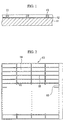
- FIG 1 shows an electrically conductive glass
- reference symbol 11 indicates a glass plate.
- This glass plate 11 is made of soda glass, heat-resistant glass, or quartz glass and so forth having a thickness of about 1 to 5 mm.
- This transparent electrically conductive film 12 is composed of a thin film of tin-doped indium oxide (ITO), fluorine-doped tin oxide (FTO) and so forth that is both transparent and electrically conductive, has a thickness of about 0.2 to 1 ⁇ m, and is formed by a thin film formation method such as sputtering or CVD.
- ITO tin-doped indium oxide
- FTO fluorine-doped tin oxide
- a grid 13 composed of a metal film is sealed on this transparent electrically conductive film 12.
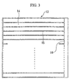
- planar shape of this grid 13 may be, for example, in the form of a lattice as shown in FIG 2 or in the form of the teeth of a comb as shown in FIG 3.
- a countless number of rectangular openings 14, 14 ⁇ having a width of 450 to 2000 ⁇ m and length of 2000 to 20000 ⁇ m are formed, and the width of line 15, which is composed of a metal film extending vertically and horizontally to form a matrix is 10 to 1000 ⁇ m.
- a wide collecting electrode 16 for collecting electricity is formed extending in the vertical direction on one side.
- a countless number of lines 15, 15 ⁇ which form the teeth of a comb, are composed of a metal film and have a width of 10 to 1000 ⁇ m, are formed mutually in parallel at an interval of 450 to 2000 ⁇ m, a countless number of openings 14, 14 ⁇ are formed, and a wide collecting electrode 16 for collecting electricity is formed on one of its ends.
- This grid 13 is formed by a method such as a plating method and so forth, which is composed of a metal such as gold, silver, platinum, chromium, or nickel, or an alloy of two or more metals thereof, and the thickness of lines 15 is 1 to 20 ⁇ m, preferably 3 to 10 ⁇ m.
- the numerical aperture of this grid 13 is made to be 90 to 99%.
- the numerical aperture referred to here is defined as the ratio of the total surface area of lines 15 to the unit surface area.
- the total surface resistance of transparent electrically conductive film 12 and the grid 13 (referred to as the sheet resistance) over the entire surface of this electrically conductive glass is 1 to 0.01 ⁇ / ⁇ , and is roughly 1/10 to 1/100 of that of transparent electrically conductive glass provided with a transparent electrically conductive film such as an ITO or FTO film. Consequently, this electrically conductive glass can be said to exhibit extremely high electrical conductivity.
- the entire surface of this type of electrically conductive glass has a high average optical transmittance ranging over the whole surface. Namely, this is because, since the electrically conductivity is improved considerably by the presence of the grid 13, the thickness of the transparent electrically conductive film 12 can be reduced, and since the numerical aperture of the grid 13 is 90 to 99%, there is hardly any blocking of incident light by the presence of the grid 13.
- the electrically conductive glass of this invention of a prior application has high electrical conductivity and transparency, and a dye-sensitized solar cell in which it is used has possibilities to exhibit a high photoelectric conversion efficiency.
- a barrier layer which is composed of a semiconductor or insulator such as titanium oxide or tin oxide, is further provided at the interface between the grid 13 and the electrolyte, and this barrier is expected to be able to inhibit leakage current that flows from the grid 13 towards the electrolyte.
- This barrier layer can be formed by a method such as sputtering, complex sintering, spray pyrolysis and CVD.
- this barrier layer is also formed on the transparent electrically conductive film 12 other than the grid 13, when used in a dye-sensitized solar cell, the electrons generated in the oxide semiconductor porous film are obstructed from flowing to the transparent electrically conductive film 12, thereby causing a decrease in the amount of generated current or decrease in the fill factor (FF).
- FF fill factor
- the barrier layer should only be formed on the grid 13 in order to resolve this problem, the problem of the pinholes remains, and their formation requires a bothersome process such as photolithography, thereby making this disadvantageous in terms of cost.
- nickel is primarily used for the metal serving as the grid 13 in consideration of the manner in which it is formed.
- the nickel serving as the grid 13 penetrates into the transparent electrically conductive film 12 resulting in deterioration of the transparent electrically conductive film 12 during standing for a long period of time or when subjected to a heat treatment.
- an object of the present invention is to provide electrically conductive glass in which a transparent electrically conductive film is provided on a glass and a grid includes a metal film is provided on this transparent electrically conductive film; wherein, when this electrically conductive glass is assembled in a dye-sensitized solar cell or other photoelectric conversion element, the generation of a leakage current flowing from the grid to an electrolyte as well as a leakage current flowing from the transparent electrically conductive film to the electrolyte are prevented.
- the invention as claimed in claim 1 is an electrically conductive glass including a transparent electrically conductive film provided on a glass surface, and a grid including a passivated metal film provided on the transparent electrically conductive film.
- the invention as claimed in claim 2 is the electrically conductive glass according to claim 1 wherein the passivated metal is nickel, chromium, or cobalt, or an alloy of two or more species thereof.
- the invention as claimed in claim 3 is the electrically conductive glass according to claim 1 or 2 wherein a thickness of an oxide film formed on the surface of the grid including a passivated metal film is 10 to 500 nm.
- the invention as claimed in claim 4 is the electrically conductive glass according to any of claims 1 to 3 wherein only the surface of the grid is of the passivated metal.
- the invention as claimed in claim 5 is a method of manufacturing an electrically conductive glass including forming a transparent electrically conductive film on a glass surface, and when forming a grid including a passivated metal film on the transparent electrically conductive film and obtaining an electrically conductive glass, heat-treating the grid at 120 to 550°C in an oxygen atmosphere.
- the invention as claimed in claim 6 is an electrically conductive glass including a transparent electrically conductive film provided on a glass surface, a diffusion-preventing film provided on the transparent electrically conductive film, and a grid including a metal film containing nickel provided on the diffusion-preventing film.
- the invention as claimed in claim 7 is an electrically conductive glass including a transparent electrically conductive film provided on a glass surface, a grid including a metal film containing nickel provided on the transparent electrically conductive film, and a diffusion-preventing film provided on the grid and on the transparent electrically conductive film.
- the invention as claimed in claim 8 is the electrically conductive glass according to claim 6 or 7 wherein the diffusion-preventing film is formed from titanium, titanium oxide, niobium, or chromium.
- the invention as claimed in claim 9 is the electrically conductive glass according to claim 8 wherein a thickness of the titanium oxide that forms the diffusion-preventing film is 0.1 ⁇ m or less.
- the invention as claimed in claim 10 is a photoelectric conversion element wherein the electrically conductive glass according to any of claims 1, 2, 3, 4, 6, 7, 8, or 9 is used.
- the invention as claimed in claim 11 is the photoelectric conversion element according to claim 10 which is a dye-sensitized solar cell.
- a metal film serving as a grid 13 is formed from a passivated metal on an electrically conductive glass having, for example, the structure shown in Figs. 1 to 3.
- the passivated metal in the present invention refers to a metal capable of forming a fine oxide film on its surface in air or other oxidizing atmosphere, an alloy of these passivated metals, or an alloy of this passivated metal and another metal. More specifically, examples of passivated metals include aluminum, chromium, nickel, cobalt, titanium, manganese, molybdenum, tungsten, zinc, tin, as well as alloys such as nickel-chromium alloy, iron-nickel-chromium alloy, aluminum-tungsten alloy, nickel-zinc alloy, and silver-zinc alloy.
- a plating additive method is primarily employed as a method for forming the grid 13, among those metals, metals that can be plated are preferable, and further, since a low electrical resistance of grid 13 is preferable, metals having low volume resistivity such as nickel, chromium, cobalt, or their metal alloys are the most preferable.
- the grid 13 may have a structure in which an inner layer includes a metal other than a passivated metal such as gold, silver, or platinum, while the surface includes the aforementioned passivated metal.
- the grid 13 in which only the surface is of a passivated metal can be formed by, for example, a method in which a grid precursor including a metal other than a passivated metal such as gold, silver, or platinum is first produced on a transparent electrically conductive film 12 by plating and so forth, followed by performing an electroless plating on this grid precursor to coat the precursor grid with a passivated metal such as nickel, chromium, or tin.
- a plating additive method is preferable for the formation of the grid 13 including a passivated metal as previously described, it can also be formed by various types of thin film formation methods such as sputtering or vapor deposition.
- an electrically insulated oxide film is formed naturally on the surface of the grid 13 immediately after its formation, and this insulated oxide film serves as a barrier layer that functions as a leakage current preventive layer.
- this electrically conductive glass since the electrically conductive glass is exposed to high temperatures when an oxide semiconductor porous film including titanium oxide and so forth is formed on the electrically conductive glass by the sintering method, an oxide film having an adequate thickness is formed on the surface of the grid 13 which serves as an effective barrier.
- the oxide film may preferably be formed aggressively by performing a heat treatment in an oxygen atmosphere.
- This heat treatment is carried out under conditions of a temperature of 120 to 550°C and preferably 150 to 450°C, and a treatment duration of 5 to 120 minutes and preferably 10 to 90 minutes, while the heat treatment varying according to the type of passivated metal. If the temperature is lower than 120°C and the treatment duration is less than 5 minutes, it is not possible to obtain the oxide film of adequate thickness, while if the temperature exceeds 550°C, the glass plate 11 itself ends up melting. If the treatment duration exceeds 120 minutes, it essentially becomes superfluous, thereby making this uneconomical.
- this heat treatment can also be carried out by baking at the same temperature and treatment duration when forming the oxide semiconductor porous film including titanium oxide and so forth by baking.
- the thickness of an oxide film formed in this manner is roughly 10 to 500 nm. If the thickness is less than 100 nm, leakage current preventive effects are unable to be obtained, while if the thickness exceeds 500 nm, the desired effects reach a maximum resulting in prolongation of the treatment duration for forming the oxide film, thereby making this impractical.
- FIG. 4 shows an example of a dye-sensitized solar cell in the form of a photoelectric conversion element in which this type of electrically conductive glass is used.
- reference symbol 21 is the electrically conductive glass shown in Figs. 1 to 3.
- An oxide semiconductor porous film 22 is provided on the grid 13 including a passivated metal of this electrically conductive glass 21.
- This oxide semiconductor porous film 22 is a porous body including metal oxide fine particles which are connected with each other and demonstrate semiconductivity such as titanium oxide, tin oxide, tungsten oxide, zinc oxide, zirconium oxide, or niobium oxide and having countless fine pores inside and fine irregularities in its surface, and having a thickness of 5 to 50 ⁇ m.
- this oxide semiconductor porous film 22 fills in the openings 14 of grid 13, covers the entire surface of grid 13 and is integrally bonded with the grid 13.
- this oxide semiconductor porous film 22 is carried out using a method, for example, in which a colloidal liquid or dispersion in which is dispersed fine particles of the aforementioned metal oxide having an average particle diameter of 5 to 50 nm is coated onto the surface of the grid 13 by a coating method such as screen printing, ink jet printing, roll coating, doctor coating, or spray coating followed by sintering at 300 to 800°C.
- a coating method such as screen printing, ink jet printing, roll coating, doctor coating, or spray coating followed by sintering at 300 to 800°C.
- a photosensitive dye is adsorbed to this oxide semiconductor porous film 22.
- Ruthenium complexes containing ligands such as a bipyridine structure or terpyridine structure, metal complexes such as porphyrin or phthalocyanine, or organic dyes such as eosin, rhodamine, or merocyanine are used for this photosensitive dye, and it can be suitably selected according to its application, type of metal oxide semiconductor, and so forth.
- reference symbol 23 indicates a counter electrode.
- a counter electrode in which an electrically conductive thin film 23b composed of platinum or gold and so forth is formed by vapor deposition or sputtering deposition and so forth on the surface of a metal-clad of a metal-clad laminated film 23a in which the metal-clad such as a copper foil or a nickel foil is laminated on one side of a polyimide, polyethylene terephthalate, or other plastic film, and in the dye-sensitized solar cell of the present example, the electrically conductive thin film 23b is arranged so as to be on the inside of the solar cell.
- a counter electrode in which an electrically conductive film 23b made of platinum, gold, carbon, and so forth is formed on an electrically conductive substrate such as a metal plate or a non-electrically conductive substrate 23a such as a glass plate may also be used for counter electrode 23.
- an electrically conductive film 23b made of platinum, gold, carbon, and so forth is formed on an electrically conductive substrate such as a metal plate or a non-electrically conductive substrate 23a such as a glass plate may also be used for counter electrode 23.
- a platinum or other electrically conductive film can be formed by vapor deposition or sputtering directly thereon and this electrically conductive film can also be used as counter electrode 23.
- An electrolyte is filled into the space between this counter electrode 23 and the oxide semiconductor porous film 22 of the electrically conductive glass 21 to form an electrolyte layer.
- this electrolyte is a non-aqueous electrolyte that contains a redox pair.
- solvents that are used include acetonitrile, methoxyacetonitrile, propionitrile, ethylene carbonate, propylene carbonate, and ⁇ -butyrolactone.
- Combinations such as iodine and iodide ion or bromine and bromide ion can be selected for the redox pair, and examples of counter ions that can be used in the case of adding those combinations in the form of a salt include lithium ion, tetraalkyl ion, and imidazolium ion.
- iodine and so forth may also be added as necessary.
- this electrolyte may also be used in the form of a solid by gelling with a suitable gelling agent.
- a hole transport layer composed of p-type semiconductor may also be used.
- a monovalent copper compound such as copper iodide or copper thiocyanide or an electrically conductive polymer such as polypyrrole can be used for this p-type semiconductor, with copper iodide being particularly preferable.
- the grid 13 including a film of a passivated metal is provided on the transparent electrically conductive film 12 in this type of electrically conductive glass, it exhibits both high electrical conductivity and high transparency.
- the grid 13 is including the passivated metal, a fine, insulated oxide film is formed on its surface, and this oxide film functions as a barrier layer that prevents the generation of leakage current.
- erosion of the grid 13 by electrolyte can also be prevented by this oxide film.
- this oxide film is extremely fine, there is hardly any formation of pin holes in the coating film, thereby eliminating the risk of leakage current caused by the presence of pin holes.
- a special barrier layer is not required to be formed on the grid 13, there is the advantage of improved workability and reduced costs.
- FIG. 5 is a schematic cross-sectional view showing a second example of the electrically conductive glass of the present invention.
- the same reference symbols are used to indicate those constituent features that are the same as the constituent features of the electrically conductive glass shown in Figs. 1 to 3, and their explanations are omitted.
- the electrically conductive glass of this example has a diffusion-preventing film 31 provided on a transparent electrically conductive film 12, and a grid 13 including a film of a metal containing nickel provided on this diffusion-preventing film 31 in the electrically conductive glass having, for example, the structure shown in Figs. 1 to 3.
- Diffusion-preventing film 31 is provided between the transparent electrically conductive film 12 and the grid 13 to prevent the penetration and diffusion of nickel contained in the metal film that forms the grid 13 into an FTO and so forth that forms transparent electrically conductive film 12, and although any material can be used if it is highly adhesive with ITO, FTO, and so forth and has high adhesion with other metals, it is preferably formed from, for example, titanium, titanium oxide, niobium, or chromium.
- Titanium oxide is particularly preferable since it has superior weather resistance, heat resistance, and chemical resistance, has extremely high chemical stability, and does not have an effect on power generation characteristics (such as photoelectric conversion efficiency) when the electrically conductive glass is applied to a dye-sensitized solar cell, while titanium is even more preferable since it becomes stable titanium oxide as a result of sintering.
- a thickness of diffusion-preventing film 31 is 0.005 to 0.2 ⁇ m and preferably 0.01 to 0.03 ⁇ m. If the thickness of diffusion-preventing film 31 is less than 0.005 ⁇ m, penetration and diffusion of the nickel contained in the metal film that forms the grid 13 into the FTO and so forth that forms transparent electrically conductive film 12 cannot be prevented. On the other hand, if the thickness of diffusion-preventing film 31 exceeds 0.2 ⁇ m, there is the risk of a decrease in the photoelectric conversion efficiency in the case of applying the electrically conductive glass to a dye-sensitized solar cell. In particular, in the case in which the diffusion-preventing film 31 is formed with titanium oxide, its thickness is preferably 0.1 ⁇ m or less and more preferably 0.01 to 0.03 ⁇ m.
- the diffusion-preventing film 31 is formed from titanium oxide, there is no deterioration in power generation characteristics even if its thickness is extremely thin, and the nickel contained in the metal film that forms the grid 13 can be prevented from penetrating and diffusing into the FTO and so forth that forms transparent electrically conductive film 12.
- a transparent electrically conductive glass 32 is prepared, wherein a transparent electrically conductive film 12, such as ITO or FTO, and so forth, is provided on the glass substrate 11 shown in FIG. 6.
- a transparent electrically conductive film 12 such as ITO or FTO, and so forth.
- This type of transparent electrically conductive glass 32 is available commercially, and can be acquired from such firms as Asahi Glass Co., Ltd. and Nippon Sheet Glass Co., Ltd..
- the surface of transparent electrically conductive film 12 of this transparent electrically conductive glass 32 is cleaned by plasma cleaning, and a seed layer 33 is provided thereon by sputtering silver, chromium, nickel, or gold.
- a seed layer 33 is provided thereon by sputtering silver, chromium, nickel, or gold.
- the surface of this seed layer 33 is cleaned by plasma cleaning, and a diffusion-preventing layer 31 is formed thereon by sputtering titanium, titanium oxide, niobium, or chromium.
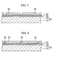
- a dry resist film is placed on this diffusion-preventing film 31 followed by exposure and development to form a mask 34 having a pattern in the planar shape of the grid 13 as shown in FIG. 7, and additionally followed by baking and an activation treatment.
- nickel plating is performed on the diffusion-preventing layer 31 that is exposed through the mask 34 by using the diffusion-preventing layer 31 as one of electrodes to form a nickel layer 35 to serve as the grid 13 as shown in FIG. 8.
- a method in which strike plating is first performed at a high current density followed by electrolytic nickel plating at a normal current density is preferable for improving adhesion.
- electrolytic nickel plating solutions used for this electrolytic nickel plating include nickel sulfamate using sulfamic acid as a solvent, Watt's bath (nickel sulfate) and chloride bath (nickel chloride).
- the remaining mask 34 is peeled off and removed and the entire structure is heated to anneal the nickel layer 35 serving as the grid 13, the diffusion-preventing film 31 beneath this nickel layer 35, and the seed layer 33 into an alloy. Furthermore, the diffusion-preventing layer 31 and the seed layer 33 beneath the mask 34 may be suitably removed by etching.
- the electrically conductive glass having the structure shown in FIG. 5 is obtained by cleaning the entire structure.
- the grid 13 may be formed by processing the nickel layer 35 to a desired shape by dry etching after forming this nickel layer 35 over the entire surface of the diffusion-preventing film 31 without providing the mask 34 as previously described.
- etching ended up being performed excessively to remove unevenness in the case of unevenness in the thickness of the nickel layer or unevenness of the etching, thereby resulting in deterioration of the transparent electrically conductive film caused by over-etching at portions where the nickel layer had already been removed.
- the ratio of the etching speed of titanium to the etching speed of nickel is 1/5, even if there is unevenness in the thickness of the nickel layer or unevenness of the etching, etching stops at the titanium layer (the diffusion-preventing film) until the nickel layer is completely removed, thereby preventing over-etching of the transparent electrically conductive film.
- the diffusion-preventing film 31 including titanium and so forth is provided between the transparent electrically conductive film 12 and the nickel layer 35, there is no deterioration of the transparent electrically conductive film 12 caused by this over-etching.
- the diffusion-preventing film 31 should at least be provided only between the transparent electrically conductive film 12 and the nickel layer 35, it is preferably provided over the entire surface of the transparent electrically conductive film 12.
- the grid 13 may be formed by processing the nickel layer 35 to a desired shape by dry etching after forming this nickel layer 35 over the entire surface of the diffusion-preventing film 31 without providing a mask 34. Consequently, if the diffusion-preventing film 35 is only formed between the transparent electrically conductive film 12 and the nickel layer 35 serving as the grid 13, since the transparent electrically conductive film 12 and the nickel layer 35 that is subsequently removed by etching temporarily make contact, thereby resulting in the risk of the nickel that forms the nickel layer 35 penetrating and diffusing into the FTO and so forth that forms the transparent electrically conductive film 12.
- the diffusion-preventing film 31 preferably is provided over the entire surface of the transparent electrically conductive film 12.
- the diffusion-preventing film 31 is provided on the transparent electrically conductive film 12 that is provided on the surface of glass plate 11, and although the grid 13 is provided on this diffusion-preventing film 31, it is not limited to this.
- the grid 13 is provided on the transparent electrically conductive film 12 that is provided on the surface of the glass plate 11, and the diffusion-preventing film 31 is provided on this grid 13 and on the transparent electrically conductive film 12.
- a dry resist film is placed on the transparent electrically conductive film 12 provided on the surface of the glass plate 11 followed by exposure and development to form a mask having a pattern in the planar shape of the grid 13, and additionally followed by baking and an activation treatment.
- nickel plating is performed on the transparent electrically conductive film 12 that is exposed through the mask using the transparent electrically conductive film 12 as one of the electrodes to form a nickel layer to serve as the grid 13.
- the remaining mask is peeled off and removed and the entire structure is heated to anneal the nickel layer serving as the grid 13 and the transparent electrically conductive film 12 located beneath this nickel layer into an alloy.
- the diffusion-preventing film 31 is formed on the grid 13 and on the transparent electrically conductive film 12 by sputtering titanium, titanium oxide, niobium, or chromium.
- a diffusion-preventing film 31 including titanium or titanium oxide is provided between the transparent electrically conductive film 12 including FTO and so forth and the grid 13 including a metal film containing nickel, penetration and diffusion of the nickel that composes the grid 13 into the FTO and so forth that forms the transparent electrically conductive film 12 can be prevented, thereby making it possible to prevent the generation of leakage current that flows to the electrolyte from the transparent electrically conductive film 12.
- a diffusion-preventing film 31 including titanium or titanium oxide is provided between the transparent electrically conductive film 12 including FTO and so forth and the grid 13 including a metal film containing nickel, penetration and diffusion of the nickel that composes the grid 13 into the FTO and so forth that forms the transparent electrically conductive film 12 can be prevented, thereby making it possible to prevent the generation of leakage current that flows to the electrolyte from the transparent electrically conductive film 12.
- the diffusion-preventing film 31 in the case of forming the grid 13 by etching a metallic thin film formed on the diffusion-preventing film 31, deterioration of the transparent electrical
- This Example 1 corresponds to the previously described first embodiment.
- a transparent electrically conductive glass was prepared in which a transparent electrically conductive film composed of FTO having a thickness of 0.5 ⁇ m was provided on a glass plate having a thickness of 2 mm.
- a lattice-shaped grid like that shown in FIG. 2 was provided on the aforementioned FTO of this transparent electrically conductive glass.
- the types of metal that served as the grid along with their formation methods were as indicated below, however, a barrier layer composed of titanium oxide or FTO was formed for some of the metals for the sake of comparison. No.
- the thickness of the grid lines was 5 ⁇ m, the line width was 40 ⁇ m, the size of the openings was rectangular measuring 860 ⁇ m wide and 5000 ⁇ m long, and the numerical aperture was 95%.
- the sheet resistance of the electrically conductive glass obtained in this manner was 0.1 to 0.8 ⁇ / ⁇ , and the optical transmittance at a wavelength of 550 nm was 75 to 80%.
- an oxide semiconductor porous film was formed on the grid of this electrically conductive glass.
- the formation of this oxide semiconductor porous film was carried out by dispersing titanium oxide fine particles having a particle diameter of about 20 nm in acetonitrile to form a paste, coating this onto the aforementioned grid using the bar code method to a thickness of 15 ⁇ m, and then drying followed by baking for 1 hour at 400°C. Following baking, ruthenium dye was adsorbed to the oxide semiconductor porous film.
- the planar dimensions of the resulting solar cells were 10 mm x 10 mm.
- the leakage current flowing from the grid to the electrolyte was measured for these solar cells.
- the measurement was performed by connecting a bipolar power supply to the cell and measuring the amount of current while sweeping over a voltage range of 0 to 1 V.
- the dry corrosion resistance shown in Table 1 is referred to as an evaluation of surface state when the metal was oxidized by heating at a high temperature, and this was evaluated with a C when the surface was slightly roughened, a B when the surface was hardly roughened at all, or an A when there was no roughening of the surface whatsoever.
- the iodine resistance is referred to as the chemical resistance to an electrolyte in which the redox pair consists of iodine and iodine ions, and was evaluated with a B when a metal film having a thickness of 50 nm formed on the surface of the grid was not removed by contact with the electrolyte for 1 month, or with an D when it was removed.
- a leakage current was evaluated with an A when the the leakage current during a sweep voltage of 500 mV was less than 0.01 mA/cm 2 , with a B when the above leakage current was 0.01 to 0.05 mA/cm 2 , with a C when the above leakage current exceeded 0.05 mA/cm 2 and was up to 0.5 mA/cm 2 , and with a D when the above leakage current exceeded 0.5 mA/cm 2 .
- Example 2 a study was made of the thickness and formation conditions of the oxide film on the surface of the passivated metal serving as the grid corresponding to the aforementioned first embodiment.
- a substrate on the working electrode side was prepared in which a transparent electrically conductive film having a thickness of 500 nm and composed of FTO was formed on the surface of a glass plate having a thickness of 2.0 mm, a glass plate having a thickness of 2.0 mm on which was laminated a platinum foil having a thickness of 0.05 mm was used for the substrate on the counter electrode side, these two substrates were then sealed followed by filling an iodine/iodide electrolyte into the space between the substrates for use as Sample Cell A.
- a transparent electrically conductive film having a thickness of 500 nm and composed of FTO was formed on the surface of a glass plate having a thickness of 2.0 mm, and a film to serve as the grid having a thickness of 1 ⁇ m composed of various passivated metals (nickel, chromium, aluminum, cobalt, or titanium) was formed on this transparent electrically conductive film by plating to serve as the substrate on the working electrode side.
- This substrate was then heat-treated in air under conditions of a temperature of 120 to 450°C and a treatment duration of 5 to 120 minutes.
- Sample Cell B was then produced in the same manner as Sample Cell A with the exception of using this substrate for the working electrode side.
- the leakage current flowing from the transparent electrically conductive film to the electrolyte was measured for Sample Cell A, while the leakage current flowing from the grid to the electrolyte was measured for Sample Cell B.
- the leakage current was measured by connecting a bipolar power supply between the transparent electrically conductive film and the platinum foil for both sample cells, and measuring the leakage current while sweeping over an applied voltage range of -1 to +1 V.
- the amount of leakage current was evaluated based on the amount of current at a sweep voltage of +0.5 V.
- the leakage current value of Sample Cell B was evaluated with a D when it was larger than the leakage current value of Sample Cell A used as a reference value, evaluated with a C when they were roughly the same, evaluated with a B when it was smaller than the reference value, and evaluated with an A when it was one-tenth or less of the reference value.
- the leakage current was determined to decrease and an oxide film of adequate thickness for preventing the current leakage was determined to be formed on the surface of the passivated metal serving as the grid during a heat treatment of 120 to 450°C for a duration of 5 to 120 minutes regardless of the type of passivated metal.
- the thickness of the oxide film was determined to be about 10 nm for sample cells evaluated with C's in Tables 2 to 6, about 50 nm for sample cells evaluated with B's, and about 100 nm for sample cells evaluated with A's.
- Example 3 corresponds to the aforementioned second embodiment.
- a commercially available electrically conductive glass (Asahi Glass Co., LTD.) was prepared in which a transparent electrically conductive film having a thickness of 0.5 ⁇ m and composed of FTO was provided on a glass plate having a thickness of 2 mm.
- a seed layer having a thickness of 0.05 ⁇ m and composed of nickel was formed on the FTO of this transparent electrically conductive film by sputtering.
- a diffusion-preventing film having a thickness of 0.025 ⁇ m and composed of titanium or chromium was formed on this seed layer by sputtering.
- an electrically conductive glass was produced by only providing a seed layer composed of nickel without providing a diffusion-preventing film, and then providing a grid composed of nickel on this seed layer.
- the thickness of the grid lines was 5 ⁇ m, the line width was 40 ⁇ m, the size of the openings was rectangular measuring 860 ⁇ m in height and 5000 ⁇ m in width, and the numerical aperture was 95%.
- the sheet resistance of the electrically conductive glass obtained in this manner was 0.1 ⁇ / ⁇ , and an optical transmittance at a wavelength of 550 nm was 75 to 80%.
- an oxide semiconductor porous film was formed on the grid of this electrically conductive glass.
- the formation of this oxide semiconductor porous film was carried out by dispersing titanium oxide fine particles having a particle diameter of about 20 nm in acetonitrile to form a paste, coating this onto the aforementioned grid using the bar code method to a thickness of 15 ⁇ m, and then drying followed by baking for 1 hour at 400°C. Following baking, ruthenium dye was adsorbed to the oxide semiconductor porous film.
- the planar dimensions of the resulting solar cells were 10 mm x 10 mm.
- the leakage current flowing from the transparent electrically conductive film to the electrolyte was measured for these solar cells. Measurement was performed by connecting a bipolar power supply to the cell and measuring the amount of current while sweeping over a voltage range of -1 to +1 V.
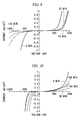
- FIG. 9 shows the results of measuring the leakage current of a dye-sensitized solar cell in which an electrically conductive glass provided with a diffusion-preventing film composed of titanium is used, and based on the results of this graph, the leakage current was confirmed to not increase even when the heat treatment was performed on the electrically conductive glass provided with the diffusion-preventing film composed of titanium. In particular, there was hardly any generation of leakage current at voltages of 500 mV or lower.
- FIG. 10 shows the results of measuring the leakage current of a dye-sensitized solar cell in which an electrically conductive glass provided with a diffusion-preventing film composed of chromium is used, and based on the results of this graph, the leakage current was confirmed to not increase even when the heat treatment was performed on the electrically conductive glass provided with the diffusion-preventing film composed of chromium. In particular, there was hardly any generation of leakage current at voltages of 500 mV or lower.
- FIG. 11 shows the results of measuring the leakage current of a dye-sensitized solar cell in which an electrically conductive film not provided with a diffusion-preventing film is used, and based on the results of this graph, the leakage current was confirmed to increase when the heat treatment was performed after providing a grid composed of nickel.
- the electrically conductive glass of the present invention is provided with a transparent electrically conductive film on a glass surface, and is provided with a grid including a film of a passivated metal on the transparent electrically conductive film, the electrical conductivity of the electrically conductive glass is extremely high, and the thickness of the transparent electrically conductive film can be made to be thin, thereby nearly completely eliminating any blocking of light by the grid to obtain high optical transmittance.
- the grid includes a passivated metal, an insulating, fine oxide film is formed on the surface of the grid enabling the oxide film to function as a barrier, thus, when this glass is incorporated in a dye-sensitized solar cell, a leakage current flowing from the grid towards an electrolyte is inhibited. Thereby, the dye-sensitized solar cell exhibits a high photoelectric conversion efficiency.
- a transparent electrically conductive film is provided on a glass surface
- a diffusion-preventing film is provided on this transparent electrically conductive film
- a grid including a metal film containing nickel is provided on this diffusion-preventing film
- An electrically conductive glass of the present invention can be used for a working electrode of a dye-sensitized solar cell or other photoelectric conversion element, and allows the production of a dye-sensitized solar cell having a high photoelectric conversion efficiency.
Landscapes
- Engineering & Computer Science (AREA)
- Power Engineering (AREA)
- Chemical Kinetics & Catalysis (AREA)
- Electrochemistry (AREA)
- Chemical & Material Sciences (AREA)
- Microelectronics & Electronic Packaging (AREA)
- General Chemical & Material Sciences (AREA)
- Hybrid Cells (AREA)
- Photovoltaic Devices (AREA)
- Non-Insulated Conductors (AREA)
- Glass Compositions (AREA)
- Medicinal Preparation (AREA)
- Medicines Containing Antibodies Or Antigens For Use As Internal Diagnostic Agents (AREA)
- Medicines That Contain Protein Lipid Enzymes And Other Medicines (AREA)
- Surface Treatment Of Glass (AREA)
Abstract
Description
| No. | | Formation Method | |
| 1 | | Vapor deposition | |
| 2 | | Sputtering | |
| 3 | | Plating | |
| 4 | | Plating | |
| 5 | Nickel | Plating | |
| 6 | Gold | Plating | |
| 7 | Platinum | Plating | |
| 8 | Silver | Plating | |
| 9 | Platinum | Plating | Formation of barrier layer composed of titanium oxide |
| 10 | Gold | Plating | Formation of barrier layer composed of |
| 11 | Silver | Plating | Formation of barrier layer composed of |
| 12 | Gold | Plating | Formation of barrier layer composed of |
| 13 | Silver | Plating | Formation of barrier layer composed of FTO |
| Dry Corrosion Resistance | Iodine Resistance | Leakage Current | Dry Corrosion Resistance | Iodine Resistance | Leakage Current | ||
| 1 | C (white dots) | B | A | 8 | B (white dots) | D | - |
| 2 | B (inter- fering color) | B | B | 9 | - | B | C |
| 3 | B (black) | B | B | 10 | - | B | C |
| 4 | B (black) | B | B | 11 | - | B | C |
| 5 | B (black) | B | A | 12 | - | B | D |
| 6 | A | B | D | 13 | - | B | C |
| 7 | A | B | D |
| Ni | Duration of | |||||||
| 5 min. | 10 min. | 30 min. | 60 min. | 90 min. | 120 min. | |||
| Heat treatment temp. | 120°C | D | D | D | | D | C | |
| 150°C | D | C | C | | B | B | ||
| 200°C | C | B | B | B | A | A | ||
| 300°C | B | B | A | A | A | A | ||
| 450°C | A | A | A | A | A | A |
| Cr | Duration of | |||||||
| 5 min. | 10 min. | 30 min. | 60 min. | 90 min. | 120 min. | |||
| Heat treatment temp. | 120°C | D | D | D | | D | C | |
| 150°C | D | D | C | C | C | | ||
| 200°C | D | C | B | B | B | B | ||
| 300°C | B | B | B | B | B | B | ||
| 450°C | B | B | B | B | A | A |
| Co | Duration of | |||||||
| 5 min. | 10 min. | 30 min. | 60 min. | 90 min. | 120 min. | |||
| Heat treatment temp. | 120°C | D | D | D | | D | D | |
| 150°C | D | D | D | | D | D | ||
| 200°C | D | D | D | D | D | C | ||
| 300°C | D | D | C | C | C | B | ||
| 450°C | C | C | B | B | B | B |
| A1 | Duration of | |||||||
| 5 min. | 10 min. | 30 min. | 60 min. | 90 min. | 120 min. | |||
| Heat treatment temp. | 120°C | D | D | D | | D | C | |
| 150°C | C | C | B | | B | B | ||
| 200°C | C | B | B | B | B | B | ||
| 300°C | B | B | B | B | A | A | ||
| 450°C | B | B | A | A | A | A |
| Ti | Duration of | ||||||
| 5 min. | 10 min. | 30 min. | 60 min. | 90 min. | 120 min. | ||
| Heat treatment temp. | 120°C | D | D | D | C | C | C |
| 150°C | D | C | C | | B | B | |
| 200°C | C | B | B | B | B | A | |
| 300°C | B | B | B | A | A | A | |
| 450°C | B | A | A | A | A | A |
Claims (11)
- An electrically conductive glass comprising:a transparent electrically conductive film provided on a glass surface; anda grid comprising a passivated metal film provided on the transparent electrically conductive film.
- An electrically conductive glass according to claim 1,
wherein the passivated metal is nickel, chromium, or cobalt, or an alloy of two or more species thereof. - An electrically conductive glass according to claim 1 or 2,
wherein a thickness of an oxide film formed on the surface of the grid comprising a passivated metal film is 10 to 500 nm. - An electrically conductive glass according to any of claims 1 to 3,
wherein only the surface of the grid is of the passivated metal. - A method of manufacturing an electrically conductive glass, comprising:forming a transparent electrically conductive film on a glass surface; andwhen forming a grid comprising a passivated metal film on the transparent electrically conductive film and obtaining an electrically conductive glass, heat-treating the grid at 120 to 550°C in an oxygen atmosphere.
- An electrically conductive glass comprising:a transparent electrically conductive film provided on a glass surface;a diffusion-preventing film provided on the transparent electrically conductive film; anda grid comprising a metal film containing nickel provided on the diffusion-preventing film.
- An electrically conductive glass comprising:a transparent electrically conductive film provided on a glass surface;a grid comprising a metal film containing nickel provided on the transparent electrically conductive film; anda diffusion-preventing film provided on the grid and on the transparent electrically conductive film.
- An electrically conductive glass according to claim 6 or 7,
wherein the diffusion-preventing film is formed from titanium, titanium oxide, niobium, or chromium. - An electrically conductive glass according to claim 8,
wherein a thickness of the titanium oxide that forms the diffusion-preventing film is 0.1 µm or less. - A photoelectric conversion element
wherein the electrically conductive glass according to any of claims 1, 2, 3, 4, 6, 7, 8, or 9 is used. - A photoelectric conversion element according to claim 10,
which is a dye-sensitized solar cell.
Applications Claiming Priority (5)
| Application Number | Priority Date | Filing Date | Title |
|---|---|---|---|
| JP2002086859 | 2002-03-26 | ||
| JP2002086859 | 2002-03-26 | ||
| JP2002333598 | 2002-11-18 | ||
| JP2002333598 | 2002-11-18 | ||
| PCT/JP2003/003626 WO2003081609A1 (en) | 2002-03-26 | 2003-03-25 | Conductive glass and photoelectric conversion device using same |
Publications (3)
| Publication Number | Publication Date |
|---|---|
| EP1489628A1 true EP1489628A1 (en) | 2004-12-22 |
| EP1489628A4 EP1489628A4 (en) | 2008-01-02 |
| EP1489628B1 EP1489628B1 (en) | 2010-12-01 |
Family
ID=28456269
Family Applications (1)
| Application Number | Title | Priority Date | Filing Date |
|---|---|---|---|
| EP03720892A Expired - Lifetime EP1489628B1 (en) | 2002-03-26 | 2003-03-25 | Conductive glass for photoelectric conversion device |
Country Status (10)
| Country | Link |
|---|---|
| US (1) | US8546683B2 (en) |
| EP (1) | EP1489628B1 (en) |
| JP (1) | JP4071719B2 (en) |
| KR (1) | KR100612458B1 (en) |
| CN (1) | CN1326158C (en) |
| AT (1) | ATE490542T1 (en) |
| AU (1) | AU2003236063B2 (en) |
| DE (1) | DE60335179D1 (en) |
| TW (1) | TWI234885B (en) |
| WO (1) | WO2003081609A1 (en) |
Cited By (5)
| Publication number | Priority date | Publication date | Assignee | Title |
|---|---|---|---|---|
| EP1521328A4 (en) * | 2002-07-09 | 2010-05-12 | Fujikura Ltd | SOLAR CELL |
| US7825330B2 (en) * | 2002-07-09 | 2010-11-02 | Fujikura Ltd. | Solar cell |
| US8470150B2 (en) | 2010-09-08 | 2013-06-25 | Industrial Technology Research Institute | Method of fabricating electrode structures on substrate |
| EP2418665A3 (en) * | 2010-08-11 | 2013-08-21 | Samsung SDI Co., Ltd. | Electrode for photoelectric device, method of preparing the same and photoelectric device comprising the same |
| US9139465B2 (en) | 2009-08-04 | 2015-09-22 | Lehigh University | Conductive doped metal-glass compositions and methods |
Families Citing this family (47)
| Publication number | Priority date | Publication date | Assignee | Title |
|---|---|---|---|---|
| WO2008139479A2 (en) * | 2007-05-15 | 2008-11-20 | 3Gsolar Ltd. | Photovoltaic cell |
| IL153895A (en) * | 2003-01-12 | 2013-01-31 | Orion Solar Systems Ltd | Solar cell device |
| JP4578786B2 (en) * | 2003-07-23 | 2010-11-10 | 株式会社フジクラ | Method for producing dye-sensitized solar cell |
| JP4797324B2 (en) * | 2004-01-09 | 2011-10-19 | 株式会社ブリヂストン | Dye-sensitized solar cell electrode |
| JP4892197B2 (en) * | 2005-04-01 | 2012-03-07 | 関西パイプ工業株式会社 | Electrode substrate for dye-sensitized solar cell, photoelectrode and counter electrode for dye-sensitized solar cell, and dye-sensitized solar cell |
| JP2006294423A (en) * | 2005-04-11 | 2006-10-26 | Ngk Spark Plug Co Ltd | Dye-sensitized solar cell |
| JP4966525B2 (en) * | 2005-08-10 | 2012-07-04 | 株式会社エンプラス | Dye-sensitized solar cell, its photoelectrode substrate, and method for producing the photoelectrode substrate |
| FR2895206B1 (en) * | 2005-12-16 | 2008-03-21 | Framatome Anp Sas | HEATED ROD FOR PRIMARY CIRCUIT PRESSURIZER OF A PRESSURE WATER NUCLEAR REACTOR. |
| US8754323B2 (en) * | 2006-06-29 | 2014-06-17 | National University Corporation Kyushu Institute Of Technology | Dye-sensitized solar cell and process for producing the same |
| KR100811007B1 (en) * | 2006-08-25 | 2008-03-11 | 주식회사 신안에스엔피 | Method for manufacturing solar cell using ITO transparent conductive thin film and liquid crystal display device with solar cell manufactured by the method |
| EP2092573A2 (en) | 2006-11-01 | 2009-08-26 | Bar-Ilan University | Nickel-cobalt alloys as current collectors and conductive interconnects and deposition thereof on transparent conductive oxides |
| JP5141685B2 (en) * | 2007-06-11 | 2013-02-13 | コニカミノルタホールディングス株式会社 | Method for manufacturing photoelectric conversion element |
| JP5096064B2 (en) * | 2007-08-01 | 2012-12-12 | シャープ株式会社 | Dye-sensitized solar cell module |
| JP5252929B2 (en) * | 2008-01-16 | 2013-07-31 | ラピスセミコンダクタ株式会社 | Dye-sensitized solar cell and method for producing the same |
| US7833808B2 (en) * | 2008-03-24 | 2010-11-16 | Palo Alto Research Center Incorporated | Methods for forming multiple-layer electrode structures for silicon photovoltaic cells |
| WO2009157177A1 (en) * | 2008-06-24 | 2009-12-30 | 日本曹達株式会社 | Transparent conductive film having fto/ito multilayer body |
| JP5273709B2 (en) * | 2008-07-02 | 2013-08-28 | シャープ株式会社 | Dye-sensitized solar cell, method for producing the same, and dye-sensitized solar cell module |
| WO2010077622A1 (en) * | 2008-12-08 | 2010-07-08 | Arizona Board Of Regents, Acting For And On Behalf Of Arizona State University | Electrical devices including dendritic metal electrodes |
| WO2010107795A1 (en) * | 2009-03-17 | 2010-09-23 | Konarka Technologies, Inc. | Metal substrate for a dye sensitized photovoltaic cell |
| EP2259329A1 (en) * | 2009-05-26 | 2010-12-08 | Institut de Ciències Fotòniques, Fundació Privada | Metal transparent conductors with low sheet resistance |
| EP2309547B1 (en) * | 2009-10-06 | 2012-12-12 | Samsung SDI Co., Ltd. | Photoelectric conversion device |
| EP2312641A1 (en) * | 2009-10-13 | 2011-04-20 | Ecole Polytechnique Fédérale de Lausanne (EPFL) | Device comprising electrical contacts and its production process |
| US20110168253A1 (en) * | 2009-12-25 | 2011-07-14 | Samsung Sdi Co., Ltd. | Electrode substrate and photoelectric transformation device |
| ES2364309B1 (en) * | 2010-02-19 | 2012-08-13 | Institut De Ciencies Fotoniques, Fundacio Privada | TRANSPARENT ELECTRODE BASED ON THE COMBINATION OF OXIDES, METALS AND TRANSPARENT DRIVING OXIDES. |
| US20110214730A1 (en) * | 2010-03-04 | 2011-09-08 | Casio Computer Co., Ltd. | Dye-sensitized solar cell |
| CN102194898B (en) * | 2010-03-15 | 2013-03-27 | 常州天合光能有限公司 | Electric-conducting nickel paste for solar cell |
| CN103081085A (en) * | 2010-08-06 | 2013-05-01 | 旭硝子株式会社 | Support substrate |
| WO2012029755A2 (en) * | 2010-09-01 | 2012-03-08 | 東洋紡績株式会社 | Light-diffusing laminated film |
| US9356172B2 (en) | 2010-09-16 | 2016-05-31 | Lg Innotek Co., Ltd. | Solar cell and method for manufacturing same |
| KR101091375B1 (en) * | 2010-09-16 | 2011-12-07 | 엘지이노텍 주식회사 | Solar cell and manufacturing method thereof |
| CN101964398A (en) * | 2010-10-11 | 2011-02-02 | 福建钧石能源有限公司 | Flexible thin film solar cell and manufacturing method thereof |
| JP5760003B2 (en) * | 2010-10-29 | 2015-08-05 | リンテック株式会社 | Transparent conductive film, electronic device, and method for manufacturing electronic device |
| KR101628393B1 (en) * | 2010-11-05 | 2016-06-22 | 현대자동차주식회사 | Method for manufacturing conductive substrate for an electrode of photovoltaics |
| US20130008687A1 (en) * | 2011-07-08 | 2013-01-10 | Industrial Technology Research Institute | Conductive film structure capable of resisting moisture and oxygen and electronic apparatus using the same |
| US8529747B2 (en) * | 2011-07-12 | 2013-09-10 | The Boeing Company | Methods for repairing steel components |
| WO2013073045A1 (en) * | 2011-11-18 | 2013-05-23 | 三洋電機株式会社 | Solar cell and production method for solar cell |
| US9805841B2 (en) * | 2012-07-03 | 2017-10-31 | Massachusetts Institute Of Technology | Virus film as template for porous inorganic scaffolds |
| CN102800752A (en) * | 2012-08-16 | 2012-11-28 | 青海天普太阳能科技有限公司 | Method for preparing diffusion barrier layer of flexible silicon-based solar cell |
| CN103187119B (en) | 2013-02-06 | 2014-08-06 | 南昌欧菲光科技有限公司 | Conductive film, preparation method for conductive film and touch screen comprising conductive film |
| US10840400B2 (en) * | 2013-08-29 | 2020-11-17 | Taiwan Semiconductor Manufacturing Co., Ltd. | Photovoltaic device with back reflector |
| KR20150031917A (en) * | 2013-09-17 | 2015-03-25 | 엘지이노텍 주식회사 | Electrode Plate and Eletrochomic Plate, Electrochomic Mirror and Display Device Using the Same |
| US20150228374A1 (en) * | 2014-02-07 | 2015-08-13 | E I Du Pont De Nemours And Company | Thermally conductive electronic substrates and methods relating thereto |
| JP6310312B2 (en) * | 2014-04-18 | 2018-04-11 | キヤノン株式会社 | Photoelectric conversion element and manufacturing method thereof |
| JP6832658B2 (en) * | 2016-09-23 | 2021-02-24 | スタンレー電気株式会社 | Light transmission board, display device, signal device, and lighting device |
| WO2019165234A1 (en) * | 2018-02-23 | 2019-08-29 | Ohio State Innovation Foundation | Passivated conductive films, and electroactuators containing same |
| CN111129189B (en) * | 2019-12-11 | 2022-04-12 | 中国电子科技集团公司第十八研究所 | A kind of ITO glass cover sheet for space and preparation method thereof |
| JP2024178538A (en) * | 2023-06-13 | 2024-12-25 | 三星電子株式会社 | Transparent electrodes and measuring devices |
Family Cites Families (12)
| Publication number | Priority date | Publication date | Assignee | Title |
|---|---|---|---|---|
| JPS6012604A (en) * | 1983-06-30 | 1985-01-23 | 日東電工株式会社 | Composite material with transparent conductive film |
| JPS60262304A (en) * | 1984-06-07 | 1985-12-25 | 旭硝子株式会社 | Conductor |
| JPS61116883A (en) * | 1984-11-13 | 1986-06-04 | Toa Nenryo Kogyo Kk | Transparent electrode with metal wiring |
| JPS62127586U (en) * | 1986-02-03 | 1987-08-13 | ||
| JP2710318B2 (en) * | 1987-11-26 | 1998-02-10 | 株式会社デンソー | Translucent solar cell |
| JPH0733301Y2 (en) * | 1989-12-26 | 1995-07-31 | 三洋電機株式会社 | Photoelectric conversion device |
| JPH1056190A (en) * | 1996-08-08 | 1998-02-24 | Canon Inc | Photovoltaic element and method for manufacturing the same |
| US6291763B1 (en) * | 1999-04-06 | 2001-09-18 | Fuji Photo Film Co., Ltd. | Photoelectric conversion device and photo cell |
| US6580026B1 (en) * | 1999-06-30 | 2003-06-17 | Catalysts & Chemicals Industries Co., Ltd. | Photovoltaic cell |
| WO2001048833A1 (en) * | 1999-12-27 | 2001-07-05 | Seiko Epson Corporation | Solar cell and solar cell unit |
| JP4461656B2 (en) * | 2000-12-07 | 2010-05-12 | セイコーエプソン株式会社 | Photoelectric conversion element |
| JP2003203681A (en) | 2001-12-28 | 2003-07-18 | Fujikura Ltd | Conductive glass for photoelectric conversion elements |
-
2003
- 2003-03-21 TW TW092106381A patent/TWI234885B/en not_active IP Right Cessation
- 2003-03-25 DE DE60335179T patent/DE60335179D1/en not_active Expired - Lifetime
- 2003-03-25 CN CNB038069466A patent/CN1326158C/en not_active Expired - Lifetime
- 2003-03-25 AT AT03720892T patent/ATE490542T1/en active
- 2003-03-25 AU AU2003236063A patent/AU2003236063B2/en not_active Ceased
- 2003-03-25 JP JP2003579235A patent/JP4071719B2/en not_active Expired - Fee Related
- 2003-03-25 WO PCT/JP2003/003626 patent/WO2003081609A1/en not_active Ceased
- 2003-03-25 KR KR1020047015140A patent/KR100612458B1/en not_active Expired - Fee Related
- 2003-03-25 EP EP03720892A patent/EP1489628B1/en not_active Expired - Lifetime
-
2004
- 2004-09-23 US US10/947,225 patent/US8546683B2/en not_active Expired - Fee Related
Cited By (6)
| Publication number | Priority date | Publication date | Assignee | Title |
|---|---|---|---|---|
| EP1521328A4 (en) * | 2002-07-09 | 2010-05-12 | Fujikura Ltd | SOLAR CELL |
| US7825330B2 (en) * | 2002-07-09 | 2010-11-02 | Fujikura Ltd. | Solar cell |
| US9139465B2 (en) | 2009-08-04 | 2015-09-22 | Lehigh University | Conductive doped metal-glass compositions and methods |
| US9403712B2 (en) | 2009-08-04 | 2016-08-02 | Lehigh University | Conductive doped metal-glass compositions and methods |
| EP2418665A3 (en) * | 2010-08-11 | 2013-08-21 | Samsung SDI Co., Ltd. | Electrode for photoelectric device, method of preparing the same and photoelectric device comprising the same |
| US8470150B2 (en) | 2010-09-08 | 2013-06-25 | Industrial Technology Research Institute | Method of fabricating electrode structures on substrate |
Also Published As
| Publication number | Publication date |
|---|---|
| CN1326158C (en) | 2007-07-11 |
| TW200306014A (en) | 2003-11-01 |
| US8546683B2 (en) | 2013-10-01 |
| WO2003081609A1 (en) | 2003-10-02 |
| JP4071719B2 (en) | 2008-04-02 |
| EP1489628B1 (en) | 2010-12-01 |
| TWI234885B (en) | 2005-06-21 |
| DE60335179D1 (en) | 2011-01-13 |
| US20050034755A1 (en) | 2005-02-17 |
| JPWO2003081609A1 (en) | 2005-07-28 |
| KR100612458B1 (en) | 2006-08-16 |
| AU2003236063B2 (en) | 2006-04-06 |
| AU2003236063A1 (en) | 2003-10-08 |
| ATE490542T1 (en) | 2010-12-15 |
| EP1489628A4 (en) | 2008-01-02 |
| KR20040095320A (en) | 2004-11-12 |
| CN1643621A (en) | 2005-07-20 |
Similar Documents
| Publication | Publication Date | Title |
|---|---|---|
| US8546683B2 (en) | Electrically conductive glass and photoelectric conversion element using the same | |
| AU2007252623B2 (en) | Method of manufacturing electrode substrate, electrode substrate, photoelectric conversion element, and dye-sensitized solar cell | |
| TWI326920B (en) | Electrode substrate, photoelectric transducer, conductive glass substrate and manufacturing method thereof, and dye-sensitized solar cell | |
| JP4503226B2 (en) | Electrode substrate, photoelectric conversion element, and dye-sensitized solar cell | |
| JP5367817B2 (en) | Wet solar cell module | |
| JP2004128267A (en) | Conductive glass substrate for photoelectric conversion element and method for producing the same | |
| AU2006276649C1 (en) | Electrode substrate and photoelectric converter | |
| KR20100075552A (en) | Dye-sensitized solar cell module | |
| JP4578786B2 (en) | Method for producing dye-sensitized solar cell | |
| JP4203554B2 (en) | Photoelectric conversion element and manufacturing method thereof | |
| JP2003203683A (en) | Conductive glass for photoelectric conversion elements | |
| JP2014031583A (en) | Nickel-cobalt alloys as current collectors and conductive wiring, and deposition thereof on transparent conductive oxides | |
| JP3441361B2 (en) | Photoelectric conversion element | |
| JP2003203681A (en) | Conductive glass for photoelectric conversion elements | |
| JP4416997B2 (en) | Electrode substrate for dye-sensitized solar cell, photoelectric conversion element, and dye-sensitized solar cell | |
| JP2004039471A (en) | Dye-sensitized solar cell | |
| JP2003203682A (en) | Conductive glass for photoelectric conversion elements | |
| JP4954855B2 (en) | Manufacturing method of dye-sensitized solar cell | |
| JP2005285473A (en) | Photoelectric conversion device | |
| KR100908243B1 (en) | Dye-Sensitized Solar Cell Including Electron Recombination Blocking Layer and Manufacturing Method Thereof | |
| Ivanou et al. | Embedded chromium current collectors for efficient and stable large area dye sensitized solar cells | |
| KR20070072215A (en) | Electrode for photoelectric conversion element having a metal mesh layer, a manufacturing method thereof and a dye-sensitized solar cell employing the electrode | |
| JP2003123855A (en) | Photoelectrode for photoelectric conversion element | |
| JP2006147411A (en) | Electrode, photoelectric conversion element, and dye-sensitized solar cell | |
| JP2006083036A (en) | Etching method of glass, manufacturing method of transparent conductive substrate, and photoelectric conversion element |
Legal Events
| Date | Code | Title | Description |
|---|---|---|---|
| PUAI | Public reference made under article 153(3) epc to a published international application that has entered the european phase |
Free format text: ORIGINAL CODE: 0009012 |
|
| 17P | Request for examination filed |
Effective date: 20040923 |
|
| AK | Designated contracting states |
Kind code of ref document: A1 Designated state(s): AT BE BG CH CY CZ DE DK EE ES FI FR GB GR HU IE IT LI LU MC NL PT RO SE SI SK TR |
|
| AX | Request for extension of the european patent |
Extension state: AL LT LV MK |
|
| A4 | Supplementary search report drawn up and despatched |
Effective date: 20071204 |
|
| 17Q | First examination report despatched |
Effective date: 20080313 |
|
| GRAP | Despatch of communication of intention to grant a patent |
Free format text: ORIGINAL CODE: EPIDOSNIGR1 |
|
| RIC1 | Information provided on ipc code assigned before grant |
Ipc: H01L 31/04 20060101ALI20100802BHEP Ipc: H01M 14/00 20060101ALI20100802BHEP Ipc: H01B 5/14 20060101ALI20100802BHEP Ipc: H01G 9/20 20060101AFI20100802BHEP Ipc: B32B 17/06 20060101ALI20100802BHEP |
|
| RTI1 | Title (correction) |
Free format text: CONDUCTIVE GLASS FOR PHOTOELECTRIC CONVERSION DEVICE |
|
| GRAS | Grant fee paid |
Free format text: ORIGINAL CODE: EPIDOSNIGR3 |
|
| RIN1 | Information on inventor provided before grant (corrected) |
Inventor name: MATSUI, HIROSHI,FUJIKURA LTD. Inventor name: OKADA, KENICHI,FUJIKURA LTD. Inventor name: TANABE, NOBUO,FUJIKURA LTD. |
|
| GRAA | (expected) grant |
Free format text: ORIGINAL CODE: 0009210 |
|
| AK | Designated contracting states |
Kind code of ref document: B1 Designated state(s): AT CH DE FI LI NL SE |
|
| REG | Reference to a national code |
Ref country code: CH Ref legal event code: EP |
|
| REF | Corresponds to: |
Ref document number: 60335179 Country of ref document: DE Date of ref document: 20110113 Kind code of ref document: P |
|
| REG | Reference to a national code |
Ref country code: SE Ref legal event code: TRGR |
|
| REG | Reference to a national code |
Ref country code: CH Ref legal event code: NV Representative=s name: SCHMAUDER & PARTNER AG PATENT- UND MARKENANWAELTE |
|
| REG | Reference to a national code |
Ref country code: NL Ref legal event code: T3 |
|
| PGFP | Annual fee paid to national office [announced via postgrant information from national office to epo] |
Ref country code: FI Payment date: 20110328 Year of fee payment: 9 Ref country code: SE Payment date: 20110325 Year of fee payment: 9 |
|
| PGFP | Annual fee paid to national office [announced via postgrant information from national office to epo] |
Ref country code: CH Payment date: 20110405 Year of fee payment: 9 |
|
| PLBE | No opposition filed within time limit |
Free format text: ORIGINAL CODE: 0009261 |
|
| STAA | Information on the status of an ep patent application or granted ep patent |
Free format text: STATUS: NO OPPOSITION FILED WITHIN TIME LIMIT |
|
| 26N | No opposition filed |
Effective date: 20110902 |
|
| REG | Reference to a national code |
Ref country code: DE Ref legal event code: R097 Ref document number: 60335179 Country of ref document: DE Effective date: 20110902 |
|
| PGFP | Annual fee paid to national office [announced via postgrant information from national office to epo] |
Ref country code: NL Payment date: 20120322 Year of fee payment: 10 |
|
| REG | Reference to a national code |
Ref country code: SE Ref legal event code: EUG |
|
| PG25 | Lapsed in a contracting state [announced via postgrant information from national office to epo] |
Ref country code: FI Free format text: LAPSE BECAUSE OF NON-PAYMENT OF DUE FEES Effective date: 20120325 Ref country code: SE Free format text: LAPSE BECAUSE OF NON-PAYMENT OF DUE FEES Effective date: 20120326 |
|
| REG | Reference to a national code |
Ref country code: CH Ref legal event code: PL |
|
| PG25 | Lapsed in a contracting state [announced via postgrant information from national office to epo] |
Ref country code: LI Free format text: LAPSE BECAUSE OF NON-PAYMENT OF DUE FEES Effective date: 20120331 Ref country code: CH Free format text: LAPSE BECAUSE OF NON-PAYMENT OF DUE FEES Effective date: 20120331 |
|
| PGFP | Annual fee paid to national office [announced via postgrant information from national office to epo] |
Ref country code: AT Payment date: 20120228 Year of fee payment: 10 |
|
| REG | Reference to a national code |
Ref country code: NL Ref legal event code: V1 Effective date: 20131001 |
|
| REG | Reference to a national code |
Ref country code: AT Ref legal event code: MM01 Ref document number: 490542 Country of ref document: AT Kind code of ref document: T Effective date: 20130325 |
|
| PG25 | Lapsed in a contracting state [announced via postgrant information from national office to epo] |
Ref country code: AT Free format text: LAPSE BECAUSE OF NON-PAYMENT OF DUE FEES Effective date: 20130325 |
|
| PG25 | Lapsed in a contracting state [announced via postgrant information from national office to epo] |
Ref country code: NL Free format text: LAPSE BECAUSE OF NON-PAYMENT OF DUE FEES Effective date: 20131001 |
|
| PGFP | Annual fee paid to national office [announced via postgrant information from national office to epo] |
Ref country code: DE Payment date: 20180313 Year of fee payment: 16 |
|
| REG | Reference to a national code |
Ref country code: DE Ref legal event code: R119 Ref document number: 60335179 Country of ref document: DE |
|
| PG25 | Lapsed in a contracting state [announced via postgrant information from national office to epo] |
Ref country code: DE Free format text: LAPSE BECAUSE OF NON-PAYMENT OF DUE FEES Effective date: 20191001 |