EP1484791A1 - Dicing method, method of inspecting integrated circuit element, substrate holding device, and pressure sensitive adhesive film - Google Patents
Dicing method, method of inspecting integrated circuit element, substrate holding device, and pressure sensitive adhesive film Download PDFInfo
- Publication number
- EP1484791A1 EP1484791A1 EP03743517A EP03743517A EP1484791A1 EP 1484791 A1 EP1484791 A1 EP 1484791A1 EP 03743517 A EP03743517 A EP 03743517A EP 03743517 A EP03743517 A EP 03743517A EP 1484791 A1 EP1484791 A1 EP 1484791A1
- Authority
- EP
- European Patent Office
- Prior art keywords
- adhesive film
- integrated circuit
- semiconductor substrate
- adhesion
- circuit elements
- Prior art date
- Legal status (The legal status is an assumption and is not a legal conclusion. Google has not performed a legal analysis and makes no representation as to the accuracy of the status listed.)
- Withdrawn
Links
Images




Classifications
-
- H—ELECTRICITY
- H10—SEMICONDUCTOR DEVICES; ELECTRIC SOLID-STATE DEVICES NOT OTHERWISE PROVIDED FOR
- H10P—GENERIC PROCESSES OR APPARATUS FOR THE MANUFACTURE OR TREATMENT OF DEVICES COVERED BY CLASS H10
- H10P95/00—Generic processes or apparatus for manufacture or treatments not covered by the other groups of this subclass
-
- H—ELECTRICITY
- H10—SEMICONDUCTOR DEVICES; ELECTRIC SOLID-STATE DEVICES NOT OTHERWISE PROVIDED FOR
- H10P—GENERIC PROCESSES OR APPARATUS FOR THE MANUFACTURE OR TREATMENT OF DEVICES COVERED BY CLASS H10
- H10P72/00—Handling or holding of wafers, substrates or devices during manufacture or treatment thereof
- H10P72/04—Apparatus for manufacture or treatment
- H10P72/0442—Apparatus for placing on an insulating substrate, e.g. tape
-
- B—PERFORMING OPERATIONS; TRANSPORTING
- B28—WORKING CEMENT, CLAY, OR STONE
- B28D—WORKING STONE OR STONE-LIKE MATERIALS
- B28D5/00—Fine working of gems, jewels, crystals, e.g. of semiconductor material; apparatus or devices therefor
- B28D5/0058—Accessories specially adapted for use with machines for fine working of gems, jewels, crystals, e.g. of semiconductor material
- B28D5/0082—Accessories specially adapted for use with machines for fine working of gems, jewels, crystals, e.g. of semiconductor material for supporting, holding, feeding, conveying or discharging work
-
- H—ELECTRICITY
- H10—SEMICONDUCTOR DEVICES; ELECTRIC SOLID-STATE DEVICES NOT OTHERWISE PROVIDED FOR
- H10P—GENERIC PROCESSES OR APPARATUS FOR THE MANUFACTURE OR TREATMENT OF DEVICES COVERED BY CLASS H10
- H10P72/00—Handling or holding of wafers, substrates or devices during manufacture or treatment thereof
- H10P72/70—Handling or holding of wafers, substrates or devices during manufacture or treatment thereof for supporting or gripping
- H10P72/74—Handling or holding of wafers, substrates or devices during manufacture or treatment thereof for supporting or gripping using temporarily an auxiliary support
-
- H—ELECTRICITY
- H10—SEMICONDUCTOR DEVICES; ELECTRIC SOLID-STATE DEVICES NOT OTHERWISE PROVIDED FOR
- H10P—GENERIC PROCESSES OR APPARATUS FOR THE MANUFACTURE OR TREATMENT OF DEVICES COVERED BY CLASS H10
- H10P72/00—Handling or holding of wafers, substrates or devices during manufacture or treatment thereof
- H10P72/70—Handling or holding of wafers, substrates or devices during manufacture or treatment thereof for supporting or gripping
- H10P72/74—Handling or holding of wafers, substrates or devices during manufacture or treatment thereof for supporting or gripping using temporarily an auxiliary support
- H10P72/7402—Wafer tapes, e.g. grinding or dicing support tapes
-
- H—ELECTRICITY
- H10—SEMICONDUCTOR DEVICES; ELECTRIC SOLID-STATE DEVICES NOT OTHERWISE PROVIDED FOR
- H10P—GENERIC PROCESSES OR APPARATUS FOR THE MANUFACTURE OR TREATMENT OF DEVICES COVERED BY CLASS H10
- H10P72/00—Handling or holding of wafers, substrates or devices during manufacture or treatment thereof
- H10P72/70—Handling or holding of wafers, substrates or devices during manufacture or treatment thereof for supporting or gripping
- H10P72/74—Handling or holding of wafers, substrates or devices during manufacture or treatment thereof for supporting or gripping using temporarily an auxiliary support
- H10P72/7412—Handling or holding of wafers, substrates or devices during manufacture or treatment thereof for supporting or gripping using temporarily an auxiliary support the auxiliary support including means facilitating the separation of a device or wafer from the auxiliary support
- H10P72/7414—Handling or holding of wafers, substrates or devices during manufacture or treatment thereof for supporting or gripping using temporarily an auxiliary support the auxiliary support including means facilitating the separation of a device or wafer from the auxiliary support the auxiliary support including means facilitating the selective separation of some of a plurality of devices from the auxiliary support
-
- H—ELECTRICITY
- H10—SEMICONDUCTOR DEVICES; ELECTRIC SOLID-STATE DEVICES NOT OTHERWISE PROVIDED FOR
- H10P—GENERIC PROCESSES OR APPARATUS FOR THE MANUFACTURE OR TREATMENT OF DEVICES COVERED BY CLASS H10
- H10P72/00—Handling or holding of wafers, substrates or devices during manufacture or treatment thereof
- H10P72/70—Handling or holding of wafers, substrates or devices during manufacture or treatment thereof for supporting or gripping
- H10P72/74—Handling or holding of wafers, substrates or devices during manufacture or treatment thereof for supporting or gripping using temporarily an auxiliary support
- H10P72/7416—Handling or holding of wafers, substrates or devices during manufacture or treatment thereof for supporting or gripping using temporarily an auxiliary support used during dicing or grinding
Definitions
- the present invention relates to a method of dicing a semiconductor substrate on which a plurality of integrated circuit elements are arranged in a matrix, a method of testing the electrical characteristics of the diced integrated circuit elements, a substrate holding apparatus usable in these methods, and an adhesive film usable in the substrate holding apparatus.
- a number of integrated circuit elements are arranged in a matrix on a semiconductor wafer (referred to as a "wafer” hereinafter) subjected to a series of fabrication processes. These elements are separated into individual elements by a conventional dicing method as shown in FIG. 13. That is, a holder 10 obtained by adhering an adhesive layer (e.g., an adhesive film 12 (e.g., 100 to 200 ⁇ m) having an adhesive upper surface 12a) to one surface of a ring-like frame 11 larger than the size of a wafer W is used. The holder 10 having the wafer W adhered to the adhesive surface 12a of the adhesive film 12 is placed on a chuck table 13.
- an adhesive layer e.g., an adhesive film 12 (e.g., 100 to 200 ⁇ m) having an adhesive upper surface 12a
- the holder 10 having the wafer W adhered to the adhesive surface 12a of the adhesive film 12 is placed on a chuck table 13.
- elements C are separated (for the sake of convenience, the integrated circuit elements and chips are denoted by the same reference symbol "C").
- the holder 10 is unloaded from the chuck table 13.
- the chips C are peeled one by one from the adhesive film 12 as they are pushed up from the lower surface of the adhesive film by a pushing means.
- a handling apparatus transports the peeled chips to the next step.
- the chips C are loaded one by one into a testing apparatus by the handling apparatus, and tested.
- the handling apparatus easily causes trouble when handling small chips of about 1.5 mm square.
- the present invention has been developed under the circumstances described above.
- the present invention provides a dicing method and testing method capable of increasing the efficiency of testing of integrated circuit chips, and a substrate holding apparatus and adhesive film usable in these methods.
- a dicing method of a semiconductor substrate on which a plurality of integrated circuit elements are arranged in a matrix comprises: adhering at least an entire region on the rear surface of the semiconductor substrate, which opposed a surface on which the integrated circuit elements are arranged, to a plate-like jig via at least one adhesive layer having adhesion properties (the adhesion of the adhesive layer is reduced when energy is applied to the adhesive layer); and separating the integrated circuit elements by cutting the semiconductor substrate by cutting means.
- a testing method of a plurality of integrated circuit chips formed on a semiconductor substrate comprises: adhering the rear surface of the semiconductor substrate, which opposed a surface on which the plurality of integrated circuit chips are formed, on a plate-like jig by at least one adhesive layer formed over at least an entire region in which the integrated circuit elements are arranged; cutting the semiconductor substrate by cutting means to separate the plurality of integrated circuit elements into individual integrated circuit elements (the cut semiconductor substrate is adhered on the jig by the adhesive layer); aligning the semiconductor substrate adhered on the jig with a probe positioned in a space above the jig; and testing the electrical characteristics of the integrated circuit elements while the probe is in contact with electrode pads of the integrated circuit elements.
- a substrate holding apparatus for holding a semiconductor substrate on which a plurality of integrated circuit elements are arranged.
- This substrate holding apparatus comprises: a frame having a size larger than the semiconductor substrate; an adhesive film stretched on the frame, one surface of the adhesive film being a surface to which the rear surface of the semiconductor substrate is adhered; and a plate-like jig (the other surface of the adhesive film is adhered to the jig).
- Each of the semiconductor substrate dicing method, integrated circuit chip testing method, and substrate holding apparatus provided in accordance with the first, second, and third aspects of the present application preferably comprises one of items (1) to (12) below, and more preferably comprises a combination of a plurality of items of (1) to (12).
- This embodiment includes embodiments of a dicing method, substrate holding apparatus, and adhesive tape for integrated circuit elements of the present invention.
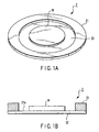
- a substrate holding apparatus (to be referred to as a "holder” hereinafter) used in this embodiment will be described below with reference to FIGS. 1A and 1B.
- a holder 2 comprises a frame (e.g., a ring-like frame) 21 larger than the size of a wafer, and a first adhesive layer (e.g., a first adhesive film) 22 stretched on the frame 21.
- This adhesive film can have the same size as the outer circumference of the frame.
- the adhesion of one surface (first surface) 22a of the first adhesive film 22 is reduced by the application of energy (e.g., ultraviolet radiation). This surface is adhered to one surface of the frame 21 and stretched inside the frame 21.
- energy e.g., ultraviolet radiation
- a semiconductor substrate e.g., a silicon substrate (to be referred to as a "wafer W" hereinafter) on which a number of integrated circuit elements are arranged in a matrix is adhered to a central portion of the holder 2 (strictly speaking, a central portion of the first adhesive film 22).
- a handling apparatus can transport the wafer W by holding the frame 21 of the holder 2.
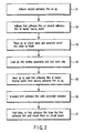
- FIG. 2 is a flowchart showing the entire flow of a testing method according to this embodiment.
- a fourth surface 4b of adhesive layers e.g., a second adhesive film having adhesion properties
- a plate-like jig 3 e.g., a circular plate having a thickness of about 1 mm and substantially the same size as the outer diameter of the frame 21
- the adhesion of the second adhesive film 4 is reduced by the application of energy (e.g., heat).
- the material of the jig 3 it is preferable to use a material whose thermal expansion is close to or smaller than the thermal expansion of a silicon wafer.
- Invar aluminum nitride
- SiC silicon carbide
- the reason is to reduce positional shift between chips caused by thermal expansion of the chips when they are heated during testing.
- a second surface 22b of the first adhesive film 22 stretched on the holder 2 having the wafer W is adhered to a third surface 4a of the second adhesive film 4 on the jig 3 (step S2).
- the first adhesive film 22 and second. adhesive film 4 form an adhesive layer for adhering the wafer W to the jig 3, and the thickness of each film is, e.g., 100 to 200 ⁇ m.
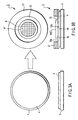
- the jig 3 having the wafer W is placed on a chuck table 5.
- the jig 3 is fixed to the chuck table 5 by suction by a vacuum drawing force which a suction pump 84 forms in suction holes 81 via a suction pipe 83.
- a rotating blade 51 as a cutting means moves along scribe lines 52' on the wafer W, and cuts the wafer W from cut lines 52.
- a plurality of integrated circuit chips C are separated into individual chips. While the blade 51 is cutting the wafer W, water can be supplied to the cut portion by a water supply means 50 or the like.
- the cut lines 52 may also extend to half the thickness the first adhesive film 22.
- the chuck table 5 can move in the X, Y, and Z directions, and can rotate around a vertical axis. After the blade 51 and wafer W are aligned, dicing can be performed by accurately moving the chuck table 5 relative to the rotating blade 51 (step S3). It is also possible to move the rotating blade 51 relative to the chuck table 5. Furthermore, another means such as a laser cutting means may also be used as the cutting means.
- FIG. 5 is a view showing the holder 2 having the diced wafer from above.
- the jig 3 is loaded into a testing apparatus (e.g., a prober), and placed on a chuck table 6 as shown in FIG. 6.
- the jig 3 is fixed to the chuck table 6 by suction from suction holes 81.
- probes e.g., probe needles 61 formed on a probe card 60 are brought into contact with electrode pads of the chips C.
- a tester 62 tests the electrical characteristics of each chip C. For example, it is possible to collectively bring the probe needles 61 into contact with a plurality of electrode pads of a plurality of chips C, and simultaneously test the electrical characteristics of the plurality of chips C (step S4).
- the tester 62 can apply a testing pulse to a plurality of chips C in turn.
- "Simultaneously test the electrical characteristics of a plurality of chips C” means that a plurality of probe needles 61 simultaneously come in contact with a plurality of electrode pads of a plurality of chips C. Therefore, a micro timing delay between the timings at which the testing pulse is applied to the probes 61 in turn is not a problem.
- the chuck table 6 can move in the X, Y, and Z directions, and can rotate around a vertical axis. After the wafer W (the wafer W herein mentioned is an aggregate of the chips C to be exact) is aligned with the probe needles 61, the probe needles 61 are brought into contact with the electrode pads of the chips C in turn by, e.g., accurately moving the chuck table 6 intermittently. This alignment can be performed by, e.g., positioning the chuck table 6 such that a target mark on the wafer W is positioned in a predetermined position on the screen of a CCD camera.
- the jig 3 is transported onto a heating means (e.g., a hot plate) 7 shown in FIG. 7, and heated to, e.g., about 120°C.
- a heating means e.g., a hot plate
- This heating applies energy to the second adhesive film 4 to reduce its adhesion.
- the first adhesive film 22 can be easily peeled from the second adhesive film 4 (step S5).
- FIG. 7 shows the peeled state.
- the second surface 22b of the first adhesive film 22 of the holder 2, which is peeled from the jig 3 is irradiated with ultraviolet radiation by, e.g., an ultraviolet radiating means 71.
- the first adhesive film 22 its adhesion is reduced by this application of the ultraviolet energy (step S6).
- a chip peeling means peels the chips C on the first adhesive film 22.
- a pushing means e.g., a pushing pin 72
- the chip C is peeled from the first adhesive film 22 by pushing up the lower surface of that position of the first adhesive film 22, which corresponds to the chip C.
- a handling apparatus (not shown) handles the peeled chip C and mounts it on a circuit board.
- the chips C can be peeled one by one by pushing up and handled, it is also possible to simultaneously peel a plurality of chips C by pushing up and handle them.
- the wafer W is cut while the first adhesive film 22 of the holder 2 is adhered to the jig 3.
- the adhesive film 22 does not deform.
- the positions of the integrated circuit chips C remain the same as those before separation, so the relative positions of the chips C do not shift from each other.
- the effect is extremely large especially when a plurality of chips C are simultaneously tested. Furthermore, this eliminates the trouble in handling when the chips C are peeled one by one from the adhesive film 22 and tested.
- a substrate holding apparatus 100 is equivalent to the structure made up of the frame 21, first adhesive film 22, second adhesive film 4, and jig 3 in the above embodiment.
- the first adhesive film 22 and second adhesive film 4 are used as an adhesive layer for adhering the wafer W to the jig 3.
- one double-coated adhesive film may also be used as this adhesive layer of the substrate holding apparatus.
- FIG. 10 shows this example.
- energy to be applied to reduce the adhesion of a first surface 23a and energy to be applied to reduce the adhesion of a second surface 23b can be made different from each other in at least one of the type and magnitude. If the energy to be applied is heat, a temperature for reducing the adhesion of the first surface can be made different from a temperature for reducing the adhesion of the second surface.
- a holder 200 can have a structure in which a wafer is adhered to the first surface and the jig 3 is adhered to the second surface.
- a frame 21 is formed as in the embodiment described previously.
- the size of the jig 3 substantially equal to or slightly larger than the wafer W, it is possible to adhere the second surface 23b of the adhesive film 23 on the jig 3 and adhere the wafer W on the first surface 23a of the adhesive film 23.
- a substrate holding apparatus having this structure does not use the frame 21.
- the adhesive film is preferably a film by which energy to be applied to one adhesive surface in order to reduce the adhesion is different from energy to be applied to the other adhesive surface.
- energy to be applied to an adhesive surface in order to reduce the adhesion to the jig is preferably smaller than energy to be applied to an adhesive surface in order to reduce the adhesion to the semiconductor substrate.
- the reason is as follows. The step of peeling a chip from the adhesive film is normally performed by pushing up the chip from the lower side of the adhesive film. If the adhesion of the first surface on the chip side is reduced when the adhesion of the second surface on the jig side is reduced in order to peel the adhesive film from the jig, chips may peel off and drop from the adhesive film. Therefore, it is preferable to reduce only the adhesion of the second surface of the adhesive film.
- an adhesive film As this type of an adhesive film, it is possible to use an adhesive film by which the adhesion of each surface is reduced by ultraviolet radiation and the wavelength of ultraviolet radiation for reducing the adhesion of one surface differs from that of ultraviolet radiation for reducing the adhesion of the other surface, in addition to an adhesive film by which the adhesion of one surface is reduced by heating and the adhesion of the other surface is reduced by ultraviolet radiation.
- "REVALPHA” (trade name) manufactured by NITTO DENKO CORP. is known as an adhesive tape whose adhesion is reduced when a heating temperature is selected.
- an ultraviolet transmitting jig can be used. By emitting ultraviolet radiation from below the jig 3, the wafer W can be peeled from the jig 3.
- An adhesive film herein mentioned includes a film formed by laminating a plurality of adhesive films. Furthermore, an adhesive film or adhesive can also be used as the adhesive layer of the present invention.
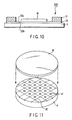
- a chuck table 8 shown in FIGS. 11 and 12 can be used.
- the chuck table 8 has suction holes 81 formed in positions corresponding to a plurality of integrated circuit elements.
- the chuck table 8 can also have trenches 82 formed in portions corresponding to scribe lines between the integrated circuit elements. It is possible to place the wafer W on the chuck table 8, fix the wafer W by suction, and cut the wafer W along the scribe lines (i.e., along the trenches 82) by the blade 51, thereby dicing the wafer W. In this dicing, the blade 51 can cut into the trenches 82.
- reference numeral 83 denotes a suction path; and 84, a suction pump.
- the chuck table 8 on which the wafer W is diced and a plurality of chips are separated from each other is moved to a testing area. In this testing area, a tester checks the electrical characteristics of the chips via the probe needles 61.
- a semiconductor substrate is cut as it is adhered to a jig. Therefore, the relative positions of integrated circuit chips do not shift from each other during cutting. After that, the electrical characteristics of these integrated circuit chips can be tested in a testing apparatus while the chips are kept placed on the jig. This increases the testing efficiency. Since the substrate holding apparatus for holding the diced substrate to be loaded into the testing apparatus has a small, low-profile structure, a conventional testing apparatus for testing a substrate before dicing can be used by making few alterations to it.
- the adhesive film wherein the adhesion of each surface is reduced when applied with energy can be used in various applications in which it is effective to selectively use an adhesive state and non-adhesive state, as the adhesive film improves the operations of dicing and testing when used in the embodiments.
Landscapes
- Engineering & Computer Science (AREA)
- Mechanical Engineering (AREA)
- Testing Or Measuring Of Semiconductors Or The Like (AREA)
- Dicing (AREA)
- Container, Conveyance, Adherence, Positioning, Of Wafer (AREA)
Abstract
Description
the first adhesive film is stretched inside a ring-like frame having a size larger than the semiconductor substrate.
applying second energy to the first surface of the adhesive film, and peeling the integrated circuit elements from the adhesive film.
separating the plurality of integrated circuit elements into individual integrated circuit elements by cutting the semiconductor substrate by cutting means, the plurality of separated integrated circuit elements being fixed to the chuck table by suction;
aligning the semiconductor substrate fixed to the chuck table by suction with a probe positioned in a space above the chuck table; and
testing the electrical characteristics of the integrated circuit elements while the probe is in contact with electrode pads of the integrated circuit elements.
Claims (17)
- A dicing method of a semiconductor substrate on which a plurality of integrated circuit elements are arranged in a matrix, the method comprises:adhering at least an entire region on the rear surface of the semiconductor substrate, which opposes a surface on which the integrated circuit elements are arranged, to a plate-like jig via at least one adhesive layer having adhesion properties, adhesion of the adhesive layer being reduced when energy is applied to the adhesive layer; andseparating the integrated circuit elements by cutting the semiconductor substrate by cutting means.
- A dicing method according to claim 1, wherein the at least one adhesive layer is an adhesive film having two adhesive surfaces.
- A dicing method according to claim 2, wherein the two surfaces of the adhesive film are first and second surfaces, and energies to be applied to reduce adhesion of the first and second surfaces are different in one of type and magnitude.
- A dicing method according to claim 3, wherein the second surface of the adhesive film is on a jig side, the first surface of the adhesive film is on a semiconductor substrate side, and the energy to be applied to the second surface to reduce the adhesion thereof is smaller than the energy to be applied to the first surface to reduce the adhesion thereof.
- A dicing method according to claim 1, wherein
the adhesive layer has a laminated structure of first and second adhesive films, the first adhesive film being adhered to the semiconductor substrate, the adhesion at a surface of the first adhesive film, which contacts the semiconductor substrate, being, reduced by application of a predetermined energy, the second adhesive film being adhered to the jig, and adhesion of two surfaces of the second adhesive film being reduced by application of energy different from the predetermined energy, and
the first adhesive film is stretched inside a ring-like frame having a size larger than the semiconductor substrate. - A testing method of a plurality of integrated circuit chips formed on a semiconductor substrate, wherein the testing method comprises:adhering a rear surface of the semiconductor substrate, which opposes a surface on which the plurality of integrated circuit chips are formed, to a plate-like jig by at least one adhesive layer formed over at least an entire region in which integrated circuit elements are arranged;cutting the semiconductor substrate by cutting means to separate the plurality of integrated circuit elements into individual integrated circuit elements, the cut semiconductor substrate being adhered on the jig by the adhesive layer;aligning the semiconductor substrate adhered on the jig with a probe positioned in a space above the jig; andtesting electrical characteristics of the integrated circuit elements while the probe is in contact with electrode pads of the integrated circuit elements.
- A testing method according to claim 6, wherein the at least one adhesive layer is an adhesive film having two adhesive surfaces.
- A testing method according to claim 7, wherein the two surfaces of the adhesive film are first and second surfaces, and energies to be applied to reduce adhesion of the first and second surfaces are different in one of type and magnitude.
- A testing method according to claim 8, wherein the second surface of the adhesive film is on a jig side, the first surface of the adhesive film is on a semiconductor substrate side, and the energy to be applied to the second surface to reduce the adhesion thereof is smaller than the energy to be applied to the first surface to reduce the adhesion thereof.
- A testing method according to claim 8, further comprising:applying first energy to the second surface of the adhesive film after the electrical characteristics of the integrated circuit elements are tested, and peeling the adhesive film from the jig; andapplying second energy to the first surface of the adhesive film, and peeling the integrated circuit elements from the adhesive film.
- A testing method according to claim 10, wherein
the adhesive layer is formed by laminating a first adhesive film which is adhered to the semiconductor substrate, and wherein adhesion of a surface adhered to the semiconductor substrate is reduced by application of a predetermined energy, and a second adhesive film which is adhered to the jig, and wherein adhesion of two surfaces is reduced by application of energy different from the predetermined energy, and
the first adhesive film is stretched inside a ring-like frame having a size larger than the semiconductor substrate. - A testing method of an integrated circuit chip, wherein the testing method comprises:fixing by suction to a chuck table a rear surface of a semiconductor substrate by suction on which a plurality of integrated circuit elements are arranged, a suction surface of the chuck table including suction holes formed in positions corresponding to positions of the integrated circuit elements, and a plurality of trenches formed in positions corresponding to scribe lines for separating the plurality of integrated circuit elements arranged on the semiconductor substrate into individual integrated circuit elements;separating the plurality of integrated circuit elements into individual integrated circuit elements by cutting the semiconductor substrate by cutting means, the plurality of separated integrated circuit elements being fixed to the chuck table by suction;aligning the semiconductor substrate fixed to the chuck table by suction with a probe positioned in a space above the chuck table; andtesting electrical characteristics of the integrated circuit elements while the probe is in contact with electrode pads of the integrated circuit elements.
- A testing method according to claim 12, wherein the rear surface of the semiconductor substrate on a surface of which the plurality of integrated circuit elements are arranged is fixed via a film to the chuck table by suction.
- A substrate holding apparatus for holding a semiconductor substrate on which a plurality of integrated circuit elements are arranged, wherein the substrate holding apparatus comprises:a frame having a size larger than the semiconductor substrate;an adhesive film stretched on said frame, one surface of said adhesive film being a surface to which a rear surface of the semiconductor substrate is adhered; anda plate-like jig, the other surface of said adhesive film being adhered to said jig.
- A substrate holding apparatus according to claim 14, wherein the two surfaces of the adhesive film are first and second surfaces, adhesion of the first and second surfaces is reduced by application of energy, and energies to be applied to reduce the adhesion of the first and second surfaces are different in one of type and magnitude.
- A substrate holding apparatus according to claim 15, wherein the second surface of said adhesive film is on a jig side, the first surface of said adhesive film is on a semiconductor substrate side, and the energy to be applied to the second surface to reduce the adhesion thereof is smaller than the energy to be applied to the first surface to reduce the adhesion thereof.
- An adhesive film having two, first and second surfaces, wherein:the first and second surfaces have an adhesive layer having adhesion properties, adhesion of said adhesive layer being reduced by application of energy; andenergy to be applied to reduce adhesion of the first surface and energy to be applied to reduce adhesion of the second surface are different in one of type and magnitude.
Applications Claiming Priority (3)
| Application Number | Priority Date | Filing Date | Title |
|---|---|---|---|
| JP2002057772A JP4137471B2 (en) | 2002-03-04 | 2002-03-04 | Dicing method, integrated circuit chip inspection method, and substrate holding apparatus |
| JP2002057772 | 2002-03-04 | ||
| PCT/JP2003/002236 WO2003075331A1 (en) | 2002-03-04 | 2003-02-27 | Dicing method, method of inspecting integrated circuit element, substrate holding device, and pressure sensitive adhesive film |
Publications (2)
| Publication Number | Publication Date |
|---|---|
| EP1484791A1 true EP1484791A1 (en) | 2004-12-08 |
| EP1484791A4 EP1484791A4 (en) | 2008-03-19 |
Family
ID=27784669
Family Applications (1)
| Application Number | Title | Priority Date | Filing Date |
|---|---|---|---|
| EP03743517A Withdrawn EP1484791A4 (en) | 2002-03-04 | 2003-02-27 | DIE CUTTING METHOD, INTEGRATED CIRCUIT ELEMENT INSPECTION METHOD, SUBSTRATE SUPPORT DEVICE, AND SELF-ADHESIVE FILM |
Country Status (7)
| Country | Link |
|---|---|
| US (1) | US8101436B2 (en) |
| EP (1) | EP1484791A4 (en) |
| JP (1) | JP4137471B2 (en) |
| KR (1) | KR100691034B1 (en) |
| CN (1) | CN1327491C (en) |
| TW (1) | TW200403736A (en) |
| WO (1) | WO2003075331A1 (en) |
Cited By (3)
| Publication number | Priority date | Publication date | Assignee | Title |
|---|---|---|---|---|
| DE102005024431A1 (en) * | 2005-05-24 | 2006-11-30 | Infineon Technologies Ag | Adhesive sheet support plate and method for producing semiconductor devices using the adhesive sheet support plate |
| WO2008007223A3 (en) * | 2006-06-27 | 2008-05-02 | Recif Technologies | Product designed to be used with handling system |
| US8471585B2 (en) | 2009-08-27 | 2013-06-25 | Tokyo Electron Limited | Method for evaluating semiconductor device |
Families Citing this family (49)
| Publication number | Priority date | Publication date | Assignee | Title |
|---|---|---|---|---|
| US20060246279A1 (en) * | 2003-04-25 | 2006-11-02 | Masakatsu Urairi | Method of producing laser-processed product and adhesive sheet, for laser processing used therefor |
| JP4093930B2 (en) * | 2003-07-17 | 2008-06-04 | 株式会社東京精密 | Frame transport prober |
| US7586060B2 (en) * | 2003-12-25 | 2009-09-08 | Nitto Denko Corporation | Protective sheet for laser processing and manufacturing method of laser processed parts |
| JP2005223244A (en) * | 2004-02-09 | 2005-08-18 | Tokyo Seimitsu Co Ltd | Tip pop-up position detection method |
| JP4381860B2 (en) * | 2004-03-24 | 2009-12-09 | 日東電工株式会社 | Method and apparatus for separating reinforcing plate fixed to reinforced semiconductor wafer |
| US7518217B2 (en) * | 2004-11-11 | 2009-04-14 | Yamaha Corporation | Semiconductor device, semiconductor wafer, chip size package, and methods of manufacturing and inspection therefor |
| CN100385691C (en) * | 2004-12-08 | 2008-04-30 | 深圳市方大国科光电技术有限公司 | Scribing method for flip-chip light-emitting diodes |
| JP4873863B2 (en) * | 2005-01-14 | 2012-02-08 | 日東電工株式会社 | Manufacturing method of laser processed product and pressure-sensitive adhesive sheet for laser processing |
| JP4854061B2 (en) * | 2005-01-14 | 2012-01-11 | 日東電工株式会社 | Manufacturing method of laser processed product and protective sheet for laser processing |
| JP2007036143A (en) * | 2005-07-29 | 2007-02-08 | Disco Abrasive Syst Ltd | Processing method of semiconductor wafer |
| JP2007088292A (en) * | 2005-09-22 | 2007-04-05 | Fujifilm Corp | Cutting method of plate member |
| JP2007095780A (en) * | 2005-09-27 | 2007-04-12 | Oki Electric Ind Co Ltd | Semiconductor device manufacturing jig and semiconductor device manufacturing method |
| KR100787721B1 (en) * | 2006-07-25 | 2007-12-24 | 제일모직주식회사 | Dicing die bond film suitable for processing thin film wafers |
| JP5196838B2 (en) * | 2007-04-17 | 2013-05-15 | リンテック株式会社 | Manufacturing method of chip with adhesive |
| JP5192790B2 (en) * | 2007-11-28 | 2013-05-08 | Towa株式会社 | Substrate cutting method and apparatus |
| JP2009272503A (en) * | 2008-05-09 | 2009-11-19 | Disco Abrasive Syst Ltd | Breaking device and breaking method for filmy adhesive |
| JP5275834B2 (en) * | 2009-02-04 | 2013-08-28 | 古河電気工業株式会社 | Wafer processing film and method for manufacturing semiconductor device using wafer processing film |
| JP5490425B2 (en) * | 2009-02-26 | 2014-05-14 | ラピスセミコンダクタ株式会社 | Method for measuring electrical characteristics of semiconductor chip |
| JP4630377B2 (en) * | 2009-03-11 | 2011-02-09 | 古河電気工業株式会社 | Manufacturing method of semiconductor device |
| DE102009013353B3 (en) * | 2009-03-16 | 2010-10-07 | Siemens Aktiengesellschaft | Method for determining armor for constant tables of placement machines |
| JP2010272639A (en) * | 2009-05-20 | 2010-12-02 | Disco Abrasive Syst Ltd | Grinding equipment |
| JP5368290B2 (en) * | 2009-12-18 | 2013-12-18 | 株式会社アドバンテスト | Carrier assembly device |
| JP5695427B2 (en) * | 2011-01-14 | 2015-04-08 | 株式会社東京精密 | Semiconductor wafer cleaving method and cleaving apparatus |
| US8409925B2 (en) * | 2011-06-09 | 2013-04-02 | Hung-Jen LEE | Chip package structure and manufacturing method thereof |
| KR20120138517A (en) | 2011-06-15 | 2012-12-26 | 삼성전자주식회사 | Apparatus for fastening chip and testing method using them |
| JP5943742B2 (en) * | 2012-07-04 | 2016-07-05 | 三菱電機株式会社 | Semiconductor test jig and semiconductor test method using the same |
| JP6043150B2 (en) * | 2012-10-29 | 2016-12-14 | 三星ダイヤモンド工業株式会社 | Breaking apparatus for laminated brittle material substrate and method for breaking laminated brittle material substrate |
| TWI549268B (en) * | 2013-02-27 | 2016-09-11 | 精材科技股份有限公司 | Wafer packaging method |
| JP6043959B2 (en) * | 2013-03-26 | 2016-12-14 | パナソニックIpマネジメント株式会社 | Semiconductor package manufacturing method, semiconductor chip support carrier, and chip mounting apparatus |
| KR101673031B1 (en) * | 2015-07-31 | 2016-11-07 | 그래핀스퀘어 주식회사 | Apparatus and method of manufacturing a graphene film |
| TW202524641A (en) * | 2016-01-15 | 2025-06-16 | 荷蘭商庫力克及索發荷蘭公司 | Placing ultra-small or ultra-thin discrete components |
| US10535572B2 (en) | 2016-04-15 | 2020-01-14 | Taiwan Semiconductor Manufacturing Company, Ltd. | Device arrangement structure assembly and test method |
| KR102523850B1 (en) * | 2016-07-11 | 2023-04-21 | 주식회사 미코세라믹스 | Chuck structure and apparatus for separating chips having the chuck structure |
| EP3533852A4 (en) * | 2016-10-27 | 2020-06-17 | Mitsui Chemicals Tohcello, Inc. | ELECTRONIC DEVICE PRODUCTION METHOD, ELECTRONIC DEVICE PRODUCTION ADHESIVE FILM, AND ELECTRONIC COMPONENT TESTING DEVICE |
| WO2018079551A1 (en) * | 2016-10-27 | 2018-05-03 | 三井化学東セロ株式会社 | Electronic device production method, adhesive film for electronic device production, and electronic component testing device |
| WO2018086698A1 (en) * | 2016-11-10 | 2018-05-17 | Applied Materials, Inc. | Holding arrangement for holding a substrate, carrier including the holding arrangement, processing system employing the carrier, and method for releasing a substrate from a holding arrangement |
| CN118471881A (en) * | 2017-08-10 | 2024-08-09 | 东京毅力科创株式会社 | Substrate processing method and substrate processing apparatus |
| JP7119310B2 (en) * | 2017-08-31 | 2022-08-17 | 富士電機株式会社 | Semiconductor test equipment |
| JP6886379B2 (en) * | 2017-09-28 | 2021-06-16 | Towa株式会社 | Holding member, manufacturing method of holding member, inspection device and cutting device |
| JP7209246B2 (en) * | 2018-09-25 | 2023-01-20 | パナソニックIpマネジメント株式会社 | Element chip manufacturing method |
| EP3924999B1 (en) | 2019-02-15 | 2026-03-25 | Kulicke & Soffa Netherlands B.V. | Dynamic release tapes for assembly of discrete components |
| CN109994416A (en) * | 2019-04-12 | 2019-07-09 | 德淮半导体有限公司 | Blue film, blue film strips and production method |
| CN110676219B (en) * | 2019-10-31 | 2021-05-25 | 合肥新汇成微电子股份有限公司 | Wafer cutting processing method for coping with vacuum abnormity |
| JP7393921B2 (en) * | 2019-11-13 | 2023-12-07 | 三井化学東セロ株式会社 | Parts manufacturing method |
| US12266558B2 (en) | 2019-12-17 | 2025-04-01 | Kulicke & Soffa Netherlands B.V. | Adhesive tapes for receiving discrete components |
| SG10201912782SA (en) * | 2019-12-20 | 2021-07-29 | Rokko Systems Pte Ltd | Post-processing system and method |
| JP7644591B2 (en) * | 2020-12-11 | 2025-03-12 | アールエム東セロ株式会社 | Manufacturing method and device for electronic components |
| KR102950734B1 (en) | 2021-05-06 | 2026-04-08 | 삼성전자주식회사 | semiconductor package for improving power integrity(PI) characteristics |
| DE102024117724A1 (en) * | 2024-06-24 | 2025-12-24 | Ams-Osram International Gmbh | DEVICE, WAFER AND METHOD FOR MANUFACTURING AN ELECTRONIC COMPONENT |
Family Cites Families (27)
| Publication number | Priority date | Publication date | Assignee | Title |
|---|---|---|---|---|
| US3399332A (en) * | 1965-12-29 | 1968-08-27 | Texas Instruments Inc | Heat-dissipating support for semiconductor device |
| US3512027A (en) * | 1967-12-12 | 1970-05-12 | Rca Corp | Encapsulated optical semiconductor device |
| US3842491A (en) * | 1972-12-08 | 1974-10-22 | Ibm | Manufacture of assorted types of lsi devices on same wafer |
| US4635092A (en) * | 1984-06-04 | 1987-01-06 | General Electric Company | Tape automated manufacture of power semiconductor devices |
| US4716124A (en) * | 1984-06-04 | 1987-12-29 | General Electric Company | Tape automated manufacture of power semiconductor devices |
| JPS62249446A (en) | 1986-04-23 | 1987-10-30 | Hitachi Ltd | Holder and usage of the same |
| JPH0831431B2 (en) * | 1987-11-11 | 1996-03-27 | 東京エレクトロン株式会社 | Inspection methods |
| CH681286A5 (en) * | 1990-04-23 | 1993-02-26 | Grapha Holding Ag | |
| US5172050A (en) * | 1991-02-15 | 1992-12-15 | Motorola, Inc. | Micromachined semiconductor probe card |
| US5487999A (en) * | 1991-06-04 | 1996-01-30 | Micron Technology, Inc. | Method for fabricating a penetration limited contact having a rough textured surface |
| US5177439A (en) * | 1991-08-30 | 1993-01-05 | U.S. Philips Corporation | Probe card for testing unencapsulated semiconductor devices |
| JPH05129431A (en) * | 1991-11-05 | 1993-05-25 | Hitachi Ltd | Adhesive tape |
| SG52223A1 (en) * | 1992-01-08 | 1998-09-28 | Murata Manufacturing Co | Component supply method |
| JP2994510B2 (en) * | 1992-02-10 | 1999-12-27 | ローム株式会社 | Semiconductor device and manufacturing method thereof |
| JPH05343517A (en) | 1992-06-10 | 1993-12-24 | Hitachi Ltd | Die sorter tape |
| US5476566A (en) * | 1992-09-02 | 1995-12-19 | Motorola, Inc. | Method for thinning a semiconductor wafer |
| JPH0974076A (en) * | 1995-09-06 | 1997-03-18 | Rohm Co Ltd | Individual separation method of light emitting semiconductor wafer |
| US6017776A (en) * | 1997-04-29 | 2000-01-25 | Micron Technology, Inc. | Method of attaching a leadframe to singulated semiconductor dice |
| US6077757A (en) * | 1997-05-15 | 2000-06-20 | Nec Corporation | Method of forming chip semiconductor devices |
| US6294439B1 (en) * | 1997-07-23 | 2001-09-25 | Kabushiki Kaisha Toshiba | Method of dividing a wafer and method of manufacturing a semiconductor device |
| US6028436A (en) * | 1997-12-02 | 2000-02-22 | Micron Technology, Inc. | Method for forming coaxial silicon interconnects |
| US6093083A (en) * | 1998-05-06 | 2000-07-25 | Advanced Imaging, Inc. | Row carrier for precision lapping of disk drive heads and for handling of heads during the slider fab operation |
| JP3341990B2 (en) | 1998-10-27 | 2002-11-05 | 株式会社東京精密 | Workpiece chuck table |
| JP2001085364A (en) * | 1999-09-14 | 2001-03-30 | Tokin Corp | Dicing method |
| JP4392732B2 (en) * | 2000-02-07 | 2010-01-06 | リンテック株式会社 | Manufacturing method of semiconductor chip |
| US6664621B2 (en) * | 2000-05-08 | 2003-12-16 | Tessera, Inc. | Semiconductor chip package with interconnect structure |
| JP2002075937A (en) * | 2000-08-30 | 2002-03-15 | Nitto Denko Corp | Semiconductor wafer processing method |
-
2002
- 2002-03-04 JP JP2002057772A patent/JP4137471B2/en not_active Expired - Fee Related
-
2003
- 2003-02-27 US US10/492,530 patent/US8101436B2/en not_active Expired - Fee Related
- 2003-02-27 EP EP03743517A patent/EP1484791A4/en not_active Withdrawn
- 2003-02-27 KR KR1020037017144A patent/KR100691034B1/en not_active Expired - Fee Related
- 2003-02-27 CN CNB038006375A patent/CN1327491C/en not_active Expired - Fee Related
- 2003-02-27 WO PCT/JP2003/002236 patent/WO2003075331A1/en not_active Ceased
- 2003-03-03 TW TW092104441A patent/TW200403736A/en not_active IP Right Cessation
Cited By (5)
| Publication number | Priority date | Publication date | Assignee | Title |
|---|---|---|---|---|
| DE102005024431A1 (en) * | 2005-05-24 | 2006-11-30 | Infineon Technologies Ag | Adhesive sheet support plate and method for producing semiconductor devices using the adhesive sheet support plate |
| DE102005024431B4 (en) * | 2005-05-24 | 2009-08-06 | Infineon Technologies Ag | Process for the production of semiconductor devices using a carrier plate with double-sided adhesive film |
| US7585701B2 (en) | 2005-05-24 | 2009-09-08 | Infineon Technologies Ag | Carrier sheet with adhesive film and method for producing semiconductor devices using the carrier sheet with adhesive film |
| WO2008007223A3 (en) * | 2006-06-27 | 2008-05-02 | Recif Technologies | Product designed to be used with handling system |
| US8471585B2 (en) | 2009-08-27 | 2013-06-25 | Tokyo Electron Limited | Method for evaluating semiconductor device |
Also Published As
| Publication number | Publication date |
|---|---|
| JP4137471B2 (en) | 2008-08-20 |
| CN1327491C (en) | 2007-07-18 |
| WO2003075331A1 (en) | 2003-09-12 |
| KR100691034B1 (en) | 2007-03-09 |
| US8101436B2 (en) | 2012-01-24 |
| CN1533594A (en) | 2004-09-29 |
| JP2003258067A (en) | 2003-09-12 |
| EP1484791A4 (en) | 2008-03-19 |
| US20050003635A1 (en) | 2005-01-06 |
| TWI309062B (en) | 2009-04-21 |
| TW200403736A (en) | 2004-03-01 |
| KR20040013001A (en) | 2004-02-11 |
Similar Documents
| Publication | Publication Date | Title |
|---|---|---|
| US8101436B2 (en) | Dicing method, method of inspecting integrated circuit element, substrate holding device, and pressure sensitive adhesive film | |
| US10889097B2 (en) | Wafer debonding system and method | |
| JP6859581B2 (en) | How to process the board | |
| US7759143B2 (en) | System and method for separating and packaging integrated circuits | |
| US7495315B2 (en) | Method and apparatus of fabricating a semiconductor device by back grinding and dicing | |
| US10269782B2 (en) | Apparatuses and methods for forming die stacks | |
| US11823965B2 (en) | Substrate processing carrier | |
| JP5515024B2 (en) | Chip laminated device inspection method, chip laminated device rearrangement unit, and chip laminated device inspection apparatus | |
| KR101113965B1 (en) | Method and apparatus for manufacturing semiconductor device, and adhesive film for it | |
| TWI899149B (en) | Method and device for the transfer of components and related light-emitting diode (led) | |
| JP4407933B2 (en) | Adhesive tape attaching method and apparatus using the same | |
| EP1209724A2 (en) | Pickup apparatus for semiconductor chips | |
| JPH11307488A (en) | Semiconductor device, manufacturing method thereof, processing guide and processing apparatus | |
| US11694937B2 (en) | Semiconductor wafer and method of probe testing | |
| TW202307947A (en) | Method of processing a substrate and system for processing a substrate | |
| US20040262722A1 (en) | Chip mounting method and mounted substrate manufacturing apparatus | |
| JPH07283295A (en) | Sheet holding jig | |
| TWI238258B (en) | Wafer testing method | |
| CN111799210A (en) | Substrate Handling Carriers | |
| JP2003086540A (en) | Semiconductor device manufacturing method and its manufacturing apparatus | |
| JPH05293795A (en) | Parts supply method | |
| JP2004281660A (en) | Semiconductor device manufacturing method and manufacturing apparatus | |
| JP2003086539A (en) | Method for manufacturing semiconductor device |
Legal Events
| Date | Code | Title | Description |
|---|---|---|---|
| PUAI | Public reference made under article 153(3) epc to a published international application that has entered the european phase |
Free format text: ORIGINAL CODE: 0009012 |
|
| 17P | Request for examination filed |
Effective date: 20041004 |
|
| AK | Designated contracting states |
Kind code of ref document: A1 Designated state(s): AT BE BG CH CY CZ DE DK EE ES FI FR GB GR HU IE IT LI LU MC NL PT SE SI SK TR |
|
| XX | Miscellaneous (additional remarks) |
Free format text: THE APPLICANT REQUESTED A CORRECTION UNDER RULE 88 EPC. |
|
| A4 | Supplementary search report drawn up and despatched |
Effective date: 20080215 |
|
| RIC1 | Information provided on ipc code assigned before grant |
Ipc: H01L 21/301 20060101AFI20030916BHEP Ipc: H01L 21/68 20060101ALI20080211BHEP Ipc: H01L 21/78 20060101ALI20080211BHEP |
|
| 17Q | First examination report despatched |
Effective date: 20090706 |
|
| STAA | Information on the status of an ep patent application or granted ep patent |
Free format text: STATUS: THE APPLICATION IS DEEMED TO BE WITHDRAWN |
|
| 18D | Application deemed to be withdrawn |
Effective date: 20091117 |