EP1482544A1 - Submount and semiconductor device - Google Patents
Submount and semiconductor device Download PDFInfo
- Publication number
- EP1482544A1 EP1482544A1 EP03743567A EP03743567A EP1482544A1 EP 1482544 A1 EP1482544 A1 EP 1482544A1 EP 03743567 A EP03743567 A EP 03743567A EP 03743567 A EP03743567 A EP 03743567A EP 1482544 A1 EP1482544 A1 EP 1482544A1
- Authority
- EP
- European Patent Office
- Prior art keywords
- layer
- solder
- submount
- substrate
- solder layer
- Prior art date
- Legal status (The legal status is an assumption and is not a legal conclusion. Google has not performed a legal analysis and makes no representation as to the accuracy of the status listed.)
- Granted
Links
Images


Classifications
-
- H—ELECTRICITY
- H01—ELECTRIC ELEMENTS
- H01S—DEVICES USING THE PROCESS OF LIGHT AMPLIFICATION BY STIMULATED EMISSION OF RADIATION [LASER] TO AMPLIFY OR GENERATE LIGHT; DEVICES USING STIMULATED EMISSION OF ELECTROMAGNETIC RADIATION IN WAVE RANGES OTHER THAN OPTICAL
- H01S5/00—Semiconductor lasers
- H01S5/02—Structural details or components not essential to laser action
- H01S5/022—Mountings; Housings
- H01S5/0235—Method for mounting laser chips
- H01S5/02355—Fixing laser chips on mounts
- H01S5/0237—Fixing laser chips on mounts by soldering
-
- H—ELECTRICITY
- H01—ELECTRIC ELEMENTS
- H01S—DEVICES USING THE PROCESS OF LIGHT AMPLIFICATION BY STIMULATED EMISSION OF RADIATION [LASER] TO AMPLIFY OR GENERATE LIGHT; DEVICES USING STIMULATED EMISSION OF ELECTROMAGNETIC RADIATION IN WAVE RANGES OTHER THAN OPTICAL
- H01S5/00—Semiconductor lasers
- H01S5/02—Structural details or components not essential to laser action
-
- H—ELECTRICITY
- H01—ELECTRIC ELEMENTS
- H01S—DEVICES USING THE PROCESS OF LIGHT AMPLIFICATION BY STIMULATED EMISSION OF RADIATION [LASER] TO AMPLIFY OR GENERATE LIGHT; DEVICES USING STIMULATED EMISSION OF ELECTROMAGNETIC RADIATION IN WAVE RANGES OTHER THAN OPTICAL
- H01S3/00—Lasers, i.e. devices using stimulated emission of electromagnetic radiation in the infrared, visible or ultraviolet wave range
- H01S3/09—Processes or apparatus for excitation, e.g. pumping
- H01S3/091—Processes or apparatus for excitation, e.g. pumping using optical pumping
- H01S3/094—Processes or apparatus for excitation, e.g. pumping using optical pumping by coherent light
- H01S3/0941—Processes or apparatus for excitation, e.g. pumping using optical pumping by coherent light of a laser diode
-
- H—ELECTRICITY
- H01—ELECTRIC ELEMENTS
- H01S—DEVICES USING THE PROCESS OF LIGHT AMPLIFICATION BY STIMULATED EMISSION OF RADIATION [LASER] TO AMPLIFY OR GENERATE LIGHT; DEVICES USING STIMULATED EMISSION OF ELECTROMAGNETIC RADIATION IN WAVE RANGES OTHER THAN OPTICAL
- H01S5/00—Semiconductor lasers
- H01S5/02—Structural details or components not essential to laser action
- H01S5/024—Arrangements for thermal management
- H01S5/02476—Heat spreaders, i.e. improving heat flow between laser chip and heat dissipating elements
-
- H—ELECTRICITY
- H10—SEMICONDUCTOR DEVICES; ELECTRIC SOLID-STATE DEVICES NOT OTHERWISE PROVIDED FOR
- H10H—INORGANIC LIGHT-EMITTING SEMICONDUCTOR DEVICES HAVING POTENTIAL BARRIERS
- H10H20/00—Individual inorganic light-emitting semiconductor devices having potential barriers, e.g. light-emitting diodes [LED]
- H10H20/80—Constructional details
- H10H20/85—Packages
- H10H20/857—Interconnections, e.g. lead-frames, bond wires or solder balls
Definitions
- the present invention relates to a submount and a semiconductor unit incorporating the submount, and more particularly to a submount for mounting a semiconductor light-emitting device on it and a semiconductor unit incorporating the submount.
- semiconductor light-emitting device is used to mean a device such as a laser diode or a light-emitting diode.
- a semiconductor unit that is provided with a semiconductor light-emitting device is commonly known. Such a semiconductor unit is produced by mounting a semiconductor light-emitting device on a submount 103 as shown in Fig. 5.
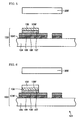
- Figures 5 and 6 are schematic cross-sectional views explaining a method of producing a conventional semiconductor unit. A method of producing a conventional semiconductor unit is explained below by referring to Fig. 5.
- a submount 103 for mounting a semiconductor light-emitting device on it is prepared.
- the submount 103 comprises:
- the Ti/Pt bi-layer 105, the Au layer 106, the solder-protecting barrier layer 107, and the solder layer 108 may be formed by using a conventional layer-forming process, such as a vapor deposition method, a sputtering method, or a plating method, or a patterning process, such as a photolithographic method or a metal mask method.
- the solder layer 108 of the submount 103 is heated and melted.
- a detector 200 detects by image processing whether or not the solder layer 108 is melted. More specifically, before the melting, the solder layer 108 reflects a large amount of light. Accordingly, the detector recognizes the color of the solder layer 108 as "white” by using the binarization in image processing. After the melting, the solder layer 108 reflects a small amount of light. Then, the detector recognizes the color of the solder layer 108 as "black.”
- a laser diode 102 as a semiconductor light-emitting device is mounted on a predetermined position on the solder layer 108 (a die-bonding step is performed). Subsequently, the solder layer 108 is cooled and solidified. This process securely bonds the laser diode 102 to the submount 103 with the solder layer 108. Then, the back side of the submount 103 is securely bonded to a heat sink (not shown in the drawing) with solder or the like to complete the production of a semiconductor unit provided with a semiconductor light-emitting device.
- the conventional semiconductor unit produced by the process shown in Figs. 5 and 6 has the following drawback.
- the detector 200 recognizes the color of the solder layer 108, if the solder layer 108 has a rough surface, the surface of the solder layer 108 reflects the light diffusely. Consequently, the detector 200 cannot obtain sufficient incident light, so that it recognizes the color of the solder layer 108 as "black.”
- the die-bonding equipment suffers an error and stops functioning or the laser diode 102 is pressed against the solder layer 108 before it is melted without successfully bonding the laser diode 102 to the submount 103.
- An object of the present invention is to offer a submount provided with a solder layer to be melted that enables the correct mounting of a semiconductor light-emitting device with high yields, and a semiconductor unit incorporating the submount.
- the present invention offers a submount comprising:
- the solder layer has a surface roughness, Ra, as small as at most 0.18 ⁇ m before it is melted, the amount of the diffuse reflection of light at the surface of the solder layer is small. Consequently, when a detector judges the color of the surface of the solder layer by image processing, it can respond with higher fidelity to the change in the state of the layer surface. As a result, the semiconductor light-emitting device can be soldered correctly with increased probability. It is more desirable that the solder layer have a surface roughness, Ra, of at most 0.15 ⁇ m before it is melted, yet more desirably at most 0.10 ⁇ m before it is melted.
- the surface roughness Ra of the solder layer is measured with a method stipulated in the Japanese Industrial Standards (JIS B 0601).
- the solder in the solder layer before it is melted have an average crystal-grain diameter of at most 3.5 ⁇ m, more desirably at most 2 ⁇ m. This reduced average crystal-grain diameter enables the further prevention of the diffuse reflection of light at the surface of the solder layer.
- the top surface of the submount substrate have a surface roughness, Ra, of at most 0.10 ⁇ m, more desirably at most 0.05 ⁇ m.
- the decrease in the surface roughness Ra of the substrate can suppress the increase in the surface roughness Ra of the solder layer resulting from the transferring of the surface unevenness of the substrate to the solder layer. As a result, the amount of the diffuse reflection of light at the surface of the solder layer can be further decreased.
- the submount may further comprise a solder-protecting barrier layer formed between the submount substrate and the solder layer.
- the submount may further comprise an electrode layer formed between the submount substrate and the solder-protecting barrier layer.
- the electrode layer can be used as an underlying layer of the solder layer.
- the submount may further comprise between the submount substrate and the solder-protecting barrier layer:
- the electrode layer is placed on the element diffusion-preventing layer.
- the submount may have a structure in which:
- the submount substrate comprise an aluminum nitride-sintered body.
- aluminum nitride has high thermal conductivity, a submount having superior heat-dissipating property can be produced.
- the present invention offers a semiconductor unit comprising:
- FIG. 1 is a schematic cross-sectional view showing an embodiment of the semiconductor unit of the present invention.
- a semiconductor unit 1 has a structure in which a laser diode 2 as a semiconductor light-emitting device is mounted on a submount 3.
- the submount 3 comprises, for example:
- the laser diode 2 is bonded to the submount 3 through the solder layer 8.
- the widths of the laser diode 2, the solder layer 8, and the solder-protecting barrier layer 7 are nearly the same.
- the solder layer 8 may have a width and a length either larger or smaller than those of the laser diode 2.
- the solder-protecting barrier layer 7 may have a width and a length either larger or smaller than those of the solder layer 8.
- the substrate 4 of the submount 3 may be made of ceramic, semiconductor, or metal.
- the types of the ceramic constituting the substrate 4 include ceramics consisting mainly of the above-described aluminum nitride (AlN), aluminum oxide (Al 2 O 3 ), silicon carbide (SiC), or silicon nitride (Si 3 N 4 ).
- the types of the semiconductor constituting the substrate 4 include silicon (Si).
- the types of the metal constituting the substrate 4 include copper (Cu), tungsten (W), molybdenum (Mo), iron (Fe), alloys comprising these, and composite materials composed of these materials.
- the substrate 4 be made of a material having high thermal conductivity. It is desirable that the substrate 4 have a thermal conductivity of at least 100 W/mK, more desirably at least 170 W/mK. In addition, it is desirable that the substrate 4 have a coefficient of thermal expansion comparable to that of the material constituting the laser diode 2. For example, when the laser diode 2 is made of a material such as gallium arsenide (GaAs) or indium phosphide (InP), it is desirable that the substrate 4 have a coefficient of thermal expansion of at most 10 ⁇ 10 -6 /K, more desirably at most 5 ⁇ 10 -6 /K.
- GaAs gallium arsenide
- InP indium phosphide
- the substrate When the substrate 4 is made of ceramic, the substrate may be provided with either a through hole that electrically connects a part of the top surface of the substrate 4 to the opposite portion in the back face or a via hole in which a conducting material (via fill) is filled.
- the conducting material (via fill) for filling the via hole consist mainly of a metal having a high melting point, particularly tungsten (W) or molybdenum (Mo).
- the above-described conducting material may also comprise, in addition to the metallic material such as tungsten or molybdenum, a transition metal such as titanium (Ti), a constituent material of glass, or a base material for forming the substrate 4 such as aluminum nitride (AlN).
- the substrate 4 have a "flatness" of at most 5 ⁇ m, more desirably at most 1 ⁇ m. If the flatness is more than 5 ⁇ m, when the laser diode 2 is bonded, gaps may be developed between the submount 3 and the laser diode 2. The gaps reduce the effect of cooling the laser diode 2.
- flatness is defined as the magnitude of the deviation from the geometrically precise plane of a plane form and is stipulated in JIS B 0621.
- the Ti layer a layer comprising titanium (Ti), constituting a part of the Ti/Pt bi-layer 5 is formed to make contact with the top surface of the substrate 4. Consequently, the Ti layer is made of a material capable of making intimate contact with the substrate 4, so that it is called an intimate-contact layer.
- the intimate-contact layer may be made of a material such as the above-described titanium (Ti), chromium (Cr), nickel-chromium (NiCr) alloy, tantalum (Ta), or a compound of these.
- the platinum (Pt) layer constituting the remaining part of the Ti/Pt bi-layer 5 is formed on the top surface of the Ti layer and is called an element diffusion-preventing layer.
- the element diffusion-preventing layer may be made of a material such as the above-described platinum (Pt), palladium (Pd), nickel-chromium (NiCr) alloy, a tungsten-titanium (TiW) compound, nickel (Ni), or molybdenum (Mo).
- the Au layer 6 is a so-called electrode layer and usually consists mainly of Au.
- the solder-protecting barrier layer 7 may be made of a material such as platinum (Pt), nickel-chromium (NiCr) alloy, or nickel (Ni).
- the solder layer 8 may be made of a material such as gold-tin (AuSn)-based solder, gold-germanium (AuGe)-based solder, lead-tin (PbSn)-based solder, indium-tin (InSn)-based solder, silver-tin (AgSn)-based solder, other alloy solder, solder produced by alloying these materials, or a laminated body composed of metals used in these alloy solders.
- solder layer 8 is made of gold-tin (AuSn)-based solder
- AuSn gold-tin
- the above-described Ti/Pt bi-layer 5, Au layer 6, solder-protecting barrier layer 7, and solder layer 8 are referred to as a metallized layer.
- These metallized layers may be formed by using conventional layer-forming methods as required. More specifically, the types of the metallized layer-forming methods include a layer-forming process, such as an vapor deposition method and a sputtering method, and a plating process.
- the above-described Ti/Pt bi-layer 5, Au layer 6, solder-protecting barrier layer 7, and solder layer 8 can be formed so as to have a specified pattern by using a patterning process.
- the types of the patterning process include a lift-off method incorporating photolithography, a chemical etching method, a dry etching method, and a metal mask method.
- the titanium (Ti) layer 5b constituting the intimate-contact layer of the Ti/Pt bi-layer 5 have a thickness of at least 0.01 ⁇ m and at most 1.0 ⁇ m. It is desirable that the platinum (Pt) layer 5a constituting the element diffusion-preventing layer of the Ti/Pt bi-layer 5 have a thickness of at least 0.01 ⁇ m and at most 1.5 ⁇ m. It is desirable that the Au layer 6 as the electrode layer have a thickness of at least 0.1 ⁇ m and at most 10 ⁇ m. It is desirable that solder-protecting barrier layer 7 have a thickness of at least 0.01 ⁇ m and at most 1.5 ⁇ m. It is desirable that the solder layer 8 have a thickness of at least 0.1 ⁇ m and at most 10 ⁇ m.
- the term "semiconductor light-emitting device” is used to mean a device such as a laser diode or a light-emitting diode.
- the semiconductor material constituting the device may be a material such as a GaAs semiconductor, an InP semiconductor, or another III-V group compound semiconductor.
- the device may be either a face-up type or a face-down type.
- the face-up-type device has a structure in which the light-emitting portion is formed at a place closer to the top surface and the light emerges either from the top surface or from a side face.
- the face-down-type device has a structure in which the light-emitting portion is formed at a place closer to the back face, which makes contact with the solder layer 8, and the light emerges from a side face.
- the face-down-type device is used as the laser diode 2 shown in Fig. 1, the light-emitting portion, which generates heat, is positioned at a place closer to the substrate 4 in comparison with the face-up-type device. Therefore, this arrangement can further improve the heat-dissipating property of the semiconductor unit 1.
- the laser diode 2 is provided on its surface with an insulating layer, such as a silicon oxide (SiO 2 ) layer, and a metallized layer as an electrode layer, such as a gold (Au) layer. It is desirable that the gold (Au) layer as the electrode layer have a thickness of at least 0.1 ⁇ m and at most 10 ⁇ m in order to secure a good wettability with the solder layer 8.
- the semiconductor unit 1 shown in Fig. 1 may be bonded to a heat sink by using solder or the like. More specifically, first, layers such as an intimate-contact layer and an element diffusion-preventing layer are formed on the back face of the substrate 4 and at the place opposite to the place where the Ti/Pt bi-layer 5 is formed on the top surface. Then, a heat sink is placed at the back-face side of the substrate 4 through sheet-shaped solder. The substrate 4 is securely bonded to the heat sink through the solder placed at the back-face side of the substrate 4.
- the solder for bonding the substrate 4 to the heat sink may be the above-described sheet-shaped solder (solder foil). Alternatively, a layer of solder may be placed on the top surface of the heat sink in advance. Yet alternatively, a solder layer may be formed on the metallized layer on the back face of the substrate 4. In this case, it is desirable that the laser diode 2 and the heat sink be bonded concurrently to the substrate 4.
- the heat sink may be made of a material such as metal or ceramic.
- the types of the metal constituting the heat sink include copper (Cu), tungsten (W), molybdenum (Mo), iron (Fe), alloys comprising these metals, and composite materials composed of these materials. It is desirable to form on the surface of the heat sink a nickel (Ni) layer, a gold (Au) layer, or a layer comprising the foregoing metal. These layers can be formed by the vapor deposition method and the plating method. It is desirable that the heat sink have a thermal conductivity as high as at least 100 W/mK.
- Figure 2 is a schematic cross-sectional view explaining the method of producing the semiconductor unit shown in Fig. 1.
- the first step is the production of the substrate.
- the substrate may have a width of 50 mm, a length of 50 mm, and a thickness of 0.4 mm, for example.
- the substrate has a size larger than that of the substrate 4 of the submount 3.
- a required structure is formed on the surface of the substrate.
- the substrate is cut and separated in the below-mentioned cutting step to obtain the submount 3.
- the substrate to be used as the substrate 4 of the submount 3 is produced according to an ordinary substrate production method.
- the substrate 4 is made of an aluminum nitride (AlN)-sintered body.
- the substrate 4 made of ceramic, such as an aluminum nitride-sintered body, may be produced by applying a method for producing an ordinary ceramic structure.
- the second step is the lapping or polishing of the surface of the substrate made of an aluminum nitride-sintered body and produced in the first step, the substrate production step. It is desirable that the aluminum nitride substrate to be used as the substrate 4 be lapped or polished so as to attain a surface roughness, Ra, of at most 0.10 ⁇ m, more desirably at most 0.05 ⁇ m.
- the lapping or polishing operation may be performed by applying an ordinary method, such as the lapping with sandpaper or the polishing with abrasives. Alternatively, a grinding machine or the sandblasting may be employed.
- the third step is to provide a pattern for forming with a specified pattern the Ti layer 5b as an intimate-contact layer, the Pt layer 5a as an element diffusion-preventing layer, and the Au layer 6 as an electrode layer all as shown in Fig. 2.
- the other region than the region for forming the Ti layer 5b, the Pt layer 5a, and the Au layer 6 on the surface of the substrate is provided with a resist layer by using the photolithographic method.
- the fourth step is to vapor-deposit an intimate-contact layer. More specifically, a Ti layer to be used as the Ti layer 5b as an intimate-contact layer is vapor-deposited on the surface of the substrate.
- the formed Ti layer may have a thickness of 0.1 ⁇ m, for example.
- the fifth step is to form a Pt layer to be used as the Pt layer 5a as an element diffusion-preventing layer on the Ti layer to be used as the Ti layer 5b as an intimate-contact layer.
- the Pt layer may have a thickness of 0.2 ⁇ m, for example.
- the sixth step is to form the Au layer 6 as an electrode layer by the vapor deposition method.
- the Au layer may have a thickness of 0.6 ⁇ m, for example.
- the seventh step is a lift-off step.
- the resist layer formed in the third step a patterning step, is removed with a resist-removing liquid together with the part of the Ti layer, the Pt layer, and the Au layer positioned on the resist layer.
- the removal can form the Ti layer 5b, the Pt layer 5a, and the Au layer 6 all having the specified pattern on the surface of the substrate.
- the eighth step is to form the solder-protecting barrier layer 7.
- the solder-protecting barrier layer 7 made of platinum (Pt) is formed on the Au layer 6 by using the metal mask method.
- the solder-protecting barrier layer 7 has a thickness of 0.2 ⁇ m.
- the ninth step is to form the solder layer 8 on the solder-protecting barrier layer 7 by the vapor deposition method.
- the decrease in the pressure (ultimate vacuum degree) of the atmosphere in the chamber before the layer formation decreases the crystal-grain diameter of the solder. It is desirable that the ultimate vacuum degree be at most 5.0 ⁇ 10 -4 Pa. If it exceeds 5.0 ⁇ 10 -4 Pa, impurity gases such as water vapor and oxygen tend to remain in the solder layer. As a result, foreign matters having a large particle diameter may be included in the solder layer 8. It is more desirable that the ultimate vacuum degree be at most 1.0 ⁇ 10 -4 Pa.
- the crystal-grain diameter and the surface roughness Ra can be varied. It is desirable that the layer-forming rate be at least 0.1 nm/s and at most 1.0 nm/s, more desirably at least 0.3 nm/s and at most 0.7 nm/s. If it is less than 0.1 nm/s, the growth of the nucleus is promoted, increasing the crystal-grain diameter. Consequently, the surface roughness Ra is also increased. If it is more than 1.0 nm/s, the temperature of the substrate rises, causing the crystal-grain diameter to tend to increase due to the below-described reason. As a result, the surface roughness Ra tends to increase.
- the crystal-grain diameter and the surface roughness Ra can be varied. It is desirable that the temperature be at least 20 °C and at most 150 °C, more desirably at least 20 °C and at most 120 °C. If it is more than 150 °C, the temperature of the substrate rises, promoting the growth of the nucleus. As a result, the crystal-grain diameter increases, increasing the surface roughness Ra.
- the solder layer 8 having a specified pattern may be formed by the metal mask method. Alternatively, it may be formed by the photolithographic method as shown in the third to seventh steps of the method of producing the semiconductor unit of the present invention.
- the tenth step is to cut the substrate prepared in the first step on the surface of which the specified structure is formed as described above. After the cutting, the submount 3 shown in Fig. 1 is obtained.
- the eleventh step is to bond the laser diode 2 as a semiconductor light-emitting device to the submount 3.
- the solder layer 8 is melted by heating.
- a detector 200 detects by image processing whether or not the solder layer 8 is melted. More specifically, the illumination intensity of the light incident upon the detector is divided into 256 levels of gray, for example. The level of the darkest portion in the substrate 4 is defined as "0,” and the brightest portion in the Au layer 6 as "255.” When the level of gray of the light incident from the solder layer 8 exceeds "50,” its color is recognized as "white” and the solder layer 8 is judged to be unmolten.
- the binarization in image processing judges whether or not the solder layer 8 is molten.
- the laser diode 2 is placed on the solder layer 8 judged to be molten.
- the laser diode 2 a chip made of GaAs, is bonded to the submount 3 through the solder layer 8. This completes the production of the semiconductor unit 1 shown in Fig. 1.
- the surface 8f of the solder layer 8 has a surface roughness, Ra, as small as 0.18 ⁇ m before it is melted as described below. Consequently, the diffuse reflection of light at the surface of the solder layer 8 can be suppressed, so that a sufficient amount of the reflected light can enter the detector 200. In the die-bonding step, this sufficient amount of light can significantly reduce the probability that the detector 200 would misjudge the solder layer 8 before melting to be "black,” i.e., "molten.” In other words, whether or not the solder layer 8 is molten can be judged correctly with higher probability. As a result, the laser diode 2 can be soldered to the submount 3 in good timing while the solder layer is molten.
- Samples 1 to 30 were produced by the below-described procedure. Samples 1 to 20 were produced as Examples, and Samples 21 to 30 were produced as Comparative examples. Sample No. Category of Sample Composition of solder Ultimate vacuum degree ( ⁇ 10 -4 Pa) Layer-forming rate (nm/s) Temperature of substrate 4 (°C) 1
- aluminum nitride-sintered bodies having a width of 50 mm, a length of 50 mm, and a thickness of 0.4 mm were prepared as a substrate.
- the surface of individual sintered bodies was polished to cause the top surface 4f to have the surface roughness Ra as shown in Table II.
- Operations using the lift-off method incorporating photolithography and the vapor deposition method formed a metallized layer comprising the Ti layer 5b having a thickness of 0.1 ⁇ m, the Pt layer 5a of 0.2 ⁇ m, and the Au layer 6 of 0.6 ⁇ m.
- Samples other than Samples 10, 11, 12, and 27 were provided with a solder-protecting barrier layer 7, made of platinum, having a thickness of 0.2 ⁇ m on the metallized layer by using the metal mask and vapor deposition methods.
- composition of solder shows the weight ratio of the elements constituting the solder layer 8. Twenty submounts having a width of 1.2 mm, a length of 1.5 mm, and a thickness of 0.3 mm were obtained from each of Samples 1 to 30 by cutting the substrate 4. The proportion of the successful image processing by the detector 200 at the time of the soldering of the laser diode 2 was examined for each Sample. The results are also shown in Table II.
- solder constituting the solder layer 8 have an average crystal-grain diameter of at most 3.5 ⁇ m, more desirably at most 2.0 ⁇ m. It is desirable that the top surface 4f of the substrate 4 have a surface roughness, Ra, of at most 0.10 ⁇ m, more desirably at most 0.05 ⁇ m.
- Sample 1 one of Examples of the present invention, was subjected to the following test.
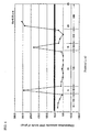
- the detector 200 measured the intensity (illumination intensity) of light reflected from the substrate 4 as the submount substrate, from the solder layer 8 before it is melted, and from the Au layer 6. A part of the result is shown in Fig. 3.
- the axis of ordinates shows the illumination intensity of the reflected light in 256 levels of gray
- the axis of abscissas shows the position of the submount.
- the numerals "4,” “8,” and “6” respectively show the substrate 4, the solder layer 8, and the Au layer 6 illustrated in Figs. 1 and 2, and the axis of ordinates shows the intensity of light reflected from individual positions.
- the detector 200 can easily recognize the state of solder layer 8 as being unmolten.
- Sample 21 one of Comparative examples, was also subjected to the foregoing test.
- the detector 200 measured the intensity (illumination intensity) of light reflected from the substrate 104, from the solder layer 108 before it is melted, and from the Au layer 106. A part of the result is shown in Fig. 4.
- the axis of ordinates shows the illumination intensity of the reflected light in 256 levels of gray
- the axis of abscissas shows the position of the submount.
- the numerals "104,” “108,” and “106” respectively show the substrate 104, the solder layer 108, and the Au layer 106 illustrated in Figs. 5 and 6, and the axis of ordinates shows the intensity of light reflected from individual positions.
- the present invention can offer a submount that can reliably mount a semiconductor light-emitting device on it by recognizing the melting of the solder layer with a detector, and a semiconductor unit incorporating the submount.
Landscapes
- Physics & Mathematics (AREA)
- Electromagnetism (AREA)
- Optics & Photonics (AREA)
- Condensed Matter Physics & Semiconductors (AREA)
- General Physics & Mathematics (AREA)
- Engineering & Computer Science (AREA)
- Plasma & Fusion (AREA)
- Semiconductor Lasers (AREA)
- Led Device Packages (AREA)
- Die Bonding (AREA)
Abstract
Description
| Sample No. | Category of Sample | Composition of solder | Ultimate vacuum degree ( × 10-4 Pa) | Layer-forming rate (nm/s) | Temperature of substrate 4 (°C) |
| 1 | Example | Au:Sn = 80:20 | 0.8 | 0.5 | 80 |
| 2 | Au:Sn = 80:20 | 1.5 | 0.5 | 80 | |
| 3 | Au:Sn = 80:20 | 4.0 | 0.5 | 80 | |
| 4 | Au:Sn = 80:20 | 0.8 | 0.2 | 80 | |
| 5 | Au:Sn = 80:20 | 0.8 | 0.8 | 80 | |
| 6 | Au:Sn = 80:20 | 0.8 | 0.5 | 50 | |
| 7 | Au:Sn = 80:20 | 0.8 | 0.5 | 130 | |
| 8 | Au:Sn = 80:20 | 0.8 | 0.5 | 80 | |
| 9 | Au:Sn = 80:20 | 0.8 | 0.5 | 80 | |
| 10 | Au:Sn = 80:20 | 0.8 | 0.5 | 80 | |
| 11 | Au:Sn = 80:20 | 1.1 | 0.6 | 100 | |
| 12 | Au:Sn = 80:20 | 3.0 | 0.8 | 130 | |
| 13 | Au:Sn = 80:20 | 3.0 | 0.8 | 80 | |
| 14 | Au:Sn = 80:20 | 3.0 | 0.5 | 130 | |
| 15 | Au:Sn = 80:20 | 0.8 | 0.8 | 130 | |
| 16 | Au:Sn = 10:90 | 0.8 | 0.5 | 80 | |
| 17 | Au:Sn = 10:90 | 3.0 | 0.8 | 130 | |
| 18 | Au:Sn = 10:90 | 3.0 | 0.5 | 80 | |
| 19 | Au:Sn = 10:90 | 0.8 | 0.2 | 80 | |
| 20 | Au:Sn = 10:90 | 0.8 | 0.5 | 130 | |
| 21 | Comparative example | Au:Sn = 80:20 | 8.0 | 0.05 | 170 |
| 22 | Au:Sn = 80:20 | 6.0 | 0.5 | 80 | |
| 23 | Au:Sn = 80:20 | 0.8 | 0.05 | 80 | |
| 24 | Au:Sn = 80:20 | 0.8 | 1.2 | 80 | |
| 25 | Au:Sn = 80:20 | 0.8 | 0.5 | 170 | |
| 26 | Au:Sn = 80:20 | 0.8 | 0.5 | 80 | |
| 27 | Au:Sn = 80:20 | 6.0 | 0.5 | 80 | |
| 28 | Au:Sn = 10:90 | 6.0 | 0.5 | 80 | |
| 29 | Au:Sn = 10:90 | 0.8 | 1.2 | 80 | |
| 30 | Au:Sn = 10:90 | 0.8 | 0.5 | 170 |
| Sample No. | Category of Sample | Presence or absence of solder-protecting | Surface roughness Ra of (µm) | Surface roughness Ra of (µm) | Average crystal-grain diameter of (µm) | Successful image processing |
| 1 | Example | ○ | 0.04 | 0.08 | 1.3 | 20/20 |
| 2 | ○ | 0.04 | 0.12 | 2.3 | 19/20 | |
| 3 | ○ | 0.04 | 0.15 | 3.0 | 18/20 | |
| 4 | ○ | 0.04 | 0.14 | 2.8 | 18/20 | |
| 5 | ○ | 0.04 | 0.13 | 2.7 | 19/20 | |
| 6 | ○ | 0.04 | 0.08 | 1.2 | 20/20 | |
| 7 | ○ | 0.04 | 0.15 | 3.0 | 17/20 | |
| 8 | ○ | 0.06 | 0.11 | 1.4 | 19/20 | |
| 9 | ○ | 0.08 | 0.12 | 1.3 | 19/20 | |
| 10 | × | 0.04 | 0.08 | 1.3 | 20/20 | |
| 11 | × | 0.04 | 0.13 | 2.6 | 18/20 | |
| 12 | × | 0.08 | 0.18 | 3.4 | 16/20 | |
| 13 | ○ | 0.04 | 0.16 | 3.2 | 17/20 | |
| 14 | ○ | 0.04 | 0.17 | 3.3 | 16/20 | |
| 15 | ○ | 0.04 | 0.16 | 3.2 | 16/20 | |
| 16 | ○ | 0.04 | 0.09 | 1.4 | 20/20 | |
| 17 | ○ | 0.08 | 0.17 | 3.3 | 17/20 | |
| 18 | ○ | 0.04 | 0.14 | 2.7 | 19/20 | |
| 19 | ○ | 0.04 | 0.14 | 2.8 | 19/20 | |
| 20 | ○ | 0.04 | 0.15 | 3.1 | 18/20 | |
| 21 | Comparative example | ○ | 0.12 | 0.32 | 6.2 | 0/20 |
| 22 | ○ | 0.04 | 0.20 | 3.8 | 10/20 | |
| 23 | ○ | 0.04 | 0.25 | 4.9 | 4/20 | |
| 24 | ○ | 0.04 | 0.22 | 4.2 | 7/20 | |
| 25 | ○ | 0.04 | 0.23 | 4.5 | 5/20 | |
| 26 | ○ | 0.12 | 0.20 | 1.4 | 11/20 | |
| 27 | × | 0.04 | 0.21 | 4.2 | 8/20 | |
| 28 | ○ | 0.04 | 0.21 | 4.1 | 8/20 | |
| 29 | ○ | 0.04 | 0.23 | 4.4 | 6/20 | |
| 30 | ○ | 0.04 | 0.23 | 4.5 | 5/20 | |
| Note: In the "Presence or absence of solder-protecting barrier layer 7," the sign "○" shows the presence of the solder-protecting barrier layer 7, and the sign "×" shows the absence of the solder-protecting barrier layer 7. |
Claims (11)
- A submount, comprising:(a) a submount substrate; and(b) a solder layer that:(b1) is formed on the top surface of the submount substrate; and(b2) has a surface roughness, Ra, of at most 0.18 µm before the solder layer is melted.
- A submount as defined by claim 1, wherein the solder layer has a surface roughness, Ra, of at most 0.15 µm before it is melted.
- A submount as defined by claim 1, wherein the solder layer has a surface roughness, Ra, of at most 0.10 µm before it is melted.
- A submount as defined by any one of claims 1 to 3, wherein the solder in the solder layer has an average crystal-grain diameter of at most 3.5 µm before it is melted.
- A submount as defined by any one of claims 1 to 4, wherein the top surface of the submount substrate has a surface roughness, Ra, of at most 0.10 µm.
- A submount as defined by any one of claims 1 to 5, the submount further comprising a solder-protecting barrier layer formed between the submount substrate and the solder layer.
- A submount as defined by claim 6, the submount further comprising an electrode layer formed between the submount substrate and the solder-protecting barrier layer.
- A submount as defined by claim 7, the submount further comprising between the submount substrate and the solder-protecting barrier layer:the electrode layer being placed on the element diffusion-preventing layer.(a) an intimate-contact layer formed such that it makes contact with the top surface of the submount substrate; and(b) an element diffusion-preventing layer formed on the intimate-contact layer;
- A submount as defined by claim 8, wherein:(a) the intimate-contact layer comprises titanium;(b) the element diffusion-preventing layer comprises platinum;(c) the electrode layer comprises gold;(d) the solder-protecting barrier layer comprises platinum; and(e) the solder layer comprises gold-tin-based solder.
- A submount as defined by any one of claims 1 to 9, wherein the submount substrate comprises an aluminum nitride-sintered body.
- A semiconductor unit incorporating a submount as defined by any one of claims 1 to 10, the semiconductor unit being provided with a semiconductor light-emitting device mounted on the solder layer.
Applications Claiming Priority (3)
| Application Number | Priority Date | Filing Date | Title |
|---|---|---|---|
| JP2002060764A JP3982284B2 (en) | 2002-03-06 | 2002-03-06 | Submount and semiconductor device |
| JP2002060764 | 2002-03-06 | ||
| PCT/JP2003/002451 WO2003075341A1 (en) | 2002-03-06 | 2003-03-03 | Submount and semiconductor device |
Publications (3)
| Publication Number | Publication Date |
|---|---|
| EP1482544A1 true EP1482544A1 (en) | 2004-12-01 |
| EP1482544A4 EP1482544A4 (en) | 2006-09-27 |
| EP1482544B1 EP1482544B1 (en) | 2016-11-30 |
Family
ID=27784815
Family Applications (1)
| Application Number | Title | Priority Date | Filing Date |
|---|---|---|---|
| EP03743567.4A Expired - Lifetime EP1482544B1 (en) | 2002-03-06 | 2003-03-03 | Submount and semiconductor device |
Country Status (7)
| Country | Link |
|---|---|
| US (1) | US7298049B2 (en) |
| EP (1) | EP1482544B1 (en) |
| JP (1) | JP3982284B2 (en) |
| KR (1) | KR100957669B1 (en) |
| CN (1) | CN1298032C (en) |
| AU (1) | AU2003211502A1 (en) |
| WO (1) | WO2003075341A1 (en) |
Cited By (2)
| Publication number | Priority date | Publication date | Assignee | Title |
|---|---|---|---|---|
| EP1868241A4 (en) * | 2005-03-18 | 2012-02-15 | Dowa Electronics Materials Co Ltd | AUXILIARY MOUNTING AND METHOD OF MANUFACTURING THE SAME |
| WO2018158341A1 (en) * | 2017-03-01 | 2018-09-07 | Osram Opto Semiconductors Gmbh | Method for fastening a semiconductor chip on a lead frame, and electronic component |
Families Citing this family (42)
| Publication number | Priority date | Publication date | Assignee | Title |
|---|---|---|---|---|
| JP3509809B2 (en) * | 2002-04-30 | 2004-03-22 | 住友電気工業株式会社 | Submount and semiconductor device |
| JP3882712B2 (en) | 2002-08-09 | 2007-02-21 | 住友電気工業株式会社 | Submount and semiconductor device |
| JP3803339B2 (en) * | 2003-01-10 | 2006-08-02 | 松下電器産業株式会社 | Semiconductor laser device |
| KR100593536B1 (en) | 2004-03-08 | 2006-06-28 | 엘지전자 주식회사 | Manufacturing method of light emitting diode |
| JP4228303B2 (en) * | 2004-04-12 | 2009-02-25 | 住友電気工業株式会社 | Semiconductor light emitting element mounting member and semiconductor light emitting device using the same |
| JP2006093486A (en) * | 2004-09-27 | 2006-04-06 | Kyocera Corp | Light emitting element mounting substrate and light emitting device |
| KR100862457B1 (en) * | 2004-12-29 | 2008-10-08 | 삼성전기주식회사 | Flip chip bonding structure of light emitting device using metal column |
| JP5166017B2 (en) * | 2005-02-07 | 2013-03-21 | 株式会社東芝 | Manufacturing method of ceramic wiring board and manufacturing method of semiconductor device using the same |
| JP5062545B2 (en) * | 2005-03-31 | 2012-10-31 | Dowaエレクトロニクス株式会社 | Submount and manufacturing method thereof |
| JP2006286943A (en) * | 2005-03-31 | 2006-10-19 | Dowa Mining Co Ltd | Submount substrate and manufacturing method thereof |
| JP2006286944A (en) * | 2005-03-31 | 2006-10-19 | Dowa Mining Co Ltd | Submount and manufacturing method thereof |
| JP2006261569A (en) * | 2005-03-18 | 2006-09-28 | Dowa Mining Co Ltd | Submount and manufacturing method thereof |
| JP4618790B2 (en) * | 2005-04-07 | 2011-01-26 | 田中貴金属工業株式会社 | Hermetic seal cover and method for manufacturing the same |
| KR101065076B1 (en) * | 2005-05-07 | 2011-09-15 | 삼성전자주식회사 | Submount for Light-Emitting Device Package |
| KR100598357B1 (en) | 2005-05-24 | 2006-07-06 | 엘지전자 주식회사 | Submount Substrate for Light-Emitting Element |
| JP2006332435A (en) * | 2005-05-27 | 2006-12-07 | Sharp Corp | Submount, semiconductor laser device and manufacturing method thereof, hologram laser device, and optical pickup device |
| KR20060131327A (en) * | 2005-06-16 | 2006-12-20 | 엘지전자 주식회사 | Manufacturing method of light emitting diode |
| DE102005033469B4 (en) * | 2005-07-18 | 2019-05-09 | Infineon Technologies Ag | Method for producing a semiconductor module |
| JP4969087B2 (en) * | 2005-11-28 | 2012-07-04 | スタンレー電気株式会社 | Eutectic bonding light emitting device and manufacturing method thereof |
| JP2007201420A (en) * | 2005-12-27 | 2007-08-09 | Sharp Corp | Semiconductor light emitting device, semiconductor light emitting element, and method for manufacturing semiconductor light emitting device |
| JP2007194385A (en) * | 2006-01-19 | 2007-08-02 | Stanley Electric Co Ltd | Semiconductor light emitting device and method for manufacturing semiconductor light emitting device |
| JP2007251142A (en) * | 2006-02-14 | 2007-09-27 | Dowa Electronics Materials Co Ltd | Solder layer, electronic device bonding substrate using the same, and manufacturing method thereof |
| JP2007294899A (en) | 2006-03-31 | 2007-11-08 | Dowa Electronics Materials Co Ltd | Solder layer, electronic device bonding substrate using the same, and electronic device bonding submount |
| JP4836769B2 (en) * | 2006-12-18 | 2011-12-14 | スタンレー電気株式会社 | Semiconductor light emitting device and manufacturing method thereof |
| JP2009176805A (en) * | 2008-01-22 | 2009-08-06 | Tekcore Co Ltd | Surface roughening method for light emitting diode substrate |
| US8207547B2 (en) * | 2009-06-10 | 2012-06-26 | Brudgelux, Inc. | Thin-film LED with P and N contacts electrically isolated from the substrate |
| US9437785B2 (en) * | 2009-08-10 | 2016-09-06 | Cree, Inc. | Light emitting diodes including integrated backside reflector and die attach |
| JP5349416B2 (en) * | 2010-07-08 | 2013-11-20 | 京セラ株式会社 | Light emitting element mounting substrate and light emitting device |
| JP2010263251A (en) * | 2010-08-25 | 2010-11-18 | Sanyo Electric Co Ltd | Light-emitting device and method of manufacturing the same |
| IN2014DN06962A (en) * | 2012-02-14 | 2015-04-10 | Mitsubishi Materials Corp | |
| JP5962522B2 (en) * | 2012-03-22 | 2016-08-03 | 日亜化学工業株式会社 | Semiconductor laser device |
| US8866041B2 (en) * | 2012-04-12 | 2014-10-21 | Tdk Corporation | Apparatus and method of manufacturing laser diode unit utilizing submount bar |
| JP2013236010A (en) | 2012-05-10 | 2013-11-21 | Mitsubishi Electric Corp | Semiconductor device |
| US9070387B1 (en) | 2013-08-23 | 2015-06-30 | Western Digital Technologies, Inc. | Integrated heat-assisted magnetic recording head/laser assembly |
| US9042048B1 (en) | 2014-09-30 | 2015-05-26 | Western Digital (Fremont), Llc | Laser-ignited reactive HAMR bonding |
| JP6710083B2 (en) * | 2015-08-27 | 2020-06-17 | 西村陶業株式会社 | Heat radiating member, power semiconductor module, and LED package |
| GB201621690D0 (en) * | 2016-12-20 | 2017-02-01 | Element Six Tech Ltd | A heat sink comprising synthetic diamond material |
| JP2019145568A (en) * | 2018-02-16 | 2019-08-29 | 京セラ株式会社 | Package for light emitting element storage, light emitting device, and light emitting module |
| JP6512375B1 (en) * | 2018-04-03 | 2019-05-15 | 三菱電機株式会社 | Semiconductor device manufacturing method |
| JP7406417B2 (en) * | 2020-03-18 | 2023-12-27 | シチズンファインデバイス株式会社 | Electrode structure and bonded structure equipped with the electrode structure |
| CN114908320A (en) * | 2022-04-14 | 2022-08-16 | 广东工业大学 | An etching-free semiconductor laser heat sink structure and its preparation method and application |
| US20240304461A1 (en) * | 2023-03-07 | 2024-09-12 | Tong Hsing Electronic Industries, Ltd. | Ceramic submount for semiconductor device and method for manufacturing the same |
Family Cites Families (22)
| Publication number | Priority date | Publication date | Assignee | Title |
|---|---|---|---|---|
| JP2606716B2 (en) | 1988-01-29 | 1997-05-07 | 株式会社トーキン | Method of forming metal layer on aluminum nitride surface |
| JPH0448213A (en) * | 1990-06-15 | 1992-02-18 | Taikisha Ltd | On-floor facility body with moving body position detecting function |
| JPH0548213A (en) | 1991-08-15 | 1993-02-26 | Tanaka Kikinzoku Kogyo Kk | Sub-mount for semiconductor laser |
| JP3190718B2 (en) * | 1992-01-14 | 2001-07-23 | 株式会社東芝 | Submount for semiconductor laser |
| JPH06285622A (en) | 1993-04-02 | 1994-10-11 | Mitsubishi Materials Corp | Soldering method |
| JPH0982760A (en) * | 1995-07-07 | 1997-03-28 | Toshiba Corp | Semiconductor device, semiconductor element, and solder connection inspection method thereof |
| JP3165779B2 (en) | 1995-07-18 | 2001-05-14 | 株式会社トクヤマ | Submount |
| EP0774684A3 (en) * | 1995-11-16 | 1998-04-22 | Matsushita Electric Industrial Co., Ltd. | Optical apparatus and method for producing the same |
| JPH09316643A (en) * | 1996-02-15 | 1997-12-09 | Mitsubishi Materials Corp | Anti-deposition parts for physical vapor deposition equipment |
| JPH1065291A (en) | 1996-08-22 | 1998-03-06 | Tec Corp | Wiring board and marking method on wiring board |
| US6327289B1 (en) * | 1997-09-02 | 2001-12-04 | Matsushita Electric Industrial Co., Ltd. | Wavelength-variable semiconductor laser, optical integrated device utilizing the same, and production method thereof |
| JP3720973B2 (en) * | 1998-03-16 | 2005-11-30 | 新日本製鐵株式会社 | Diffusion bonded metal carrier and manufacturing method thereof |
| US6742701B2 (en) * | 1998-09-17 | 2004-06-01 | Kabushiki Kaisha Tamura Seisakusho | Bump forming method, presoldering treatment method, soldering method, bump forming apparatus, presoldering treatment device and soldering apparatus |
| JP2000121836A (en) * | 1998-10-09 | 2000-04-28 | Sony Corp | Light source device, illumination method and device, and optical device |
| US6903376B2 (en) * | 1999-12-22 | 2005-06-07 | Lumileds Lighting U.S., Llc | Selective placement of quantum wells in flipchip light emitting diodes for improved light extraction |
| US6853074B2 (en) * | 1999-12-27 | 2005-02-08 | Matsushita Electric Industrial Co., Ltd. | Electronic part, an electronic part mounting element and a process for manufacturing such the articles |
| JP4409041B2 (en) * | 2000-04-19 | 2010-02-03 | 株式会社東芝 | Submount material |
| DE10025032A1 (en) * | 2000-05-20 | 2001-11-29 | Dmc2 Degussa Metals Catalysts | Process for the autothermal, catalytic steam reforming of hydrocarbons |
| JP2001332651A (en) | 2000-05-24 | 2001-11-30 | Kyocera Corp | Substrate for mounting electronic components |
| US6740906B2 (en) * | 2001-07-23 | 2004-05-25 | Cree, Inc. | Light emitting diodes including modifications for submount bonding |
| JP3779218B2 (en) | 2002-02-18 | 2006-05-24 | 住友電気工業株式会社 | Submount and semiconductor device |
| US6767749B2 (en) * | 2002-04-22 | 2004-07-27 | The United States Of America As Represented By The Secretary Of The Navy | Method for making piezoelectric resonator and surface acoustic wave device using hydrogen implant layer splitting |
-
2002
- 2002-03-06 JP JP2002060764A patent/JP3982284B2/en not_active Expired - Lifetime
-
2003
- 2003-03-03 US US10/506,510 patent/US7298049B2/en not_active Expired - Lifetime
- 2003-03-03 KR KR1020047013738A patent/KR100957669B1/en not_active Expired - Fee Related
- 2003-03-03 EP EP03743567.4A patent/EP1482544B1/en not_active Expired - Lifetime
- 2003-03-03 WO PCT/JP2003/002451 patent/WO2003075341A1/en not_active Ceased
- 2003-03-03 AU AU2003211502A patent/AU2003211502A1/en not_active Abandoned
- 2003-03-03 CN CNB038039443A patent/CN1298032C/en not_active Expired - Fee Related
Cited By (5)
| Publication number | Priority date | Publication date | Assignee | Title |
|---|---|---|---|---|
| EP1868241A4 (en) * | 2005-03-18 | 2012-02-15 | Dowa Electronics Materials Co Ltd | AUXILIARY MOUNTING AND METHOD OF MANUFACTURING THE SAME |
| CN101916746B (en) * | 2005-03-18 | 2012-06-20 | 同和电子科技有限公司 | Submount and method for manufacturing same |
| WO2018158341A1 (en) * | 2017-03-01 | 2018-09-07 | Osram Opto Semiconductors Gmbh | Method for fastening a semiconductor chip on a lead frame, and electronic component |
| DE102017104276B4 (en) | 2017-03-01 | 2020-01-16 | Osram Opto Semiconductors Gmbh | Method for fastening a semiconductor chip on a lead frame and electronic component |
| US11127602B2 (en) | 2017-03-01 | 2021-09-21 | Osram Oled Gmbh | Method of fastening a semiconductor chip on a lead frame, and electronic component |
Also Published As
| Publication number | Publication date |
|---|---|
| KR20040093094A (en) | 2004-11-04 |
| WO2003075341A1 (en) | 2003-09-12 |
| JP3982284B2 (en) | 2007-09-26 |
| AU2003211502A1 (en) | 2003-09-16 |
| EP1482544B1 (en) | 2016-11-30 |
| US20050067636A1 (en) | 2005-03-31 |
| KR100957669B1 (en) | 2010-05-12 |
| US7298049B2 (en) | 2007-11-20 |
| CN1633706A (en) | 2005-06-29 |
| JP2003258360A (en) | 2003-09-12 |
| CN1298032C (en) | 2007-01-31 |
| EP1482544A4 (en) | 2006-09-27 |
Similar Documents
| Publication | Publication Date | Title |
|---|---|---|
| EP1482544B1 (en) | Submount and semiconductor device | |
| US7015583B2 (en) | Submount and semiconductor device | |
| US7518155B2 (en) | Light emitting element mounting member, and semiconductor device using the same | |
| US7196356B2 (en) | Submount and semiconductor device | |
| US6084895A (en) | Semiconductor laser apparatus | |
| CN100511735C (en) | Semiconductor device, manufacture method and electronic component unit thereof | |
| EP2521173A2 (en) | Submount and method of manufacturing the same | |
| JP2006261569A (en) | Submount and manufacturing method thereof | |
| JP3912130B2 (en) | Submount | |
| JP2007134744A (en) | Submount and semiconductor device | |
| JP3779218B2 (en) | Submount and semiconductor device | |
| JP5062545B2 (en) | Submount and manufacturing method thereof | |
| JP2006286943A (en) | Submount substrate and manufacturing method thereof |
Legal Events
| Date | Code | Title | Description |
|---|---|---|---|
| PUAI | Public reference made under article 153(3) epc to a published international application that has entered the european phase |
Free format text: ORIGINAL CODE: 0009012 |
|
| 17P | Request for examination filed |
Effective date: 20040716 |
|
| AK | Designated contracting states |
Kind code of ref document: A1 Designated state(s): AT BE BG CH CY CZ DE DK EE ES FI FR GB GR HU IE IT LI LU MC NL PT RO SE SI SK TR |
|
| AX | Request for extension of the european patent |
Extension state: AL LT LV MK |
|
| A4 | Supplementary search report drawn up and despatched |
Effective date: 20060828 |
|
| 17Q | First examination report despatched |
Effective date: 20091029 |
|
| GRAP | Despatch of communication of intention to grant a patent |
Free format text: ORIGINAL CODE: EPIDOSNIGR1 |
|
| INTG | Intention to grant announced |
Effective date: 20160617 |
|
| RIN1 | Information on inventor provided before grant (corrected) |
Inventor name: AMOH, T. Inventor name: TSUZUKI, Y. Inventor name: ISHII, T. Inventor name: HIGAKI, K. |
|
| GRAS | Grant fee paid |
Free format text: ORIGINAL CODE: EPIDOSNIGR3 |
|
| GRAA | (expected) grant |
Free format text: ORIGINAL CODE: 0009210 |
|
| AK | Designated contracting states |
Kind code of ref document: B1 Designated state(s): DE FR GB |
|
| REG | Reference to a national code |
Ref country code: GB Ref legal event code: FG4D |
|
| REG | Reference to a national code |
Ref country code: DE Ref legal event code: R096 Ref document number: 60349663 Country of ref document: DE |
|
| REG | Reference to a national code |
Ref country code: FR Ref legal event code: PLFP Year of fee payment: 15 |
|
| REG | Reference to a national code |
Ref country code: DE Ref legal event code: R097 Ref document number: 60349663 Country of ref document: DE |
|
| PLBE | No opposition filed within time limit |
Free format text: ORIGINAL CODE: 0009261 |
|
| STAA | Information on the status of an ep patent application or granted ep patent |
Free format text: STATUS: NO OPPOSITION FILED WITHIN TIME LIMIT |
|
| 26N | No opposition filed |
Effective date: 20170831 |
|
| REG | Reference to a national code |
Ref country code: FR Ref legal event code: PLFP Year of fee payment: 16 |
|
| PGFP | Annual fee paid to national office [announced via postgrant information from national office to epo] |
Ref country code: FR Payment date: 20210210 Year of fee payment: 19 |
|
| PGFP | Annual fee paid to national office [announced via postgrant information from national office to epo] |
Ref country code: DE Payment date: 20210216 Year of fee payment: 19 Ref country code: GB Payment date: 20210225 Year of fee payment: 19 |
|
| REG | Reference to a national code |
Ref country code: DE Ref legal event code: R119 Ref document number: 60349663 Country of ref document: DE |
|
| GBPC | Gb: european patent ceased through non-payment of renewal fee |
Effective date: 20220303 |
|
| PG25 | Lapsed in a contracting state [announced via postgrant information from national office to epo] |
Ref country code: GB Free format text: LAPSE BECAUSE OF NON-PAYMENT OF DUE FEES Effective date: 20220303 Ref country code: FR Free format text: LAPSE BECAUSE OF NON-PAYMENT OF DUE FEES Effective date: 20220331 Ref country code: DE Free format text: LAPSE BECAUSE OF NON-PAYMENT OF DUE FEES Effective date: 20221001 |