EP1482392A2 - Prozessor mit einem externen Speicher - Google Patents
Prozessor mit einem externen Speicher Download PDFInfo
- Publication number
- EP1482392A2 EP1482392A2 EP04002011A EP04002011A EP1482392A2 EP 1482392 A2 EP1482392 A2 EP 1482392A2 EP 04002011 A EP04002011 A EP 04002011A EP 04002011 A EP04002011 A EP 04002011A EP 1482392 A2 EP1482392 A2 EP 1482392A2
- Authority
- EP
- European Patent Office
- Prior art keywords
- data
- processor
- memory
- coding
- interface
- Prior art date
- Legal status (The legal status is an assumption and is not a legal conclusion. Google has not performed a legal analysis and makes no representation as to the accuracy of the status listed.)
- Withdrawn
Links
Images
Classifications
-
- G—PHYSICS
- G06—COMPUTING OR CALCULATING; COUNTING
- G06F—ELECTRIC DIGITAL DATA PROCESSING
- G06F13/00—Interconnection of, or transfer of information or other signals between, memories, input/output devices or central processing units
-
- G—PHYSICS
- G06—COMPUTING OR CALCULATING; COUNTING
- G06F—ELECTRIC DIGITAL DATA PROCESSING
- G06F21/00—Security arrangements for protecting computers, components thereof, programs or data against unauthorised activity
- G06F21/70—Protecting specific internal or peripheral components, in which the protection of a component leads to protection of the entire computer
- G06F21/78—Protecting specific internal or peripheral components, in which the protection of a component leads to protection of the entire computer to assure secure storage of data
-
- G—PHYSICS
- G06—COMPUTING OR CALCULATING; COUNTING
- G06F—ELECTRIC DIGITAL DATA PROCESSING
- G06F21/00—Security arrangements for protecting computers, components thereof, programs or data against unauthorised activity
- G06F21/70—Protecting specific internal or peripheral components, in which the protection of a component leads to protection of the entire computer
- G06F21/82—Protecting input, output or interconnection devices
- G06F21/85—Protecting input, output or interconnection devices interconnection devices, e.g. bus-connected or in-line devices
Definitions
- the invention relates to a processor with the generic features of claim 1 and a Process for storing data of a processor in one external storage.
- Processors for various applications have a processor core in which data processing is carried out.
- the Data processing is to be seen in the broadest sense and concerns forwarding or processing of user data, according to hardware or software supported programs as well the caching of such data. Below are dates not only user data but also address data or Understand additional user data and address data. In a broader sense, data is also the data of one Program codes to control the processor core.
- the processor has memory space.
- the storage space can be used as internal memory within the processor or across an external storage interface Be trained.
- Advantages of an internal memory are particularly seen in the fact that the internal memory fast memory access via an internal Processor bus enables and the data of the internal memory via an external interface for programming the Processor are not directly accessible. Disadvantageous an internal storage is the construction effort, creating a processor with a large internal memory is expensive.
- An advantage of an external memory is that this inexpensively and with theoretically any Memory size is available.
- it is disadvantageous that the data on such external storage only are conditionally certain. While the data of an internal One cannot access the memory from the outside external storage the ability to Memory connections, if necessary after unsoldering the Memory from a computer board to read the data.
- the object of the invention is to have a processor an external memory or a method for storing Data of a processor in an external memory improve that the data in the memory at unauthorized external access cannot be read out.
- a conventional processor assigns a processor core Processing data, a processor interface for Transfer the data between the processor core and one external device and a storage interface for Transfer the data between the processor and one external storage.
- Data are all forms of Data values, in particular user data, data values of a Program codes for controlling the processor core, the processor or other devices and addresses for addressing Components inside and outside the processor.
- the processor interface serves as a general input and Output interface, for example for transmitting a Program codes to control the processor, thus acts as Programming interface.
- the processor interface can alternatively or additionally to bidirectional Transmission of user data and address data, which are processed by the processor or to others Facilities to be forwarded.
- the memory interface is used to transfer temporarily or data to be stored permanently between the processor and one or more external memories, here too the data means a wide variety of data, in particular user data, address data and program codes.
- external storage can be used in addition or as an alternative to internal memory of the processor.
- the processor also has instructions to prevent memory contents a coding device for coding and / or decoding the Data to be transferred via the memory interface Storage as encoded data in memory.
- a coding device for coding and / or decoding the Data to be transferred via the memory interface Storage as encoded data in memory.
- the code for coding and decoding the data is in the Processor, is therefore not accessible for external access, as with data otherwise stored internally in the processor. It should be noted that the encryption in the Processor memory interface is done.
- the memory interface either invisible or not recognizable that over the Processor interface coded data are transmitted.
- an inexpensive external processor can Storage, which is ultimately provided by the coding with a code stored in the processor offers comparable security to that of an internal processor arranged storage.
- the processor accordingly storing data encoded and as encoded data on the Transfer memory interface to memory or from external storage via the storage interface to Transfer the processor back and decode it again in the processor.
- the coding device is advantageously fixed connected structural component of the processor. This prevents the coding device from being separated out circuitry to through an external access the code or codes stored in the coding device read.
- the processor interface is advantageously via the Processor core connected to the memory interface to get out Processor interface view without direct Possibility to access the coding device a coding of data to be stored or a decoding from the Allow memory to be accessed.
- the processor interface additionally connected directly to the storage interface is to the immediate transmission of non-sensitive Data from an external institution about the Input interface and the memory interface in the Allow memory. Appropriately for this Purpose in the memory only certain address ranges Storage spaces released, giving access to protected storage spaces is prevented.
- the processor advantageously has a control device to optionally route the between the processor and the Memory data to be transferred as coded or uncoded Dates on.
- This enables insensitive data directly in the Store memory without coding or after decode when retrieved from memory have to. Because coding and decoding are time and are energy-intensive processes, this is a useful one Preferred embodiment option.
- the control device can be designed in various ways. On the one hand, the data can be transmitted through the coding device without Coding or decoding are passed through, on the other hand, a switching device is also possible, which the data either feeds the coding device or the Data directly between processor core and interface and on passes the encoder.
- the coding device advantageously equipped with different codes, with different selectable codes in particular to be favoured.
- This enables a gradation of the Make coding so that highly sensitive data such as Passwords and identification information with elaborate Codes are encoded, which means a corresponding time, Energy and computational effort required while less sensitive data with a lower-value code be encoded.
- An optional "empty code" corresponds to this forwarding of the data as uncoded data.
- a corresponding code selection can be made in different ways Way to be hit. It is possible to select the codes to be used depending on the type of data or depending on additional data. As various types of data are, for example Identification information, passwords, control algorithms and view simple text documents. Further information can be identifiers of passwords or identifiers of Be text files. A selection of the is also possible Codes depending on the selected memory area, especially when the store is in different Memory areas is divided in which the assigned Memory addresses of different codes or Security levels are assigned.
- a processor P unencrypted data via a processor interface PIF d, which, in case of doubt, also includes addresses a, from or to transmitted to an external institution.
- the external Facility can be a facility on the same Act circuit board on which the processor P is also arranged is, but it can also be a structurally complete act separate facility.
- the data d can also be a program code act when the processor interface PIF as one so-called programming interface is formed.
- the data d, a led to a processor core PC via a first line L1.
- the processor core PC is used for processing, forwarding and / or processing the supplied data d, a.
- the processor core PC received in this way and / or processed data d must be buffered the data d via a second line Memory interface MIF fed.
- the Memory interface MIF is used for transmission and if necessary, suitable processing of the data via another line L4 to an external memory M. Instead of transmission via a fixed line L4 can also a transmission via an infrared connection or Radio interface and the like are done.
- the transfer the data d of the processor core PC takes place in one coded form as encrypted or coded data cd.
- the Encryption is used in particular in the Storage interface MIF or a facility on the Route from the processor core PC to the memory interface MIF carried out, i.e. inside the processor P.
- Coded data cd are thus preferably stored in the memory M. stored. After their retrieval and retransmission via the fourth line L4 to the memory interface MIF this encoded data in the memory interface MIF or in a suitable facility on the route to Processor core PC decoded to the processor core PC processing or forwarding as unencrypted or uncoded data d to be available again.
- a preferred one Embodiment a variety of individual components and Provide conductor tracks, which a more flexible handling of unencrypted or uncoded data d, a at the Allow forwarding to memory M.
- the lines are represented the lines as simple lines or to each other parallel lines, via which data d or encoded data cd and possibly addresses a transmitted become.
- Simultaneous transmission is possible of addresses a and data d in parallel within one Busses guided individual lines. But that is also possible alternate transmission of data in the form of addresses a, with which address areas MU, MA, MB, MC of a memory M or another institution, which then receive data d in the form of user data or should send.
- the unencrypted or uncoded data d are the Processor P is fed via a processor interface PIF.
- the data d and also address data a via a first line L1 or a corresponding bus to the processor core PC for further Processing or forwarding supplied.
- the processor core PC transfers the data d processed or unprocessed a second line L2, an internal bus BUS and a third line L3, in particular a multi-core line the memory interface MIF.
- the data d in turn become coded data cd implemented and then via a fourth line L4 to the Memory M transferred, in which the encoded data cd in a memory section MA, MB or MC provided for this can be saved.
- the switch SW sets the received data d either the fourth line L4 which uncoded or unencrypted the data to Memory M conducts.
- For unencrypted data is in the Memory M a memory area MU provided, which also through an unauthorized intervention in plain text could be read out as is known per se.
- the second switch position switches the SW received data d to a coding device EC / DC, which encodes the data d and outputs it as encoded data cd.
- the encoded data cd are also the fourth line L4 created, which the coded data cd to the memory M transfers.
- the memory M shown has one on the input side Memory control MC to which the data, d or encoded data cd and possibly address data a be transmitted.
- the memory controller MC distributes the received data d, cd to different memory sections MU or MA, MB, MC, with uncoded data d in the first Storage section MU directed and stored there.
- the other memory sections MA, MB, MC are used for Storage of encoded data cd.
- the coded Data cd preferably according to the code length or coding type sorted and the various of the others Memory sections MA, MB, MC assigned accordingly fed.
- the code to be used in the Coding device EC / DC can contain additional information data, in particular the addresses or the functions of the data, for example a function as an identification code or Password.
- the Memory address or the address a of an accessing Institution can be used as a criterion.
- a Coding determination device ADR in the present case in the form an address analysis device ADR, receives from the Processor core PC and / or from the memory controller MC des Memory M an address signal or address data a user data d, cd to be transmitted subsequently or in parallel.
- an in Coding device EC / DC available code for coding or for decoding the between the processor P and the memory M controlled data to be transmitted.
- the in the Coding device EC / DC codes are available for different coding requirements used, so that easily encodable data with only a small amount Security requirement encoded only with a short code be, which only a small computing effort and Effort required.
- Sensitive data for example Program source texts for the operation of the processor core, Identification details and passwords, however, are included encoded higher value codes, which, however, time and is more computationally complex and therefore also higher Causes energy consumption. The same applies of course also for the decoding of encoded data from the Memory M to be sent back to the processor core PC.
- the coding determination device ADR also operates the switch SW, with which it is determined whether the uncoded data d in uncoded form to memory M or in coded form through the EC / DC coding device be led to the store. The same applies accordingly to the direction.
- one Encoder EC / DC are provided, which a Has blank code, when selected, the data d as uncoded data d are passed through.
- the exemplary embodiment shown advantageously has also a direct access line as another, fifth Line L5 on directly from the processor interface PIF leads to the memory interface MIF.
- This enables the direct access from the entrance or Programming interface PIF to the memory M by the Data about this direct connection on the direct line L5 and the memory interface MIF to the memory M or whose memory control MC are transferred.
- Corresponding is also a readout of memory contents from the memory M possible in reverse data flow direction.
- address data a if necessary Addressing of communicating facilities or sub-facilities or for addressing Memory sections understood in such memories.
- the individual facilities and lines can be in the usual Way to be modified.
- the memory M can for example consist of a so-called flash memory, a static random access memory (SRAM: Static Random Access Memory), a direct access memory (DRAM: Direct RAM), an SDRAM or a changeable programmable Read-only memory (EPROM: Erasable Programmable Read-only-Memory).
- the processor P can be used as a common processor one or more external interfaces, in particular Processor interfaces and programming interfaces, one or more storage interfaces to internal and external Save M, one or more internal address and Data buses and at least one processor core his.
- the interfaces can be fixed and from part of processor P that cannot be accessed from the outside, in particular also of the processor core PC.
- a method for Storage of data d of a processor P in one External memory M assigned to processor P is preferred, at which the data d, cd via the memory interface MIF des Processor P and a corresponding interface to Memory M or transferred in the opposite direction.
- the data d are, at least security-relevant Data d encoded in the coding device EC / DC or decoded.
Landscapes
- Engineering & Computer Science (AREA)
- Theoretical Computer Science (AREA)
- Computer Hardware Design (AREA)
- Computer Security & Cryptography (AREA)
- Physics & Mathematics (AREA)
- General Engineering & Computer Science (AREA)
- General Physics & Mathematics (AREA)
- Software Systems (AREA)
- Storage Device Security (AREA)
Abstract
Description
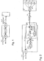
- Fig. 1
- mit wenigen Darstellungselementen einen Grundaufbau einer Anordnung aus Prozessor und externem Speicher und
- Fig. 2
- ein bevorzugtes Ausführungsbeispiel eines Prozessors mit einem externen Speicher und einer Codiereinrichtung zum Codieren von Daten, die zwischen dem Prozessor und dem externen Speicher zu übertragen sind.
Claims (12)
- Prozessor (P) mitgekennzeichnet durcheinem Prozessorkern (PC) zum Verarbeiten von Daten (d) undeiner Speicherschnittstelle (MIF) zum Übertragen der Daten (d) zwischen dem Prozessor (P) und einem externen Speicher (M) ,eine Codiereinrichtung (EC/DC) innerhalb oder an einer Schnittstelle des (P) zum Codieren und/oder Decodieren der über die Speicherschnittstelle (MIF) zu übertragenden bzw. übertragenen Daten (d) als codierte Daten(cd).
- Prozessor (P) nach Anspruch 1, bei dem die Codiereinrichtung (EC/DC) als fest im Prozessor (P) integrierter baulicher Bestandteil des Prozessors (P) ausgebildet ist.
- Prozessor (P) nach Anspruch 1 oder 2, bei dem eine Prozessorschnittstelle (PIF) als Ein- und/oder Ausgangsschnittstelle (PIF) über den Prozessorkern (PC) mit der Speicherschnittstelle (MIF) zum Übertragen codierter Daten (cd) von bzw. zum Speicher (M) verbunden ist (L1, L2, L3).
- Prozessor (P) nach Anspruch 3, bei dem die Prozessorschnittstelle (PIF) zum Übertragen uncodierter Daten (d) von bzw. zum Speicher (M) zusätzlich direkt mit der Speicherschnittstelle (MIF) verbunden ist (L5).
- Prozessor (P) nach einem vorstehenden Anspruch mit einer Leiteinrichtung (SW) zum wahlweisen Leiten der zwischen dem Prozessor (P) und dem Speicher (M) zu übertragenden Daten (d) als codierte Daten (cd) oder uncodierte Daten (d).
- Prozessor (P) nach Anspruch 5, bei dem die Leiteinrichtung (SW) die Daten (d) zum Codieren bzw. Decodieren durch die Codiereinrichtung (EC/DC) hindurch oder uncodiert an der Codiereinrichtung vorbeileitet.
- Prozessor (P) nach einem vorstehenden Anspruch, bei dem die Codiereinrichtung (EC/DC) zum Codieren der Daten (d) mit fallweise verschiedenen Codes ausgebildet ist.
- Prozessor (P) nach einem vorstehenden Anspruch mit einer Codierungsbestimmungseinrichtung (ADR) zum Festlegen einer zum Codieren bzw. Decodieren der Daten (d, cd) zu verwendenden Codierung bzw. Decodierung, die abhängig von den Daten (d, cd) oder von Datenzusatzinformationen aus einer Vielzahl verwendbaren Codierungen bzw. Decodierungen ausgewählt wird.
- Prozessor (P) nach Anspruch 8 mit einer Adressanalyseeinrichtung (ADR) als Codierungsbestimmungseinrichtung zum Analysieren einer den Daten (d, cd) zugeordneten Speicheradresse (MU, MA, MB, MC) und zum Bestimmen einer zum Codieren bzw. Decodieren der Daten (d, cd) zu verwendenden Codierung.
- Prozessor-Speicherschnittstelle (MIF) zum Aufbauen einer Verbindung eines Prozessors (P) und eines externen Speichers (M) nach einem vorstehenden Anspruch.
- Externer Speicher (M) zum Speichern von Daten (d, cd) eines Prozessors (P) nach einem vorstehenden Anspruch mitverschiedenen Speicherbereichen und/oder Adressbereichen (MU, MA, MB, MC) für unterschiedlich codierte Daten (d, cd) undeiner Speichersteuereinrichtung (MC) zum Zuordnen empfangener Daten (d, cd) zu den verschiedenen Speicherbereichen und/oder Adressbereichen abhängig von der verwendeten Codierung.
- Verfahren zum Speichern von Daten (d) eines Prozessors (P) in einem dem Prozessor (P) zugeordneten externen Speicher (M), bei demdadurch gekennzeichnet, dass die Daten (d) mit einem innerhalb des Prozessors (P) befindlichen Code codiert bzw. decodiert werden und als codierte Daten (CD) über die Speicherschnittstelle (MIF) übertragen werden.die Daten (d, cd) über eine Speicherschnittstelle (MIF) des Prozessors (P) zwischen dem Prozessor (P) und dem Speicher (M) übertragen werden,
Applications Claiming Priority (2)
| Application Number | Priority Date | Filing Date | Title |
|---|---|---|---|
| DE10306844 | 2003-02-18 | ||
| DE2003106844 DE10306844A1 (de) | 2003-02-18 | 2003-02-18 | Prozessor mit einem externen Speicher |
Publications (2)
| Publication Number | Publication Date |
|---|---|
| EP1482392A2 true EP1482392A2 (de) | 2004-12-01 |
| EP1482392A3 EP1482392A3 (de) | 2005-08-03 |
Family
ID=32797501
Family Applications (1)
| Application Number | Title | Priority Date | Filing Date |
|---|---|---|---|
| EP04002011A Withdrawn EP1482392A3 (de) | 2003-02-18 | 2004-01-30 | Prozessor mit einem externen Speicher |
Country Status (4)
| Country | Link |
|---|---|
| EP (1) | EP1482392A3 (de) |
| JP (1) | JP2004252978A (de) |
| KR (1) | KR20040074944A (de) |
| DE (1) | DE10306844A1 (de) |
Family Cites Families (11)
| Publication number | Priority date | Publication date | Assignee | Title |
|---|---|---|---|---|
| JPS63184853A (ja) * | 1987-01-28 | 1988-07-30 | Toshiba Corp | 携帯可能電子装置 |
| JPS6421637A (en) * | 1987-07-17 | 1989-01-25 | Fujitsu Ltd | Communication system between microprocessor and memory or peripheral lsi |
| US5130792A (en) * | 1990-02-01 | 1992-07-14 | Usa Video Inc. | Store and forward video system |
| US5224166A (en) * | 1992-08-11 | 1993-06-29 | International Business Machines Corporation | System for seamless processing of encrypted and non-encrypted data and instructions |
| US5892826A (en) * | 1996-01-30 | 1999-04-06 | Motorola, Inc. | Data processor with flexible data encryption |
| JP3747520B2 (ja) * | 1996-01-30 | 2006-02-22 | 富士ゼロックス株式会社 | 情報処理装置及び情報処理方法 |
| US5954817A (en) * | 1996-12-31 | 1999-09-21 | Motorola, Inc. | Apparatus and method for securing electronic information in a wireless communication device |
| US5987572A (en) * | 1997-09-29 | 1999-11-16 | Intel Corporation | Method and apparatus employing a dynamic encryption interface between a processor and a memory |
| JP2002529815A (ja) * | 1998-11-05 | 2002-09-10 | コーニンクレッカ フィリップス エレクトロニクス エヌ ヴィ | 複数の暗号化アルゴリズムを用いるセキュアメモリ管理ユニット |
| DE19858782A1 (de) * | 1998-12-18 | 2000-12-28 | Comtes Ges Fuer Computertechni | Schaltungsanordnung |
| WO2000057290A1 (en) * | 1999-03-19 | 2000-09-28 | Hitachi, Ltd. | Information processor |
-
2003
- 2003-02-18 DE DE2003106844 patent/DE10306844A1/de not_active Withdrawn
-
2004
- 2004-01-30 EP EP04002011A patent/EP1482392A3/de not_active Withdrawn
- 2004-02-17 KR KR1020040010227A patent/KR20040074944A/ko not_active Ceased
- 2004-02-17 JP JP2004039672A patent/JP2004252978A/ja active Pending
Also Published As
| Publication number | Publication date |
|---|---|
| JP2004252978A (ja) | 2004-09-09 |
| KR20040074944A (ko) | 2004-08-26 |
| EP1482392A3 (de) | 2005-08-03 |
| DE10306844A1 (de) | 2004-09-02 |
Similar Documents
| Publication | Publication Date | Title |
|---|---|---|
| DE4204119C2 (de) | Multiprozessorsystem | |
| EP1246043B1 (de) | Verfahren zur Übertragung von Daten über einen Datenbus | |
| DE19536169A1 (de) | Multifunktionale Chipkarte | |
| DE3102150A1 (de) | "schaltungsanordnung mit einem cachespeicher fuer eine zentraleinheit einer datenverarbeitungsanlage | |
| EP0049322A1 (de) | Auslesesicherung bei Einchip-Mikroprozessoren | |
| DE3432721A1 (de) | Datenschuetzender standard-mikroprozessor | |
| DE3046912C2 (de) | Schaltungsanordnung zum selektiven Löschen von Cachespeichern in einer Multiprozessor-Datenverarbeitungsanlage | |
| DE19860069B4 (de) | Programmierbare Steuereinrichtung | |
| DE19804784A1 (de) | Chipkarte mit integrierter Schaltung | |
| EP1482392A2 (de) | Prozessor mit einem externen Speicher | |
| DE3333894C2 (de) | ||
| WO2003027815A2 (de) | Programmgesteuerte einheit | |
| EP0097621A1 (de) | Verfahren zur Verschleierung digitaler Information und Vorrichtung zur Durchführung des Verfahrens | |
| DE10344636B4 (de) | Datenabhängige Ver/Entschlüsselung | |
| EP0890172B1 (de) | Halbleiterspeichervorrichtung | |
| EP2486489B1 (de) | Portabler datenträger mit zusatzfunktionalität | |
| DE3526130C2 (de) | ||
| DE2714314A1 (de) | Datenverarbeitende vorrichtung mit einem datenspeicher | |
| DE3335387A1 (de) | Verfahren zur verhinderung des ablaufs eines programms auf fuer den ablauf dieses programms nicht zugelassenen rechnern | |
| EP0331202B1 (de) | Verfahren zur bedarfsweisen Benutzung des Datenspeichers eines Mikrocomputers als Programmspeicher | |
| EP2219115B1 (de) | Verfahren zum Einsatz einer Multifunktionsspeicherkarte auf Endgeräten | |
| DE4028979C2 (de) | Einrichtung zur Diagnose von nicht rücklesbaren Ports in Mikrocomputern | |
| EP0994446B1 (de) | System zur Verarbeitung von Informationen und Informationsträger | |
| EP1899883B1 (de) | Verfahren zum schutz vertraulicher daten | |
| DE60029134T2 (de) | Verwaltung eines geheimschlüssels |
Legal Events
| Date | Code | Title | Description |
|---|---|---|---|
| PUAI | Public reference made under article 153(3) epc to a published international application that has entered the european phase |
Free format text: ORIGINAL CODE: 0009012 |
|
| AK | Designated contracting states |
Kind code of ref document: A2 Designated state(s): AT BE BG CH CY CZ DE DK EE ES FI FR GB GR HU IE IT LI LU MC NL PT RO SE SI SK TR |
|
| AX | Request for extension of the european patent |
Extension state: AL LT LV MK |
|
| PUAL | Search report despatched |
Free format text: ORIGINAL CODE: 0009013 |
|
| AK | Designated contracting states |
Kind code of ref document: A3 Designated state(s): AT BE BG CH CY CZ DE DK EE ES FI FR GB GR HU IE IT LI LU MC NL PT RO SE SI SK TR |
|
| AX | Request for extension of the european patent |
Extension state: AL LT LV MK |
|
| RIC1 | Information provided on ipc code assigned before grant |
Ipc: 7G 06F 12/14 B Ipc: 7G 06F 1/00 A |
|
| 17P | Request for examination filed |
Effective date: 20050913 |
|
| AKX | Designation fees paid |
Designated state(s): DE FR GB IT NL |
|
| 17Q | First examination report despatched |
Effective date: 20080110 |
|
| STAA | Information on the status of an ep patent application or granted ep patent |
Free format text: STATUS: THE APPLICATION HAS BEEN WITHDRAWN |
|
| 18W | Application withdrawn |
Effective date: 20120522 |