EP1478520B2 - Sicherheitsdokument und sicherheitselement für ein sicherheitsdokument - Google Patents
Sicherheitsdokument und sicherheitselement für ein sicherheitsdokument Download PDFInfo
- Publication number
- EP1478520B2 EP1478520B2 EP03742547.7A EP03742547A EP1478520B2 EP 1478520 B2 EP1478520 B2 EP 1478520B2 EP 03742547 A EP03742547 A EP 03742547A EP 1478520 B2 EP1478520 B2 EP 1478520B2
- Authority
- EP
- European Patent Office
- Prior art keywords
- security
- interference
- document
- layer
- security element
- Prior art date
- Legal status (The legal status is an assumption and is not a legal conclusion. Google has not performed a legal analysis and makes no representation as to the accuracy of the status listed.)
- Expired - Lifetime
Links
- 230000000694 effects Effects 0.000 claims abstract description 76
- 239000000758 substrate Substances 0.000 claims abstract description 42
- 238000012546 transfer Methods 0.000 claims abstract description 26
- 239000006096 absorbing agent Substances 0.000 claims description 33
- 239000011265 semifinished product Substances 0.000 claims description 19
- 239000000463 material Substances 0.000 claims description 15
- 229920003023 plastic Polymers 0.000 claims description 11
- 238000000034 method Methods 0.000 claims description 8
- 239000004033 plastic Substances 0.000 claims description 7
- 238000013461 design Methods 0.000 claims description 4
- 238000004519 manufacturing process Methods 0.000 claims 1
- 239000000047 product Substances 0.000 claims 1
- 238000010276 construction Methods 0.000 abstract 1
- 239000010410 layer Substances 0.000 description 127
- VYZAMTAEIAYCRO-UHFFFAOYSA-N Chromium Chemical compound [Cr] VYZAMTAEIAYCRO-UHFFFAOYSA-N 0.000 description 9
- 239000011241 protective layer Substances 0.000 description 7
- 230000005540 biological transmission Effects 0.000 description 5
- 229910052804 chromium Inorganic materials 0.000 description 5
- 239000011651 chromium Substances 0.000 description 5
- 238000000576 coating method Methods 0.000 description 5
- 230000003287 optical effect Effects 0.000 description 5
- VYPSYNLAJGMNEJ-UHFFFAOYSA-N Silicium dioxide Chemical compound O=[Si]=O VYPSYNLAJGMNEJ-UHFFFAOYSA-N 0.000 description 4
- 239000000853 adhesive Substances 0.000 description 4
- 230000001070 adhesive effect Effects 0.000 description 4
- 239000012790 adhesive layer Substances 0.000 description 4
- 239000011248 coating agent Substances 0.000 description 4
- 239000004922 lacquer Substances 0.000 description 4
- 239000002985 plastic film Substances 0.000 description 4
- 229910004298 SiO 2 Inorganic materials 0.000 description 3
- 150000001875 compounds Chemical class 0.000 description 3
- 238000004049 embossing Methods 0.000 description 3
- 230000001795 light effect Effects 0.000 description 3
- 238000007740 vapor deposition Methods 0.000 description 3
- XEEYBQQBJWHFJM-UHFFFAOYSA-N Iron Chemical compound [Fe] XEEYBQQBJWHFJM-UHFFFAOYSA-N 0.000 description 2
- UQSXHKLRYXJYBZ-UHFFFAOYSA-N Iron oxide Chemical compound [Fe]=O UQSXHKLRYXJYBZ-UHFFFAOYSA-N 0.000 description 2
- PXHVJJICTQNCMI-UHFFFAOYSA-N Nickel Chemical compound [Ni] PXHVJJICTQNCMI-UHFFFAOYSA-N 0.000 description 2
- KDLHZDBZIXYQEI-UHFFFAOYSA-N Palladium Chemical compound [Pd] KDLHZDBZIXYQEI-UHFFFAOYSA-N 0.000 description 2
- 229910010413 TiO 2 Inorganic materials 0.000 description 2
- 238000010521 absorption reaction Methods 0.000 description 2
- 229910052782 aluminium Inorganic materials 0.000 description 2
- XAGFODPZIPBFFR-UHFFFAOYSA-N aluminium Chemical compound [Al] XAGFODPZIPBFFR-UHFFFAOYSA-N 0.000 description 2
- 238000005229 chemical vapour deposition Methods 0.000 description 2
- 229910052681 coesite Inorganic materials 0.000 description 2
- 229910052906 cristobalite Inorganic materials 0.000 description 2
- 238000001704 evaporation Methods 0.000 description 2
- PCHJSUWPFVWCPO-UHFFFAOYSA-N gold Chemical compound [Au] PCHJSUWPFVWCPO-UHFFFAOYSA-N 0.000 description 2
- 229910052737 gold Inorganic materials 0.000 description 2
- 239000010931 gold Substances 0.000 description 2
- 238000010438 heat treatment Methods 0.000 description 2
- 229910052751 metal Inorganic materials 0.000 description 2
- 239000002184 metal Substances 0.000 description 2
- -1 metal fluorides Chemical compound 0.000 description 2
- 238000005240 physical vapour deposition Methods 0.000 description 2
- 229920006255 plastic film Polymers 0.000 description 2
- 239000000377 silicon dioxide Substances 0.000 description 2
- 238000004544 sputter deposition Methods 0.000 description 2
- 229910052682 stishovite Inorganic materials 0.000 description 2
- 229910052905 tridymite Inorganic materials 0.000 description 2
- 229910018072 Al 2 O 3 Inorganic materials 0.000 description 1
- OKTJSMMVPCPJKN-UHFFFAOYSA-N Carbon Chemical compound [C] OKTJSMMVPCPJKN-UHFFFAOYSA-N 0.000 description 1
- 239000004831 Hot glue Substances 0.000 description 1
- ZOKXTWBITQBERF-UHFFFAOYSA-N Molybdenum Chemical compound [Mo] ZOKXTWBITQBERF-UHFFFAOYSA-N 0.000 description 1
- RTAQQCXQSZGOHL-UHFFFAOYSA-N Titanium Chemical compound [Ti] RTAQQCXQSZGOHL-UHFFFAOYSA-N 0.000 description 1
- 229910052799 carbon Inorganic materials 0.000 description 1
- 239000011195 cermet Substances 0.000 description 1
- 238000006243 chemical reaction Methods 0.000 description 1
- BIJOYKCOMBZXAE-UHFFFAOYSA-N chromium iron nickel Chemical compound [Cr].[Fe].[Ni] BIJOYKCOMBZXAE-UHFFFAOYSA-N 0.000 description 1
- 229910017052 cobalt Inorganic materials 0.000 description 1
- 239000010941 cobalt Substances 0.000 description 1
- GUTLYIVDDKVIGB-UHFFFAOYSA-N cobalt atom Chemical compound [Co] GUTLYIVDDKVIGB-UHFFFAOYSA-N 0.000 description 1
- 230000001419 dependent effect Effects 0.000 description 1
- 238000011161 development Methods 0.000 description 1
- 230000018109 developmental process Effects 0.000 description 1
- 238000005566 electron beam evaporation Methods 0.000 description 1
- 230000008020 evaporation Effects 0.000 description 1
- 229920002457 flexible plastic Polymers 0.000 description 1
- 229910052732 germanium Inorganic materials 0.000 description 1
- GNPVGFCGXDBREM-UHFFFAOYSA-N germanium atom Chemical compound [Ge] GNPVGFCGXDBREM-UHFFFAOYSA-N 0.000 description 1
- 238000010348 incorporation Methods 0.000 description 1
- AMGQUBHHOARCQH-UHFFFAOYSA-N indium;oxotin Chemical class [In].[Sn]=O AMGQUBHHOARCQH-UHFFFAOYSA-N 0.000 description 1
- 230000006698 induction Effects 0.000 description 1
- 238000003780 insertion Methods 0.000 description 1
- 230000037431 insertion Effects 0.000 description 1
- 229910052742 iron Inorganic materials 0.000 description 1
- 238000000608 laser ablation Methods 0.000 description 1
- 150000001247 metal acetylides Chemical class 0.000 description 1
- 150000002736 metal compounds Chemical class 0.000 description 1
- 229910001512 metal fluoride Inorganic materials 0.000 description 1
- 150000002739 metals Chemical class 0.000 description 1
- 229910052750 molybdenum Inorganic materials 0.000 description 1
- 239000011733 molybdenum Substances 0.000 description 1
- 229910052759 nickel Inorganic materials 0.000 description 1
- 229910052758 niobium Inorganic materials 0.000 description 1
- 239000010955 niobium Substances 0.000 description 1
- GUCVJGMIXFAOAE-UHFFFAOYSA-N niobium atom Chemical compound [Nb] GUCVJGMIXFAOAE-UHFFFAOYSA-N 0.000 description 1
- 150000004767 nitrides Chemical class 0.000 description 1
- 229910052763 palladium Inorganic materials 0.000 description 1
- 230000000284 resting effect Effects 0.000 description 1
- 150000003346 selenoethers Chemical class 0.000 description 1
- 229910021332 silicide Inorganic materials 0.000 description 1
- 229910052950 sphalerite Inorganic materials 0.000 description 1
- 238000010025 steaming Methods 0.000 description 1
- 238000003860 storage Methods 0.000 description 1
- 150000003568 thioethers Chemical class 0.000 description 1
- 239000010936 titanium Substances 0.000 description 1
- 229910052719 titanium Inorganic materials 0.000 description 1
- 239000012780 transparent material Substances 0.000 description 1
- WFKWXMTUELFFGS-UHFFFAOYSA-N tungsten Chemical compound [W] WFKWXMTUELFFGS-UHFFFAOYSA-N 0.000 description 1
- 229910052721 tungsten Inorganic materials 0.000 description 1
- 239000010937 tungsten Substances 0.000 description 1
- 229910052720 vanadium Inorganic materials 0.000 description 1
- GPPXJZIENCGNKB-UHFFFAOYSA-N vanadium Chemical compound [V]#[V] GPPXJZIENCGNKB-UHFFFAOYSA-N 0.000 description 1
- 238000005019 vapor deposition process Methods 0.000 description 1
- 239000002966 varnish Substances 0.000 description 1
- 230000000007 visual effect Effects 0.000 description 1
- 229910052984 zinc sulfide Inorganic materials 0.000 description 1
Images

Classifications
-
- B—PERFORMING OPERATIONS; TRANSPORTING
- B42—BOOKBINDING; ALBUMS; FILES; SPECIAL PRINTED MATTER
- B42D—BOOKS; BOOK COVERS; LOOSE LEAVES; PRINTED MATTER CHARACTERISED BY IDENTIFICATION OR SECURITY FEATURES; PRINTED MATTER OF SPECIAL FORMAT OR STYLE NOT OTHERWISE PROVIDED FOR; DEVICES FOR USE THEREWITH AND NOT OTHERWISE PROVIDED FOR; MOVABLE-STRIP WRITING OR READING APPARATUS
- B42D25/00—Information-bearing cards or sheet-like structures characterised by identification or security features; Manufacture thereof
- B42D25/20—Information-bearing cards or sheet-like structures characterised by identification or security features; Manufacture thereof characterised by a particular use or purpose
- B42D25/29—Securities; Bank notes
-
- B—PERFORMING OPERATIONS; TRANSPORTING
- B42—BOOKBINDING; ALBUMS; FILES; SPECIAL PRINTED MATTER
- B42D—BOOKS; BOOK COVERS; LOOSE LEAVES; PRINTED MATTER CHARACTERISED BY IDENTIFICATION OR SECURITY FEATURES; PRINTED MATTER OF SPECIAL FORMAT OR STYLE NOT OTHERWISE PROVIDED FOR; DEVICES FOR USE THEREWITH AND NOT OTHERWISE PROVIDED FOR; MOVABLE-STRIP WRITING OR READING APPARATUS
- B42D25/00—Information-bearing cards or sheet-like structures characterised by identification or security features; Manufacture thereof
- B42D25/30—Identification or security features, e.g. for preventing forgery
- B42D25/324—Reliefs
-
- B—PERFORMING OPERATIONS; TRANSPORTING
- B42—BOOKBINDING; ALBUMS; FILES; SPECIAL PRINTED MATTER
- B42D—BOOKS; BOOK COVERS; LOOSE LEAVES; PRINTED MATTER CHARACTERISED BY IDENTIFICATION OR SECURITY FEATURES; PRINTED MATTER OF SPECIAL FORMAT OR STYLE NOT OTHERWISE PROVIDED FOR; DEVICES FOR USE THEREWITH AND NOT OTHERWISE PROVIDED FOR; MOVABLE-STRIP WRITING OR READING APPARATUS
- B42D25/00—Information-bearing cards or sheet-like structures characterised by identification or security features; Manufacture thereof
- B42D25/30—Identification or security features, e.g. for preventing forgery
- B42D25/328—Diffraction gratings; Holograms
-
- B—PERFORMING OPERATIONS; TRANSPORTING
- B42—BOOKBINDING; ALBUMS; FILES; SPECIAL PRINTED MATTER
- B42D—BOOKS; BOOK COVERS; LOOSE LEAVES; PRINTED MATTER CHARACTERISED BY IDENTIFICATION OR SECURITY FEATURES; PRINTED MATTER OF SPECIAL FORMAT OR STYLE NOT OTHERWISE PROVIDED FOR; DEVICES FOR USE THEREWITH AND NOT OTHERWISE PROVIDED FOR; MOVABLE-STRIP WRITING OR READING APPARATUS
- B42D25/00—Information-bearing cards or sheet-like structures characterised by identification or security features; Manufacture thereof
- B42D25/30—Identification or security features, e.g. for preventing forgery
- B42D25/351—Translucent or partly translucent parts, e.g. windows
-
- B—PERFORMING OPERATIONS; TRANSPORTING
- B42—BOOKBINDING; ALBUMS; FILES; SPECIAL PRINTED MATTER
- B42D—BOOKS; BOOK COVERS; LOOSE LEAVES; PRINTED MATTER CHARACTERISED BY IDENTIFICATION OR SECURITY FEATURES; PRINTED MATTER OF SPECIAL FORMAT OR STYLE NOT OTHERWISE PROVIDED FOR; DEVICES FOR USE THEREWITH AND NOT OTHERWISE PROVIDED FOR; MOVABLE-STRIP WRITING OR READING APPARATUS
- B42D25/00—Information-bearing cards or sheet-like structures characterised by identification or security features; Manufacture thereof
- B42D25/30—Identification or security features, e.g. for preventing forgery
- B42D25/355—Security threads
-
- B—PERFORMING OPERATIONS; TRANSPORTING
- B42—BOOKBINDING; ALBUMS; FILES; SPECIAL PRINTED MATTER
- B42D—BOOKS; BOOK COVERS; LOOSE LEAVES; PRINTED MATTER CHARACTERISED BY IDENTIFICATION OR SECURITY FEATURES; PRINTED MATTER OF SPECIAL FORMAT OR STYLE NOT OTHERWISE PROVIDED FOR; DEVICES FOR USE THEREWITH AND NOT OTHERWISE PROVIDED FOR; MOVABLE-STRIP WRITING OR READING APPARATUS
- B42D25/00—Information-bearing cards or sheet-like structures characterised by identification or security features; Manufacture thereof
- B42D25/30—Identification or security features, e.g. for preventing forgery
- B42D25/36—Identification or security features, e.g. for preventing forgery comprising special materials
-
- G—PHYSICS
- G03—PHOTOGRAPHY; CINEMATOGRAPHY; ANALOGOUS TECHNIQUES USING WAVES OTHER THAN OPTICAL WAVES; ELECTROGRAPHY; HOLOGRAPHY
- G03H—HOLOGRAPHIC PROCESSES OR APPARATUS
- G03H1/00—Holographic processes or apparatus using light, infrared or ultraviolet waves for obtaining holograms or for obtaining an image from them; Details peculiar thereto
- G03H1/02—Details of features involved during the holographic process; Replication of holograms without interference recording
- G03H1/0252—Laminate comprising a hologram layer
- G03H1/0256—Laminate comprising a hologram layer having specific functional layer
-
- G—PHYSICS
- G03—PHOTOGRAPHY; CINEMATOGRAPHY; ANALOGOUS TECHNIQUES USING WAVES OTHER THAN OPTICAL WAVES; ELECTROGRAPHY; HOLOGRAPHY
- G03H—HOLOGRAPHIC PROCESSES OR APPARATUS
- G03H2240/00—Hologram nature or properties
- G03H2240/50—Parameters or numerical values associated with holography, e.g. peel strength
- G03H2240/54—Refractive index
-
- G—PHYSICS
- G03—PHOTOGRAPHY; CINEMATOGRAPHY; ANALOGOUS TECHNIQUES USING WAVES OTHER THAN OPTICAL WAVES; ELECTROGRAPHY; HOLOGRAPHY
- G03H—HOLOGRAPHIC PROCESSES OR APPARATUS
- G03H2250/00—Laminate comprising a hologram layer
- G03H2250/36—Conform enhancement layer
Definitions
- the invention relates to a security element and a security document, in particular security, such as a banknote, with such a security element.
- security such as a banknote
- the invention equally relates to a semi-finished product for producing such a security document.
- the invention relates to a security element in the form of a security thread for incorporation into the security document as so-called window thread and in the form of a label or transfer element for application to the security document.
- Security documents for the purposes of the present invention are in particular banknotes, but also checks, check cards, credit cards, identity cards, passports, entrance tickets, tickets and the like.
- semi-finished products for producing the aforementioned security documents for example, unprinted security paper and other unprinted security document substrates come into consideration.
- the aforementioned security documents are usually equipped by means of embedded security threads or applied security labels or transfer elements for protection against counterfeiting and as a proof of authenticity.
- Security threads in the form of window threads are widely known, for example, in connection with value documents, such as banknotes, but are also generally suitable for use in check cards and the like.
- Window threads are embedded in the base material of the security document and appear periodically on the security document surface so that they are visually recognizable in these "window areas". In translucent substrates results in a so-called reflected light / transmitted light effect, the security thread viewed in transmitted light appears to the surrounding material as a dark stripe. In contrast, the security thread is only visible in the window areas in incident light.
- a see-through window thread spans, so to speak, a hole or a transparent area in the value document.
- Another two-sided window thread is the security thread referred to below as an alternating window thread, which is alternately visible on the front and back of a document.
- transfer elements these usually having recesses, e.g. a hole, span in a document.
- the security elements have complex, visually and / or mechanically verifiable security features that are imitable only with great effort. In order to additionally increase counterfeit protection, such security elements often have several different security features, which in their combination can also have a new common effect.
- a security feature frequently encountered in security elements is a multilayer dichroic coating whose color impression changes depending on the viewing angle and / or depending on the viewing in transmitted light or incident light. This phenomenon is due to interference effects due to the superposition of multiple reflections and / or transmissions of light waves within the layer structure in combination with selective absorption properties of the layer materials.
- the color change with varying viewing angle is also referred to as color shift effect or color shift effect.
- the color change with changing observation in reflected light and in transmitted light is referred to below as the color change effect.
- Optical interference coatings with color shift effect are described in connection with security elements, for example in EP 0 341 002 B1 and US 3,858,977 , Depending on the type and number of layers in the layer structure, 2, 3, 4 or more different color effects depending on the viewing angle may occur.
- the reflection and transmission properties of such color shift effect layers depend on several factors, in particular the refractive indices, absorption coefficients and layer thicknesses and the number of layers of the layer structure.
- the object of the present invention is therefore to provide security elements, in particular a security thread or a transfer element, which have an increased security against forgery compared to the prior art.
- the security element comprises a multi-layered interference element that produces a color shift effect on both the front and the back of the security element when the security element is viewed at different angles.
- the color shift effect can be the same on the front and back of the security element, but also designed differently.
- the security element has diffractive structures that interfere with the Interference element at least partially overlay.
- the interference element is formed by superimposed interference layers, the absorber and dielectric layers, wherein a plurality of absorber and dielectric layers can be arranged alternately one above the other.
- alternating absorber and dielectric layers it is also possible to provide exclusively dielectric layers, wherein adjoining layers have very different refractive indices, so that a color-shift effect is produced.
- the use of the absorber layers is advantageous because the color shift effects are more visible.
- the interference element I may have a multilayer structure, but preferably comprises at least three interference layers, namely two absorber layers A 1 , A 2 and a dielectric layer D lying between the absorber layers.
- Such a three-layer interference element can exhibit a dichroic color shift effect at changing viewing angles and / or when changing between Incident light and transmitted light observation cause.
- further dielectric and / or absorber layers in an alternating sequence further color changes can be achieved or color changes can be intensified.
- absorber layers A 1 , A 2 are typically metal layers of materials such as chromium, iron, gold, aluminum or titanium in a thickness of preferably 4 nm to 20 nm.
- absorber layer materials and compounds such as nickel-chromium-iron or more rare metals such as vanadium, Palladium or molybdenum can be used.
- Other suitable materials include nickel, cobalt, tungsten, niobium, aluminum, metal compounds such as metal fluorides, oxides, sulfides, nitrides, carbides, phosphides, selenides, silicides and compounds thereof, as well as carbon, germanium, Cermet, iron oxide and the like.
- the absorber layers may be identical, but may also be different in thickness and / or consist of different materials.
- the dielectric layer are mainly transparent materials with a low refractive index ⁇ 1.7 into consideration, such as SiO 2 MgF, SiO x with 1 ⁇ x ⁇ 2 and Al 2 O 3 .
- transparent materials with a low refractive index ⁇ 1.7 into consideration, such as SiO 2 MgF, SiO x with 1 ⁇ x ⁇ 2 and Al 2 O 3 .
- almost all vapor-deposited, transparent compounds are suitable, in particular also higher-refractive coating materials, such as ZrO 2 ZnS, TiO 2 and indium tin oxides (ITO).
- the layer thickness of the dielectric layer D is in the range of 100 nm to 1000 nm, preferably 200 nm to 500 nm.
- the absorber and the dielectric layers of the interference element I are produced in the Vakuumbedampfungs vide on the substrate S, which may form part of the security element 1, but which can also serve only as an intermediate carrier and is removed at the latest when applying the security element on or in an object.
- a methodological group is Physical Vapor Deposition (PVD) with Schiffchenbedampfung, evaporation by resistance heating, vapor deposition by induction heating or electron beam evaporation, sputtering (DC or AC) and arc vapor deposition.
- PVD Physical Vapor Deposition
- the vapor deposition can also be carried out as a chemical vapor deposition (CVD) such. Sputtering in the reactive plasma or any other plasma-assisted evaporation method.
- the structure of the interference element can be chosen so that the color game is the same or different depending on the viewing side of the security element.
- the interference element is symmetrical, i. On the front and back of the security element, the viewer perceives the same color-shift effect. Different effects arise, for example, by varying the materials used in individual layers and / or by varying the layer thicknesses of the individual layers constituting the interference element.
- the interference element is configured semitransparent.
- semitransparency translucency, i. the layer has a light transmission of less than 90%, preferably between 80% and 20%.
- Refraction patterns, transmission, volume or reflection holograms, but also lattice structures, which are preferably part of the substrate carrying the interference element, but which can also be incorporated in any other suitable layer or in an additional layer, may be considered as diffraction structures.
- the additional layer may be e.g. to act a varnish layer.
- the diffraction structures are preferably introduced into the surface of a transparent plastic substrate forming the security element, in particular embossed.
- the interference element is on the side of the plastic substrate, in which the relief structure is imprinted.
- the interference layers are then applied to the plastic substrate, in particular vapor-deposited in vacuo.
- the embossing of the plastic substrate can also take place after the vapor deposition process. This results in several variants that have different visual effects and therefore may be more or less preferred depending on the purpose.
- the diffraction structures are formed by a relief pattern which directly adjoins the interference layer. Because then the diffraction effects of each page of the security element are almost equally recognizable. If the security element is stored as a two-sided window thread in a document, the diffraction effect is visible from both sides. The same applies to the application of the security element in front of a hole or as a see-through window thread when such a document is viewed in reflected light, for example on a base.
- the optical effect of such a security element is essentially determined by the color effect of the interference element from both viewing sides.
- the diffraction structures determine the optical appearance substantially at least from one viewing side, with a suitable layer structure also from both viewing sides. In this case, the effects of both security features overlap.
- the diffraction effects appear optically especially when viewed in incident light, e.g. if the document is lying on a surface. When viewed in transmitted light, the diffraction effects are significantly reduced. The color shift effect is pronounced in reflected light as in transmitted light.
- Such a security element is particularly suitable for covering e.g. printed information on an object that should only be recognizable from a certain viewing angle.
- Information printed in gold for example, is recognizable only at the second viewing angle in the case of a security element which appears green under a first viewing angle and appears golden under a second viewing angle. With a suitable color choice of the color shift effect and the information, these are thus clearly perceptible at certain viewing angles, but almost invisible under other viewing angles.
- Such a security element is particularly suitable for use as a two-sided security thread, since it can be seen from each viewing page particularly characteristic security features that are visually verifiable.
- a two-sided security thread can be used either as an alternating security thread that appears at different points of the security document on the opposite security document surfaces or at least visible. However, it can also be used as a see-through window thread, where it is visually recognizable from both sides of the document in a particularly thin or transparent area of the document, or where it spans a hole in the document.
- such a security element is also suitable as a transfer element, e.g. in the form of a label or patch applied over a hole on a surface of the security document. Viewed from one side of the document, it gives the impression of a patch with a color shift effect. Seen from the other side, you can see through the hole of the document a section of the patch with a different or possibly an identical color shift effect, it depends on the specific layer structure of the security element, whether a possibly existing diffraction design from both sides or only from one side is recognizable from.
- a "transfer element" in the sense of the invention is a security element which is prepared on a separate carrier layer, for example a plastic film, in the reverse order as it later comes to lie on the security paper and then into the surface by means of an adhesive or lacquer layer desired outlines is transferred to the security paper.
- the form of the security element is not limited and it is conceivable all possible outline shapes to filigree structures, such as guilloches, etc. Frequently, the security elements are also formed in the form of strips which run parallel to the edge of the value document.
- the carrier layer can be removed after the transfer of the layer structure of the security element or remain as a protective layer as an integral part of the security element on the layer structure.
- the individual transfer elements can be prepared on the carrier layer as separate individual elements in the outline shapes to be transferred.
- the layer sequence of the transfer elements is provided in continuous form on the carrier layer.
- Such carrier layers with spaced individual transfer elements or a continuously extending layer structure are hereinafter referred to as "transfer material” and arranged on the carrier layer layer sequence of the security element as a "transfer layer”.
- the transfer material is then connected to the security paper via an adhesive layer and the adhesive layer is activated via corresponding embossing tools so that the transfer layer adheres to the security paper only in the activated areas. All other areas are then removed with the carrier layer.
- the adhesive layer can also be designed in the form of the security element to be transferred.
- adhesives hot melt adhesives are preferably used. However, it is also possible to use any other adhesives, such as reaction lacquers.
- the security element constructed according to the invention can be combined with further security features, in particular with a negative or positive writing by local removal of one of the interference layers of the interference element.
- the multi-layer interference element according to the invention only one layer is locally removed.
- the recesses are preferably located in the first or second absorber layer.
- the font is preferably alphanumeric characters, but is not limited thereto. For the purposes of the invention may be any representable pattern, characters or coding. Due to the recesses in the layer structure, this results in an additional reflected light / transmitted light effect.
- the characters, patterns and encodings of such stored in a document of value security element are barely perceptible in reflected light, but when viewed in transmitted light clearly appear as lighter areas against a dark environment. Depending on which layers are locally removed in the interference element, also color effects in the transmitted and transmitted light can be controlled.
- FIG. 1 shows a security document 1, for example, a banknote made of paper or a passport card made of plastic, which is equipped with two security elements 2, 4.
- the first security element 2 is a patch which is applied to a surface of the document 1 as a label or transfer element over a hole or other transparent area 3 of the document 1, for example by means of an adhesive.
- the second security element 4 is a two-sided window security thread, which is incorporated in the document 1 either alternately or as a see-through window thread.
- FIGS. 2 to 4 the different types of application and storage of the security elements 2 and 4 are shown by way of example.
- FIG. 2 shows the security document 1 FIG. 1 in cross section along the line II - II through the patch.
- the hole can e.g. already made paper-making in papermaking or subsequently stamped into the paper.
- the imprint can be concealed under the patch 2 at a certain viewing angle, but visible at a different angle.
- the patch 2 in the area of the hole 3 can be seen from both sides.
- FIG. 3 displays the window security thread FIG. 1 as a see-through window thread.
- the document for example a banknote
- the document 1 has window areas 6 which are designed to be very thin and in extreme cases as a hole, so that the security thread 4 is visible from both sides of the document 1.
- the optical effect of the security thread 4 in reflected light and transmitted light then corresponds to the appearance of in relation to FIG. 2
- the patch window areas 6 have the same function as the hole 3.
- the security thread can also be stored as an alternating two-sided window security thread in a document (not shown).
- the thread runs through windows alternately on one side and on the other side of the document. Regardless of the viewing page of the document, the color shift effect is then recognizable in the window areas.
- such a security thread 4 can also be used as a simple window security thread, which, as in FIG. 4 shown, only one side in windows 7 comes to light.
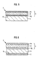
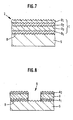
- FIGS. 5 to 8 are different layer structures of a security element 2 and 4 partially in cross section.
- both security elements are multilayered and have a Farbkipp bin generating interference element, which is superimposed with diffraction structures. Accordingly, the interference element and the diffractive structures have an influence on the appearance of the security element for each of its viewing sides. Depending on the design of the layer structure, the appearance of the security element may be the same on both sides, but also different depending on the viewing side.
- FIG. 5 shows a fragmentary cross-section of the layer structure of a security element 2.
- the security element 4 may be constructed accordingly.
- a transparent substrate S preferably a plastic film, has on one side an embossed holographic surface relief 8, which is superimposed directly by an interference element I.
- the surface relief 8 can also be embossed in an additional lacquer layer, wherein the lacquer layer can be present on one of the two substrate sides or on the outer side of the absorber layer A 1 .
- the interference element I consisting of two absorber and one dielectric layer, has a dichroic color shift effect at different viewing angles, for example a change between green and magenta.
- the security element on the front and back has the same color shift effect. Any further interference layers and / or transparent layers may be provided over the interference element I.
- the diffraction-optical effect of a security element with a layer structure according to FIG. 5 is clearly visible in reflected light from every viewing page. In transmitted light, the diffraction-optical effects almost completely disappear. The color shift effect can be seen on both sides of the security element both in reflected light and transmitted light.
- the interference layers each have only one layer thickness of less than 1 ⁇ m (the figures represent the layer structure only schematically), all layers have the same relief pattern as the relief structure 8 on which the layers are vapor-deposited. This has the consequence that the holographic effects caused by the relief structure 8 can be recognized from both viewing sides.
- the interference element is symmetrical, such a security element can be used particularly well as a two-sided security thread, because the diffractive effect and the color shift effect are almost identical on both sides. When storing the security thread therefore does not need to be paid to sidelongness.
- FIG. 6 a not belonging to the invention alternative layer structure of the security element 2 is shown.
- the surface relief 8 is stamped on the side of the substrate S facing away from the interference element I into the substrate surface.
- An optional protective layer C covers the sensitive relief structure 8.
- the refractive index of the protective layer C differs substantially from the refractive index of the substrate S, so that the diffraction-optical effect produced by the relief structure is as pronounced as possible.
- the protective layer may also be a two-layer system.
- a highly refractive layer for example made of TiO 2 , ZnS, ZrO 2 or the like, can be vapor-deposited onto the relief structure 8, to which a protective layer is applied. In this case, no special requirements are to be met for the refractive index of the protective layer.
- a color shift effect is perceptible. Holographic effects do not occur on this viewing page. If the same security element is viewed from the opposite side, ie from the substrate side, then a diffraction-optical effect produced by the diffraction structure 8 and the color-shift effect are perceptible. Overall results in a layer structure according to FIG. 6 Thus, on one viewing side, a hologram effect combined with a color shift effect and on the other viewing side, a color shift effect without superimposed diffraction effects.
- the interference element I has a recess 9 which in FIG. 8 only in cross section can be seen.
- the recess 9 may take the form of characters, patterns or codes. These patterns, characters or codes appear optically particularly in transmitted light.
- the security element is transparent or at least semitransparent in the area of the recesses 9 and does not show any color shift effect or one of the areas surrounding the recesses. If the interference layers in the recesses completely removed, it can be achieved that the recesses in the transmitted light appear completely colorless. This results in an additional reflected light / transmitted light effect.
- the recesses 9 which may have the form of characters, patterns or codes, in the reflected light, depending on the design of the layer structure, less good or barely perceptible.
- the color shift effect is visible both from the substrate side and from the side opposite the substrate side.
- the recesses can be seen in transmitted light.
- the diffraction-optical effects due to the diffraction structures (8) are visible in incident light from both sides of the security element. In the areas of the recesses, the Colorshift effects are no longer recognizable.
- the recesses 9 in the interference element I can be generated by laser ablation on an intermediate carrier carrying the interference element I or else only on the substrate S.
- the substrate S can also be printed with a soluble color in the area of the recesses 9 before the interference layers are vapor-deposited, and in a subsequent process the soluble color with the overlying interference layers in the area of the recesses 9 can be dissolved out.
- the skilled person numerous other methods for producing the recesses 9 are known.
- interference layers in the recesses 9 are not completely removed, e.g. only recesses in one or both absorber layers before, can be dispensed with the additional presence of diffraction structures.
- the thus formed security element was applied to a banknote over a hole.
- the security element had a distinct color shift effect of green when viewed perpendicularly to magenta when viewed at an angle ⁇ 45 °.
- the security element When viewed in transmitted light, the security element is translucent and the color shift effect of both viewing pages clearly visible. The hologram effects almost completely disappeared when viewed in transmitted light.
- the hologram effect When viewed in incident light on a substrate, however, the hologram effect is clearly visible from both sides of the security element. The color shift effect is also clearly visible.
- the holographic effects in combination with the colored interference element gave an extraordinarily colored impression, in contrast to typical reflection holograms with a metallic background.
- the substrate S is preferably transparent, possibly colored transparent or colored transparent coated.
- the substrate S is preferably a flexible plastic film, which is cut into strips, threads or labels after the embossing of the relief structure 8 and after the coating with the interference element I.
- the substrate S can also be present on a transfer film and transferred to the document in the transfer process, for example in the hot-stamp process.
- the security element can either be adhesively attached to an article as a label after removal of the covering layer or transferred as a transfer element in the transfer process.
Landscapes
- Business, Economics & Management (AREA)
- Accounting & Taxation (AREA)
- Finance (AREA)
- Physics & Mathematics (AREA)
- General Physics & Mathematics (AREA)
- Credit Cards Or The Like (AREA)
- Laminated Bodies (AREA)
- Paper (AREA)
- Diffracting Gratings Or Hologram Optical Elements (AREA)
Applications Claiming Priority (3)
| Application Number | Priority Date | Filing Date | Title |
|---|---|---|---|
| DE10207622A DE10207622A1 (de) | 2002-02-22 | 2002-02-22 | Sicherheitsdokument und Sicherheitselement für ein Sicherheitsdokument |
| DE10207622 | 2002-02-22 | ||
| PCT/EP2003/001677 WO2003070482A1 (de) | 2002-02-22 | 2003-02-19 | Sicherheitsdokument und sicherheitselement für ein sicherheitsdokument |
Publications (3)
| Publication Number | Publication Date |
|---|---|
| EP1478520A1 EP1478520A1 (de) | 2004-11-24 |
| EP1478520B1 EP1478520B1 (de) | 2009-05-27 |
| EP1478520B2 true EP1478520B2 (de) | 2015-01-21 |
Family
ID=27674868
Family Applications (1)
| Application Number | Title | Priority Date | Filing Date |
|---|---|---|---|
| EP03742547.7A Expired - Lifetime EP1478520B2 (de) | 2002-02-22 | 2003-02-19 | Sicherheitsdokument und sicherheitselement für ein sicherheitsdokument |
Country Status (11)
| Country | Link |
|---|---|
| US (1) | US7611168B2 (enExample) |
| EP (1) | EP1478520B2 (enExample) |
| JP (1) | JP4308020B2 (enExample) |
| CN (1) | CN1628039B (enExample) |
| AT (1) | ATE432172T1 (enExample) |
| AU (1) | AU2003210307B2 (enExample) |
| CA (1) | CA2476882C (enExample) |
| DE (2) | DE10207622A1 (enExample) |
| RU (1) | RU2309853C2 (enExample) |
| UA (1) | UA83797C2 (enExample) |
| WO (1) | WO2003070482A1 (enExample) |
Families Citing this family (63)
| Publication number | Priority date | Publication date | Assignee | Title |
|---|---|---|---|---|
| DE10255639A1 (de) * | 2002-11-28 | 2004-06-17 | Giesecke & Devrient Gmbh | Sicherheitselement und Verfahren zur Herstellung desselben |
| DE10305288B4 (de) * | 2003-02-10 | 2005-06-30 | Leonhard Kurz Gmbh & Co. Kg | Sicherheitsdokument mit wenigstens einem Sicherheitselement |
| AT504587A1 (de) | 2004-02-16 | 2008-06-15 | Hueck Folien Gmbh | Fälschungssicheres sicherheitsmerkmal mit farbkippeffekt |
| DE102004014778A1 (de) * | 2004-03-26 | 2005-10-13 | Leonard Kurz Gmbh & Co. Kg | Sicherheits- und/oder Wertdokument |
| US20070211238A1 (en) * | 2004-04-30 | 2007-09-13 | Giesecke & Devrient Gmbh | Security Element and Methods for the Production Thereof |
| GB0409736D0 (en) * | 2004-04-30 | 2004-06-09 | Rue De Int Ltd | Improvements in substrates incorporating security device |
| DE102004027090A1 (de) * | 2004-06-03 | 2006-01-05 | Schott Ag | Verbundmaterial mit einem Dekor und einer Funktionsschicht sowie Verfahren zu desen Herstellung |
| FR2872322B1 (fr) * | 2004-06-23 | 2006-09-22 | Arjowiggins Security Soc Par A | Article tel qu'un support de donnees ou un dispositif de conditionnement, comportant une structure interferencielle multicouche semi-reflechissante |
| ES2428360T5 (es) * | 2004-08-12 | 2019-04-16 | Giesecke & Devrient Currency Technology Gmbh | Elemento de seguridad con soporte |
| DE102005022018A1 (de) * | 2005-05-12 | 2006-11-16 | Giesecke & Devrient Gmbh | Sicherheitspapier und Verfahren zu seiner Herstellung |
| DE102005027380B4 (de) * | 2005-06-14 | 2009-04-30 | Ovd Kinegram Ag | Sicherheitsdokument |
| GB0525886D0 (en) * | 2005-12-20 | 2006-02-01 | Rue De Int Ltd | Improvements in security substrates |
| GB2438383B (en) * | 2006-05-26 | 2008-10-08 | Rue De Int Ltd | Improvements in substrates |
| FR2904835B1 (fr) * | 2006-08-08 | 2010-03-19 | Arjowiggins | Elements de securite de format relativement petit comprenant un trou traversant et feuille les comprenant |
| JP5211474B2 (ja) * | 2006-11-30 | 2013-06-12 | 凸版印刷株式会社 | 積層体、粘着ラベル、記録媒体及びラベル付き物品 |
| JP5211473B2 (ja) * | 2006-11-30 | 2013-06-12 | 凸版印刷株式会社 | 積層体、粘着ラベル、記録媒体及びラベル付き物品 |
| DE102007039996B4 (de) | 2007-02-07 | 2020-09-24 | Leonhard Kurz Stiftung & Co. Kg | Sicherheitselement für ein Sicherheitsdokument und Verfahren zu seiner Herstellung |
| CN101269610B (zh) * | 2007-03-21 | 2012-06-27 | 中钞特种防伪科技有限公司 | 一种光学防伪元件及带有该防伪元件的产品 |
| DE102007062089A1 (de) * | 2007-12-21 | 2009-07-02 | Giesecke & Devrient Gmbh | Verfahren zum Erzeugen einer Mikrostruktur |
| DE102008009296A1 (de) * | 2008-02-15 | 2009-08-20 | Giesecke & Devrient Gmbh | Sicherheitselement und Verfahren zu seiner Herstellung |
| USD582977S1 (en) * | 2008-02-21 | 2008-12-16 | Jpmorgan Chase Bank, N.A. | Transaction device |
| DE102008013167A1 (de) * | 2008-03-07 | 2009-09-10 | Giesecke & Devrient Gmbh | Sicherheitselement und Verfahren zu seiner Herstellung |
| EP2271959A4 (en) * | 2008-05-06 | 2012-03-28 | Hewlett Packard Development Co | MANUFACTURE OF THIN PELLICULAR RADIATORS |
| DE102008030694A1 (de) | 2008-07-01 | 2010-01-07 | Giesecke & Devrient Gmbh | Verfahren zur Herstellung eines Sicherheitselements mit beidseitiger Extrusionsbeschichtung |
| DE102009008853A1 (de) | 2009-02-13 | 2010-08-19 | Giesecke & Devrient Gmbh | Durchsichtssicherheitselement |
| RU2406152C1 (ru) * | 2009-04-28 | 2010-12-10 | Общество С Ограниченной Ответственностью "Новые Энергетические Технологии" | Защитный элемент для проверки подлинности объекта защиты и способ проверки подлинности |
| DE102009036314A1 (de) * | 2009-08-06 | 2011-02-10 | Giesecke & Devrient Gmbh | Verfahren zur Herstellung eines Sicherheitselements und nach dem Verfahren erhältliches Sicherheitselement |
| DE102009041583A1 (de) * | 2009-09-15 | 2011-03-17 | Giesecke & Devrient Gmbh | Dünnschichtelement mit Interferenzschichtaufbau |
| DE102009058243A1 (de) * | 2009-12-14 | 2011-06-16 | Giesecke & Devrient Gmbh | Dünnschichtelement mit Mehrschichtstruktur |
| DE102010008874A1 (de) * | 2010-02-22 | 2011-08-25 | Giesecke & Devrient GmbH, 81677 | Sicherheitselement mit Volumenhologramm |
| DE102010009976A1 (de) | 2010-03-03 | 2011-09-08 | Giesecke & Devrient Gmbh | Wertdokument mit registergenau positioniertem Sicherheitselement |
| DE102010050895A1 (de) * | 2010-11-10 | 2012-05-10 | Giesecke & Devrient Gmbh | Dünnschichtelement mit Mehrschichtstruktur |
| EP2760680B2 (en) | 2011-09-26 | 2023-02-15 | Crane Security Technologies, Inc. | Method for producing a composite web and security devices prepared from the composite web |
| DE102011115133A1 (de) * | 2011-10-07 | 2013-04-11 | Giesecke & Devrient Gmbh | Verfahren und Vorrichtung zum Herstellen eines blattförmigen Substrates |
| DE102012204340A1 (de) * | 2012-03-19 | 2013-09-19 | Bundesdruckerei Gmbh | Sicherheitsdokument mit einem Perforationsfenster und Verfahren zu dessen Herstellung |
| DE102012015900A1 (de) | 2012-08-10 | 2014-03-06 | Giesecke & Devrient Gmbh | Sicherheitselement mit farbeffekterzeugendem Gitter |
| DE102012108169A1 (de) | 2012-09-03 | 2014-05-28 | Ovd Kinegram Ag | Sicherheitselement sowie Sicherheitsdokument |
| JP2013033263A (ja) * | 2012-09-13 | 2013-02-14 | Dainippon Printing Co Ltd | 偽造防止材及びこれを備えた印刷基材 |
| FR3004470B1 (fr) | 2013-04-11 | 2015-05-22 | Arjowiggins Security | Element de securite comportant un pigment interferentiel et une charge nanometrique. |
| FR3004471B1 (fr) | 2013-04-11 | 2015-10-23 | Arjowiggins Security | Element de securite comportant une structure de masquage contenant un melange de charges nanometriques. |
| GB201400910D0 (en) * | 2014-01-20 | 2014-03-05 | Rue De Int Ltd | Security elements and methods of their manufacture |
| GB201403988D0 (en) * | 2014-03-06 | 2014-04-23 | Rue De Int Ltd | Security documents and methods of manufacture thereof |
| US10490521B2 (en) * | 2014-06-26 | 2019-11-26 | Taiwan Semiconductor Manufacturing Company, Ltd. | Advanced structure for info wafer warpage reduction |
| WO2016075928A1 (ja) * | 2014-11-10 | 2016-05-19 | 凸版印刷株式会社 | 偽造防止用の光学素子 |
| DE102015014505A1 (de) * | 2015-11-10 | 2017-05-11 | Giesecke & Devrient Gmbh | Sicherheitselement, Verfahren zum Herstellen desselben und mit dem Sicherheitselement ausgestatteter Datenträger |
| DE102015015733A1 (de) * | 2015-12-01 | 2017-06-01 | Giesecke & Devrient Gmbh | Sicherheitselement und mit demselben ausgestatteter Datenträger |
| WO2017102722A1 (en) * | 2015-12-17 | 2017-06-22 | Sicpa Holding Sa | Security element formed from at least two inks applied in overlapping patterns, articles carrying the security element, and authentication methods |
| KR102642776B1 (ko) | 2016-02-09 | 2024-03-05 | 도판 홀딩스 가부시키가이샤 | 위조 방지용 광학 소자 및 정보 기록 매체 |
| AU2017245036B2 (en) | 2016-03-30 | 2019-06-13 | Toppan Printing Co., Ltd. | Counterfeit-preventive optical element and information medium |
| GB2555491B (en) | 2016-11-01 | 2019-03-27 | De La Rue Int Ltd | Security devices and methods of manufacture thereof |
| DE102016014230A1 (de) | 2016-11-30 | 2018-05-30 | Giesecke & Devrient Gmbh | Wertdokument, Verfahren zum Herstellen desselben und Wertdokumentsystem |
| DE102016014662A1 (de) | 2016-12-09 | 2018-06-14 | Giesecke+Devrient Currency Technology Gmbh | Wertdokument |
| WO2018169441A1 (en) * | 2017-03-11 | 2018-09-20 | Andrey Karasev | Security ovd |
| GB2567165B (en) * | 2017-10-04 | 2020-08-26 | De La Rue Int Ltd | Improvements in security sheets comprising security elements |
| GB2576218B (en) * | 2018-08-10 | 2021-09-15 | De La Rue Int Ltd | Security devices and methods of authentication thereof |
| CN111746171B (zh) * | 2019-03-29 | 2021-06-15 | 中钞特种防伪科技有限公司 | 光学防伪元件及其制作方法 |
| CN112339471B (zh) | 2019-08-09 | 2022-04-15 | 中钞特种防伪科技有限公司 | 光学防伪元件及光学防伪产品 |
| CN112389111A (zh) * | 2019-08-19 | 2021-02-23 | 中钞特种防伪科技有限公司 | 光学防伪元件及光学防伪产品 |
| EP3800062A1 (de) * | 2019-10-03 | 2021-04-07 | Hueck Folien Gesellschaft m.b.H. | Sicherheitselement mit einer als dünnschichtelement ausgebildeten optischen effektschicht |
| EP3800060A1 (de) | 2019-10-03 | 2021-04-07 | Hueck Folien Gesellschaft m.b.H. | Sicherheitselement mit zumindest einem ersten farbkippenden bereich |
| EP3800061A1 (de) * | 2019-10-03 | 2021-04-07 | Hueck Folien Gesellschaft m.b.H. | Sicherheitselement mit einer optischen effektschicht |
| CN111016494B (zh) * | 2019-11-20 | 2021-01-26 | 中钞特种防伪科技有限公司 | 防伪元件及防伪产品 |
| JP6971511B1 (ja) * | 2021-06-01 | 2021-11-24 | 株式会社ユーロックテクノパーツ | レーザ刻印シール |
Citations (5)
| Publication number | Priority date | Publication date | Assignee | Title |
|---|---|---|---|---|
| CA2569243A1 (en) † | 1993-05-01 | 1994-11-02 | Giesecke & Devrient Gmbh | Antifalsification paper |
| EP0657297B1 (en) † | 1993-12-10 | 1997-07-30 | Agfa-Gevaert N.V. | Security document having a transparent or translucent support and containing interference pigments. |
| CA2163528C (en) † | 1993-10-13 | 1998-12-08 | Jurgen Herrmann | Value-bearing document with window |
| WO2000039391A1 (en) † | 1998-12-29 | 2000-07-06 | De La Rue International Limited | Improvements in making paper |
| WO2002000445A1 (en) † | 2000-06-28 | 2002-01-03 | De La Rue International Limited | Optically variable security device |
Family Cites Families (31)
| Publication number | Priority date | Publication date | Assignee | Title |
|---|---|---|---|---|
| US2388352A (en) * | 1942-04-27 | 1945-11-06 | Temp R Lens Corp | Comparing device |
| US3858977A (en) | 1972-01-18 | 1975-01-07 | Canadian Patents Dev | Optical interference authenticating means |
| GB1552853A (en) * | 1976-09-24 | 1979-09-19 | Bank Of England | Authentication devices |
| CH653161A5 (de) * | 1981-10-27 | 1985-12-13 | Landis & Gyr Ag | Dokument mit einem sicherheitsmerkmal und verfahren zur echtheitspruefung des dokumentes. |
| US4838648A (en) | 1988-05-03 | 1989-06-13 | Optical Coating Laboratory, Inc. | Thin film structure having magnetic and color shifting properties |
| DE3840729C2 (de) * | 1988-12-02 | 1997-07-17 | Gao Ges Automation Org | Mehrschichtiger Aufzeichnungsträger und Verfahren zum Beschriften eines mehrschichtigen Aufzeichnungsträgers |
| GB2250474B (en) * | 1990-12-04 | 1994-04-20 | Portals Ltd | Security articles |
| DE4041025C2 (de) * | 1990-12-20 | 2003-04-17 | Gao Ges Automation Org | Magnetischer, metallischer Sicherheitsfaden mit Negativschrift |
| DE4101301A1 (de) * | 1991-01-17 | 1992-07-23 | Gao Ges Automation Org | Sicherheitsdokument und verfahren zu seiner herstellung |
| JPH07111726B2 (ja) * | 1991-12-26 | 1995-11-29 | 日本発条株式会社 | 対象物の識別構造及び識別体 |
| JP2520346B2 (ja) * | 1992-04-28 | 1996-07-31 | 日本発条株式会社 | 対象物の識別構造 |
| US5549774A (en) * | 1992-05-11 | 1996-08-27 | Avery Dennison Corporation | Method of enhancing the visibility of diffraction pattern surface embossment |
| JPH0797388B2 (ja) * | 1992-09-29 | 1995-10-18 | 日本発条株式会社 | 対象物の識別構造 |
| AT403967B (de) * | 1992-11-18 | 1998-07-27 | Oesterr Nationalbank | Dokument und folienaufbau zur herstellung eines dokumentes |
| DE4404128A1 (de) * | 1993-02-19 | 1994-08-25 | Gao Ges Automation Org | Sicherheitsdokument und Verfahren zu seiner Herstellung |
| DE4334848C1 (de) * | 1993-10-13 | 1995-01-05 | Kurz Leonhard Fa | Wertpapier mit Fenster |
| EP0741370B2 (de) * | 1995-05-05 | 2001-11-14 | OVD Kinegram AG | Verfahren zum Aufbringen eines Sicherheitselementes auf ein Substrat |
| DE19611383A1 (de) * | 1996-03-22 | 1997-09-25 | Giesecke & Devrient Gmbh | Datenträger mit optisch variablem Element |
| US5830609A (en) * | 1996-05-10 | 1998-11-03 | Graphic Arts Technical Foundation | Security printed document to prevent unauthorized copying |
| GB9612496D0 (en) * | 1996-06-14 | 1996-08-14 | De La Rue Thomas & Co Ltd | Security device |
| DE19731968A1 (de) * | 1997-07-24 | 1999-01-28 | Giesecke & Devrient Gmbh | Sicherheitsdokument |
| US6157489A (en) * | 1998-11-24 | 2000-12-05 | Flex Products, Inc. | Color shifting thin film pigments |
| DE19907697A1 (de) * | 1999-02-23 | 2000-08-24 | Giesecke & Devrient Gmbh | Wertdokument |
| US6761959B1 (en) * | 1999-07-08 | 2004-07-13 | Flex Products, Inc. | Diffractive surfaces with color shifting backgrounds |
| US6545809B1 (en) * | 1999-10-20 | 2003-04-08 | Flex Products, Inc. | Color shifting carbon-containing interference pigments |
| EP1849620B1 (en) * | 2000-01-21 | 2016-03-23 | Viavi Solutions Inc. | Optically variable security devices |
| GB0016356D0 (en) * | 2000-07-03 | 2000-08-23 | Optaglio Ltd | Optical structure |
| US6686027B1 (en) * | 2000-09-25 | 2004-02-03 | Agra Vadeko Inc. | Security substrate for documents of value |
| US6569529B1 (en) * | 2000-10-10 | 2003-05-27 | Flex Product, Inc. | Titanium-containing interference pigments and foils with color shifting properties |
| US20020160194A1 (en) * | 2001-04-27 | 2002-10-31 | Flex Products, Inc. | Multi-layered magnetic pigments and foils |
| US6749936B2 (en) * | 2001-12-20 | 2004-06-15 | Flex Products, Inc. | Achromatic multilayer diffractive pigments and foils |
-
2002
- 2002-02-22 DE DE10207622A patent/DE10207622A1/de not_active Ceased
-
2003
- 2003-02-19 JP JP2003569415A patent/JP4308020B2/ja not_active Expired - Fee Related
- 2003-02-19 US US10/504,816 patent/US7611168B2/en not_active Expired - Lifetime
- 2003-02-19 UA UA20040907679A patent/UA83797C2/ru unknown
- 2003-02-19 DE DE50311549T patent/DE50311549D1/de not_active Expired - Lifetime
- 2003-02-19 EP EP03742547.7A patent/EP1478520B2/de not_active Expired - Lifetime
- 2003-02-19 AT AT03742547T patent/ATE432172T1/de active
- 2003-02-19 CA CA2476882A patent/CA2476882C/en not_active Expired - Lifetime
- 2003-02-19 AU AU2003210307A patent/AU2003210307B2/en not_active Ceased
- 2003-02-19 RU RU2004128391/12A patent/RU2309853C2/ru not_active IP Right Cessation
- 2003-02-19 CN CN038034328A patent/CN1628039B/zh not_active Expired - Lifetime
- 2003-02-19 WO PCT/EP2003/001677 patent/WO2003070482A1/de not_active Ceased
Patent Citations (5)
| Publication number | Priority date | Publication date | Assignee | Title |
|---|---|---|---|---|
| CA2569243A1 (en) † | 1993-05-01 | 1994-11-02 | Giesecke & Devrient Gmbh | Antifalsification paper |
| CA2163528C (en) † | 1993-10-13 | 1998-12-08 | Jurgen Herrmann | Value-bearing document with window |
| EP0657297B1 (en) † | 1993-12-10 | 1997-07-30 | Agfa-Gevaert N.V. | Security document having a transparent or translucent support and containing interference pigments. |
| WO2000039391A1 (en) † | 1998-12-29 | 2000-07-06 | De La Rue International Limited | Improvements in making paper |
| WO2002000445A1 (en) † | 2000-06-28 | 2002-01-03 | De La Rue International Limited | Optically variable security device |
Also Published As
| Publication number | Publication date |
|---|---|
| WO2003070482A1 (de) | 2003-08-28 |
| AU2003210307B2 (en) | 2007-03-22 |
| EP1478520B1 (de) | 2009-05-27 |
| CN1628039B (zh) | 2011-03-30 |
| RU2309853C2 (ru) | 2007-11-10 |
| CA2476882C (en) | 2011-01-11 |
| CN1628039A (zh) | 2005-06-15 |
| JP2005525946A (ja) | 2005-09-02 |
| AU2003210307A1 (en) | 2003-09-09 |
| US20050151368A1 (en) | 2005-07-14 |
| DE10207622A1 (de) | 2003-09-04 |
| EP1478520A1 (de) | 2004-11-24 |
| DE50311549D1 (de) | 2009-07-09 |
| US7611168B2 (en) | 2009-11-03 |
| ATE432172T1 (de) | 2009-06-15 |
| CA2476882A1 (en) | 2003-08-28 |
| UA83797C2 (ru) | 2008-08-26 |
| JP4308020B2 (ja) | 2009-08-05 |
| RU2004128391A (ru) | 2005-06-27 |
Similar Documents
| Publication | Publication Date | Title |
|---|---|---|
| EP1478520B2 (de) | Sicherheitsdokument und sicherheitselement für ein sicherheitsdokument | |
| EP1476315B1 (de) | Sicherheitselement und sicherheitsdokument mit einem solchen sicherheitselement | |
| EP1470001B1 (de) | Sicherheitselement mit Farbkippeffekt und magnetischen Eigenschaften sowie Verfahren zur Herstellung | |
| EP2173571B2 (de) | Sicherheitselement | |
| EP1503906B1 (de) | Optisch variables element mit partiellem transparentem element | |
| EP1458575B2 (de) | Sicherheitselement für sicherheitspapiere und wertdokumente | |
| EP1620602B1 (de) | Flächiges sicherheitselement und herstellungsverfahren für dasselbe | |
| EP3643511B1 (de) | Sicherheitselement und mit dem sicherheitselement ausgestatteter datenträger | |
| EP2225109A1 (de) | Sicherheitselement und verfahren zu seiner herstellung | |
| EP1503907A1 (de) | Optisch variables element mit d nnfilmschichtfolge | |
| EP1521679A2 (de) | Optisch variables element mit variierender distanzschicht-dicke | |
| DE102004032565A1 (de) | Sicherheitselement mit Farbkippeffekt | |
| EP3774375B1 (de) | Sicherheitselement, verfahren zum herstellen desselben und mit dem sicherheitselement ausgestatteter datenträger | |
| EP3212430B2 (de) | Sicherheitselement mit farbkippendem dünnschichtelement | |
| EP1547807B1 (de) | Sicherheitselement mit Beugungsstruktur und Verfahren zur Herstellung dieses Elements | |
| EP3212429B1 (de) | Sicherheitselement mit farbkippendem dünnschichtelement | |
| WO2022033653A1 (de) | Langgestrecktes sicherheitselement und herstellungsverfahren eines langgestreckten sicherheitselements | |
| EP3939801B1 (de) | Wertdokument |
Legal Events
| Date | Code | Title | Description |
|---|---|---|---|
| PUAI | Public reference made under article 153(3) epc to a published international application that has entered the european phase |
Free format text: ORIGINAL CODE: 0009012 |
|
| 17P | Request for examination filed |
Effective date: 20040922 |
|
| AK | Designated contracting states |
Kind code of ref document: A1 Designated state(s): AT BE BG CH CY CZ DE DK EE ES FI FR GB GR HU IE IT LI LU MC NL PT SE SI SK TR |
|
| AX | Request for extension of the european patent |
Extension state: AL LT LV MK RO |
|
| GRAP | Despatch of communication of intention to grant a patent |
Free format text: ORIGINAL CODE: EPIDOSNIGR1 |
|
| GRAS | Grant fee paid |
Free format text: ORIGINAL CODE: EPIDOSNIGR3 |
|
| GRAA | (expected) grant |
Free format text: ORIGINAL CODE: 0009210 |
|
| AK | Designated contracting states |
Kind code of ref document: B1 Designated state(s): AT BE BG CH CY CZ DE DK EE ES FI FR GB GR HU IE IT LI LU MC NL PT SE SI SK TR |
|
| REG | Reference to a national code |
Ref country code: GB Ref legal event code: FG4D Free format text: NOT ENGLISH |
|
| REG | Reference to a national code |
Ref country code: CH Ref legal event code: EP |
|
| REG | Reference to a national code |
Ref country code: CH Ref legal event code: NV Representative=s name: PATENTANWAELTE SCHAAD, BALASS, MENZL & PARTNER AG |
|
| REG | Reference to a national code |
Ref country code: IE Ref legal event code: FG4D Free format text: LANGUAGE OF EP DOCUMENT: GERMAN |
|
| REF | Corresponds to: |
Ref document number: 50311549 Country of ref document: DE Date of ref document: 20090709 Kind code of ref document: P |
|
| REG | Reference to a national code |
Ref country code: SE Ref legal event code: TRGR |
|
| PG25 | Lapsed in a contracting state [announced via postgrant information from national office to epo] |
Ref country code: PT Free format text: LAPSE BECAUSE OF FAILURE TO SUBMIT A TRANSLATION OF THE DESCRIPTION OR TO PAY THE FEE WITHIN THE PRESCRIBED TIME-LIMIT Effective date: 20090927 Ref country code: FI Free format text: LAPSE BECAUSE OF FAILURE TO SUBMIT A TRANSLATION OF THE DESCRIPTION OR TO PAY THE FEE WITHIN THE PRESCRIBED TIME-LIMIT Effective date: 20090527 |
|
| NLV1 | Nl: lapsed or annulled due to failure to fulfill the requirements of art. 29p and 29m of the patents act | ||
| PG25 | Lapsed in a contracting state [announced via postgrant information from national office to epo] |
Ref country code: SI Free format text: LAPSE BECAUSE OF FAILURE TO SUBMIT A TRANSLATION OF THE DESCRIPTION OR TO PAY THE FEE WITHIN THE PRESCRIBED TIME-LIMIT Effective date: 20090527 Ref country code: NL Free format text: LAPSE BECAUSE OF FAILURE TO SUBMIT A TRANSLATION OF THE DESCRIPTION OR TO PAY THE FEE WITHIN THE PRESCRIBED TIME-LIMIT Effective date: 20090527 |
|
| REG | Reference to a national code |
Ref country code: IE Ref legal event code: FD4D |
|
| PG25 | Lapsed in a contracting state [announced via postgrant information from national office to epo] |
Ref country code: IE Free format text: LAPSE BECAUSE OF FAILURE TO SUBMIT A TRANSLATION OF THE DESCRIPTION OR TO PAY THE FEE WITHIN THE PRESCRIBED TIME-LIMIT Effective date: 20090527 Ref country code: EE Free format text: LAPSE BECAUSE OF FAILURE TO SUBMIT A TRANSLATION OF THE DESCRIPTION OR TO PAY THE FEE WITHIN THE PRESCRIBED TIME-LIMIT Effective date: 20090527 Ref country code: ES Free format text: LAPSE BECAUSE OF FAILURE TO SUBMIT A TRANSLATION OF THE DESCRIPTION OR TO PAY THE FEE WITHIN THE PRESCRIBED TIME-LIMIT Effective date: 20090907 Ref country code: DK Free format text: LAPSE BECAUSE OF FAILURE TO SUBMIT A TRANSLATION OF THE DESCRIPTION OR TO PAY THE FEE WITHIN THE PRESCRIBED TIME-LIMIT Effective date: 20090527 |
|
| PG25 | Lapsed in a contracting state [announced via postgrant information from national office to epo] |
Ref country code: SK Free format text: LAPSE BECAUSE OF FAILURE TO SUBMIT A TRANSLATION OF THE DESCRIPTION OR TO PAY THE FEE WITHIN THE PRESCRIBED TIME-LIMIT Effective date: 20090527 |
|
| PLBI | Opposition filed |
Free format text: ORIGINAL CODE: 0009260 |
|
| PG25 | Lapsed in a contracting state [announced via postgrant information from national office to epo] |
Ref country code: BG Free format text: LAPSE BECAUSE OF FAILURE TO SUBMIT A TRANSLATION OF THE DESCRIPTION OR TO PAY THE FEE WITHIN THE PRESCRIBED TIME-LIMIT Effective date: 20090827 |
|
| PLAX | Notice of opposition and request to file observation + time limit sent |
Free format text: ORIGINAL CODE: EPIDOSNOBS2 |
|
| 26 | Opposition filed |
Opponent name: DE LA RUE INTERNATIONAL LIMITED Effective date: 20100224 |
|
| PLBB | Reply of patent proprietor to notice(s) of opposition received |
Free format text: ORIGINAL CODE: EPIDOSNOBS3 |
|
| BERE | Be: lapsed |
Owner name: GIESECKE & DEVRIENT G.M.B.H. Effective date: 20100228 |
|
| PG25 | Lapsed in a contracting state [announced via postgrant information from national office to epo] |
Ref country code: GR Free format text: LAPSE BECAUSE OF FAILURE TO SUBMIT A TRANSLATION OF THE DESCRIPTION OR TO PAY THE FEE WITHIN THE PRESCRIBED TIME-LIMIT Effective date: 20090828 Ref country code: MC Free format text: LAPSE BECAUSE OF NON-PAYMENT OF DUE FEES Effective date: 20100301 |
|
| PG25 | Lapsed in a contracting state [announced via postgrant information from national office to epo] |
Ref country code: BE Free format text: LAPSE BECAUSE OF NON-PAYMENT OF DUE FEES Effective date: 20100228 |
|
| PGFP | Annual fee paid to national office [announced via postgrant information from national office to epo] |
Ref country code: CZ Payment date: 20110209 Year of fee payment: 9 |
|
| PG25 | Lapsed in a contracting state [announced via postgrant information from national office to epo] |
Ref country code: CY Free format text: LAPSE BECAUSE OF FAILURE TO SUBMIT A TRANSLATION OF THE DESCRIPTION OR TO PAY THE FEE WITHIN THE PRESCRIBED TIME-LIMIT Effective date: 20090527 |
|
| PG25 | Lapsed in a contracting state [announced via postgrant information from national office to epo] |
Ref country code: HU Free format text: LAPSE BECAUSE OF FAILURE TO SUBMIT A TRANSLATION OF THE DESCRIPTION OR TO PAY THE FEE WITHIN THE PRESCRIBED TIME-LIMIT Effective date: 20091128 Ref country code: LU Free format text: LAPSE BECAUSE OF NON-PAYMENT OF DUE FEES Effective date: 20100219 |
|
| PG25 | Lapsed in a contracting state [announced via postgrant information from national office to epo] |
Ref country code: TR Free format text: LAPSE BECAUSE OF FAILURE TO SUBMIT A TRANSLATION OF THE DESCRIPTION OR TO PAY THE FEE WITHIN THE PRESCRIBED TIME-LIMIT Effective date: 20090527 Ref country code: CZ Free format text: LAPSE BECAUSE OF NON-PAYMENT OF DUE FEES Effective date: 20120219 |
|
| PLAY | Examination report in opposition despatched + time limit |
Free format text: ORIGINAL CODE: EPIDOSNORE2 |
|
| PLBC | Reply to examination report in opposition received |
Free format text: ORIGINAL CODE: EPIDOSNORE3 |
|
| APAH | Appeal reference modified |
Free format text: ORIGINAL CODE: EPIDOSCREFNO |
|
| APBM | Appeal reference recorded |
Free format text: ORIGINAL CODE: EPIDOSNREFNO |
|
| APBP | Date of receipt of notice of appeal recorded |
Free format text: ORIGINAL CODE: EPIDOSNNOA2O |
|
| REG | Reference to a national code |
Ref country code: DE Ref legal event code: R082 Ref document number: 50311549 Country of ref document: DE |
|
| APBU | Appeal procedure closed |
Free format text: ORIGINAL CODE: EPIDOSNNOA9O |
|
| PUAH | Patent maintained in amended form |
Free format text: ORIGINAL CODE: 0009272 |
|
| STAA | Information on the status of an ep patent application or granted ep patent |
Free format text: STATUS: PATENT MAINTAINED AS AMENDED |
|
| 27A | Patent maintained in amended form |
Effective date: 20150121 |
|
| AK | Designated contracting states |
Kind code of ref document: B2 Designated state(s): AT BE BG CH CY CZ DE DK EE ES FI FR GB GR HU IE IT LI LU MC NL PT SE SI SK TR |
|
| REG | Reference to a national code |
Ref country code: DE Ref legal event code: R102 Ref document number: 50311549 Country of ref document: DE |
|
| REG | Reference to a national code |
Ref country code: CH Ref legal event code: AELC |
|
| REG | Reference to a national code |
Ref country code: DE Ref legal event code: R102 Ref document number: 50311549 Country of ref document: DE Effective date: 20150121 |
|
| REG | Reference to a national code |
Ref country code: SE Ref legal event code: RPEO |
|
| REG | Reference to a national code |
Ref country code: FR Ref legal event code: PLFP Year of fee payment: 14 |
|
| REG | Reference to a national code |
Ref country code: FR Ref legal event code: PLFP Year of fee payment: 15 |
|
| PGFP | Annual fee paid to national office [announced via postgrant information from national office to epo] |
Ref country code: SE Payment date: 20170221 Year of fee payment: 15 |
|
| REG | Reference to a national code |
Ref country code: DE Ref legal event code: R081 Ref document number: 50311549 Country of ref document: DE Owner name: GIESECKE+DEVRIENT CURRENCY TECHNOLOGY GMBH, DE Free format text: FORMER OWNER: GIESECKE & DEVRIENT GMBH, 81677 MUENCHEN, DE |
|
| REG | Reference to a national code |
Ref country code: CH Ref legal event code: PUE Owner name: GIESECKE+DEVRIENT CURRENCY TECHNOLOGY GMBH, DE Free format text: FORMER OWNER: GIESECKE AND DEVRIENT GMBH, DE |
|
| REG | Reference to a national code |
Ref country code: GB Ref legal event code: 732E Free format text: REGISTERED BETWEEN 20180118 AND 20180124 |
|
| REG | Reference to a national code |
Ref country code: FR Ref legal event code: PLFP Year of fee payment: 16 |
|
| REG | Reference to a national code |
Ref country code: AT Ref legal event code: PC Ref document number: 432172 Country of ref document: AT Kind code of ref document: T Owner name: GIESECKE+DEVRIENT CURRENCY TECHNOLOGY GMBH, DE Effective date: 20180425 |
|
| REG | Reference to a national code |
Ref country code: FR Ref legal event code: TP Owner name: GIESECKE+DEVRIENT CURRENCY TECHNOLOGY GMBH, DE Effective date: 20180530 |
|
| REG | Reference to a national code |
Ref country code: SE Ref legal event code: EUG |
|
| PG25 | Lapsed in a contracting state [announced via postgrant information from national office to epo] |
Ref country code: SE Free format text: LAPSE BECAUSE OF NON-PAYMENT OF DUE FEES Effective date: 20180220 |
|
| PGFP | Annual fee paid to national office [announced via postgrant information from national office to epo] |
Ref country code: CH Payment date: 20210222 Year of fee payment: 19 |
|
| PGFP | Annual fee paid to national office [announced via postgrant information from national office to epo] |
Ref country code: GB Payment date: 20210222 Year of fee payment: 19 Ref country code: AT Payment date: 20210216 Year of fee payment: 19 |
|
| PGFP | Annual fee paid to national office [announced via postgrant information from national office to epo] |
Ref country code: DE Payment date: 20220228 Year of fee payment: 20 |
|
| PGFP | Annual fee paid to national office [announced via postgrant information from national office to epo] |
Ref country code: IT Payment date: 20220228 Year of fee payment: 20 Ref country code: FR Payment date: 20220221 Year of fee payment: 20 |
|
| REG | Reference to a national code |
Ref country code: CH Ref legal event code: PL |
|
| REG | Reference to a national code |
Ref country code: AT Ref legal event code: MM01 Ref document number: 432172 Country of ref document: AT Kind code of ref document: T Effective date: 20220219 |
|
| GBPC | Gb: european patent ceased through non-payment of renewal fee |
Effective date: 20220219 |
|
| PG25 | Lapsed in a contracting state [announced via postgrant information from national office to epo] |
Ref country code: AT Free format text: LAPSE BECAUSE OF NON-PAYMENT OF DUE FEES Effective date: 20220219 |
|
| PG25 | Lapsed in a contracting state [announced via postgrant information from national office to epo] |
Ref country code: LI Free format text: LAPSE BECAUSE OF NON-PAYMENT OF DUE FEES Effective date: 20220228 Ref country code: GB Free format text: LAPSE BECAUSE OF NON-PAYMENT OF DUE FEES Effective date: 20220219 Ref country code: CH Free format text: LAPSE BECAUSE OF NON-PAYMENT OF DUE FEES Effective date: 20220228 |
|
| REG | Reference to a national code |
Ref country code: DE Ref legal event code: R071 Ref document number: 50311549 Country of ref document: DE |
|
| P01 | Opt-out of the competence of the unified patent court (upc) registered |
Effective date: 20230520 |