EP1477962A2 - Electro-optical panel driving circuit, electro-optical device provided with electro-optical panel and driving circuit, and electronic apparatus provided with electro-optical device - Google Patents
Electro-optical panel driving circuit, electro-optical device provided with electro-optical panel and driving circuit, and electronic apparatus provided with electro-optical device Download PDFInfo
- Publication number
- EP1477962A2 EP1477962A2 EP04252593A EP04252593A EP1477962A2 EP 1477962 A2 EP1477962 A2 EP 1477962A2 EP 04252593 A EP04252593 A EP 04252593A EP 04252593 A EP04252593 A EP 04252593A EP 1477962 A2 EP1477962 A2 EP 1477962A2
- Authority
- EP
- European Patent Office
- Prior art keywords
- circuit
- electro
- sampling
- thin
- dummy
- Prior art date
- Legal status (The legal status is an assumption and is not a legal conclusion. Google has not performed a legal analysis and makes no representation as to the accuracy of the status listed.)
- Withdrawn
Links
Images



Classifications
-
- G—PHYSICS
- G09—EDUCATION; CRYPTOGRAPHY; DISPLAY; ADVERTISING; SEALS
- G09G—ARRANGEMENTS OR CIRCUITS FOR CONTROL OF INDICATING DEVICES USING STATIC MEANS TO PRESENT VARIABLE INFORMATION
- G09G3/00—Control arrangements or circuits, of interest only in connection with visual indicators other than cathode-ray tubes
- G09G3/20—Control arrangements or circuits, of interest only in connection with visual indicators other than cathode-ray tubes for presentation of an assembly of a number of characters, e.g. a page, by composing the assembly by combination of individual elements arranged in a matrix no fixed position being assigned to or needed to be assigned to the individual characters or partial characters
- G09G3/34—Control arrangements or circuits, of interest only in connection with visual indicators other than cathode-ray tubes for presentation of an assembly of a number of characters, e.g. a page, by composing the assembly by combination of individual elements arranged in a matrix no fixed position being assigned to or needed to be assigned to the individual characters or partial characters by control of light from an independent source
- G09G3/36—Control arrangements or circuits, of interest only in connection with visual indicators other than cathode-ray tubes for presentation of an assembly of a number of characters, e.g. a page, by composing the assembly by combination of individual elements arranged in a matrix no fixed position being assigned to or needed to be assigned to the individual characters or partial characters by control of light from an independent source using liquid crystals
- G09G3/3611—Control of matrices with row and column drivers
- G09G3/3685—Details of drivers for data electrodes
- G09G3/3688—Details of drivers for data electrodes suitable for active matrices only
-
- G—PHYSICS
- G09—EDUCATION; CRYPTOGRAPHY; DISPLAY; ADVERTISING; SEALS
- G09G—ARRANGEMENTS OR CIRCUITS FOR CONTROL OF INDICATING DEVICES USING STATIC MEANS TO PRESENT VARIABLE INFORMATION
- G09G3/00—Control arrangements or circuits, of interest only in connection with visual indicators other than cathode-ray tubes
- G09G3/20—Control arrangements or circuits, of interest only in connection with visual indicators other than cathode-ray tubes for presentation of an assembly of a number of characters, e.g. a page, by composing the assembly by combination of individual elements arranged in a matrix no fixed position being assigned to or needed to be assigned to the individual characters or partial characters
- G09G3/34—Control arrangements or circuits, of interest only in connection with visual indicators other than cathode-ray tubes for presentation of an assembly of a number of characters, e.g. a page, by composing the assembly by combination of individual elements arranged in a matrix no fixed position being assigned to or needed to be assigned to the individual characters or partial characters by control of light from an independent source
- G09G3/36—Control arrangements or circuits, of interest only in connection with visual indicators other than cathode-ray tubes for presentation of an assembly of a number of characters, e.g. a page, by composing the assembly by combination of individual elements arranged in a matrix no fixed position being assigned to or needed to be assigned to the individual characters or partial characters by control of light from an independent source using liquid crystals
-
- G—PHYSICS
- G09—EDUCATION; CRYPTOGRAPHY; DISPLAY; ADVERTISING; SEALS
- G09G—ARRANGEMENTS OR CIRCUITS FOR CONTROL OF INDICATING DEVICES USING STATIC MEANS TO PRESENT VARIABLE INFORMATION
- G09G3/00—Control arrangements or circuits, of interest only in connection with visual indicators other than cathode-ray tubes
- G09G3/20—Control arrangements or circuits, of interest only in connection with visual indicators other than cathode-ray tubes for presentation of an assembly of a number of characters, e.g. a page, by composing the assembly by combination of individual elements arranged in a matrix no fixed position being assigned to or needed to be assigned to the individual characters or partial characters
- G09G3/34—Control arrangements or circuits, of interest only in connection with visual indicators other than cathode-ray tubes for presentation of an assembly of a number of characters, e.g. a page, by composing the assembly by combination of individual elements arranged in a matrix no fixed position being assigned to or needed to be assigned to the individual characters or partial characters by control of light from an independent source
- G09G3/36—Control arrangements or circuits, of interest only in connection with visual indicators other than cathode-ray tubes for presentation of an assembly of a number of characters, e.g. a page, by composing the assembly by combination of individual elements arranged in a matrix no fixed position being assigned to or needed to be assigned to the individual characters or partial characters by control of light from an independent source using liquid crystals
- G09G3/3611—Control of matrices with row and column drivers
-
- G—PHYSICS
- G09—EDUCATION; CRYPTOGRAPHY; DISPLAY; ADVERTISING; SEALS
- G09G—ARRANGEMENTS OR CIRCUITS FOR CONTROL OF INDICATING DEVICES USING STATIC MEANS TO PRESENT VARIABLE INFORMATION
- G09G2300/00—Aspects of the constitution of display devices
- G09G2300/04—Structural and physical details of display devices
- G09G2300/0404—Matrix technologies
- G09G2300/0408—Integration of the drivers onto the display substrate
-
- G—PHYSICS
- G09—EDUCATION; CRYPTOGRAPHY; DISPLAY; ADVERTISING; SEALS
- G09G—ARRANGEMENTS OR CIRCUITS FOR CONTROL OF INDICATING DEVICES USING STATIC MEANS TO PRESENT VARIABLE INFORMATION
- G09G2310/00—Command of the display device
- G09G2310/02—Addressing, scanning or driving the display screen or processing steps related thereto
- G09G2310/0264—Details of driving circuits
- G09G2310/0297—Special arrangements with multiplexing or demultiplexing of display data in the drivers for data electrodes, in a pre-processing circuitry delivering display data to said drivers or in the matrix panel, e.g. multiplexing plural data signals to one D/A converter or demultiplexing the D/A converter output to multiple columns
-
- G—PHYSICS
- G09—EDUCATION; CRYPTOGRAPHY; DISPLAY; ADVERTISING; SEALS
- G09G—ARRANGEMENTS OR CIRCUITS FOR CONTROL OF INDICATING DEVICES USING STATIC MEANS TO PRESENT VARIABLE INFORMATION
- G09G3/00—Control arrangements or circuits, of interest only in connection with visual indicators other than cathode-ray tubes
- G09G3/20—Control arrangements or circuits, of interest only in connection with visual indicators other than cathode-ray tubes for presentation of an assembly of a number of characters, e.g. a page, by composing the assembly by combination of individual elements arranged in a matrix no fixed position being assigned to or needed to be assigned to the individual characters or partial characters
- G09G3/34—Control arrangements or circuits, of interest only in connection with visual indicators other than cathode-ray tubes for presentation of an assembly of a number of characters, e.g. a page, by composing the assembly by combination of individual elements arranged in a matrix no fixed position being assigned to or needed to be assigned to the individual characters or partial characters by control of light from an independent source
- G09G3/36—Control arrangements or circuits, of interest only in connection with visual indicators other than cathode-ray tubes for presentation of an assembly of a number of characters, e.g. a page, by composing the assembly by combination of individual elements arranged in a matrix no fixed position being assigned to or needed to be assigned to the individual characters or partial characters by control of light from an independent source using liquid crystals
- G09G3/3611—Control of matrices with row and column drivers
- G09G3/3648—Control of matrices with row and column drivers using an active matrix
-
- G—PHYSICS
- G09—EDUCATION; CRYPTOGRAPHY; DISPLAY; ADVERTISING; SEALS
- G09G—ARRANGEMENTS OR CIRCUITS FOR CONTROL OF INDICATING DEVICES USING STATIC MEANS TO PRESENT VARIABLE INFORMATION
- G09G5/00—Control arrangements or circuits for visual indicators common to cathode-ray tube indicators and other visual indicators
- G09G5/18—Timing circuits for raster scan displays
Definitions
- the present invention relates to driving circuits for driving electro-optical panels, such as liquid crystal panels, to electro-optical devices, such as liquid crystal devices, provided with such electro-optical panels and driving circuits, and to electronic apparatuses, such as liquid crystal projectors, provided with such electro-optical devices.
- a sampling circuit for sampling image signals and for supplying the sampled image signals to data lines of an electro-optical panel and a data line driving circuit for supplying sampling pulses to the sampling circuit are included in a driving circuit of electro-optical panels of this type.
- the data line driving circuit sequentially outputs transfer signals output from a shift register thereof, as sampling pulses, to the sampling circuit via a buffer circuit.
- the buffer circuit buffers the transfer signals output from the shift register and the sampling circuit samples image signals in image signal lines by using the buffered transfer signals as sampling pulses and supplies the sampled image signals to the data lines.
- transfer signals are output from the shift register in synchronization with a clock cycle of clock signals supplied to the data line driving circuit.
- a delay with respect to the clock signals occurs in the sampling pulses, and this delay in the sampling pulses is not a negligible amount.
- a technology for measuring a delay time in sampling pulses in a buffer circuit and a sampling circuit provided in a panel and for adjusting the timing of clock signals input to a data line driving circuit was developed by the inventor(s). More specifically, a dummy circuit that simulates the buffer circuit and the sampling circuit is installed on a substrate of an electro-optical panel as an external integrated circuit (IC). Also, a timing adjusting circuit for measuring a delay time by counting pulses output from the dummy circuit and for adjusting the timing of the clock signals on the basis of the measured delay time is installed on the substrate of the electro-optical panel as an external IC. Accordingly, by indirectly measuring the delay time, the timing of the clock signals input to the data line driving circuit can be adjusted on the basis of the measured results.
- IC integrated circuit
- the output of the dummy circuit does not accurately reflect the characteristics of the sampling circuit and the buffer circuit.
- high accuracy cannot be achieved by the indirect measurement of a delay time by such a dummy circuit. Therefore, there is a technological problem in that the adverse influence of delay cannot be fully eliminated by timing adjustment based on such measurement results.
- a technology disclosed in Patent Document 1 since a dummy circuit uses an internal power supply of an electro-optical panel, the dummy circuit is restricted by the voltage of the internal power supply. Thus, there is a technological problem in that, generally, high breakdown voltage characteristics are required for an IC constituting the dummy circuit.
- an object of the present invention to provide an electro-optical panel driving circuit capable of reducing or eliminating the adverse influence of delay of sampling pulses occurring in the electro-optical panel driving circuit relatively easily and with high accuracy, an electro-optical device provided with the driving circuit and the electro-optical panel, and an electronic apparatus provided with the electro-optical device.
- the buffer circuit, the sampling circuit, and the dummy circuit are provided on the substrate.
- image signals are sampled in the sampling circuit in accordance with sampling pulses output from the shift register circuit via the buffer circuit when the driving circuit is operating. Accordingly, the sampled image signals are supplied to the corresponding data lines. Then, the image signals supplied via the corresponding data lines are supplied to the corresponding pixel electrodes via the corresponding switching elements, which are thin-film transistors (hereinafter, referred to as "TFTs") or the like, in accordance with, for example, scanning signals separately supplied via scanning lines.
- TFTs thin-film transistors
- the dummy circuit that simulates at least part of the buffer circuit and the sampling circuit generates delay signals indicating the amount of delay of the sampling pulses.
- the delay signals are fed back to the shift register circuit so that the amount of delay of the sampling pulses is reduced.
- the buffer circuit, the sampling circuit, and the dummy circuit are provided on the substrate constituting the electro-optical panel, for example, the dummy circuit can be formed in the same process and at the same time as the buffer circuit and the sampling circuit when the electro-optical panel is manufactured.
- the channel width of the TFTs and the like constituting each of the buffer circuit, the sampling circuit, and the dummy circuit may be equal to each other. Accordingly, the degree of simulation by the dummy circuit can be easily increased.
- the shift register circuit may be provided in an integrated circuit externally attached to the substrate.
- the shift register circuit can be mounted on the substrate relatively easily as an IC attached externally or attached later.
- the dummy circuit is formed on the same substrate as the buffer circuit and the sampling circuit simulated by the dummy circuit, the degree of simulation by the dummy circuit can be increased as described above.
- the buffer circuit may include a plurality of stages of buffers connected in series.
- the sampling circuit may include analog sampling switches.
- the dummy circuit may simulate at least the buffer in the final stage among the plurality of stages of buffers.
- the dummy circuit simulates the buffer in the final stage among the plurality of stages of buffers constituting the buffer circuit, the delay constraints of the sampling pulses of the buffer in the final stage being relatively high.
- the buffer circuit includes one or more inverters.
- the inverter constituting the buffer in the final stage is arranged such that the current ratio of an input side to an output side is as high as approximately 1:20. Since such an inverter in the final stage is simulated by the dummy circuit, the amount of delay of the sampling pulses can be effectively detected with high accuracy.
- simulating only the buffer in the final stage is very effective.
- the dummy circuit may simulate the sampling switches and all of the plurality of stages of buffers.
- the degree of simulation by the dummy circuit is very high, and the adverse influence of the delay of the sampling pulses can thus be significantly reduced or eliminated.
- semiconductor elements constituting the sampling circuit may be formed in the same process and at the same time as semiconductor elements constituting the corresponding dummy circuit.
- the semiconductor elements, such as TFTs, constituting the sampling circuit are formed on the same substrate, in the same process, and at the same time as the semiconductor elements, such as TFTs, constituting the corresponding dummy circuit.
- the circuit characteristics of the sampling circuit can be simulated by the circuit characteristics of the dummy circuit with very high accuracy. In other words, the degree of simulation can be significantly increased.
- each of the semiconductor elements may be an N-type semiconductor element.
- the buffer circuit and the sampling circuit can be formed by N-type semiconductor elements with excellent carrier mobility. Also, when such semiconductor elements are formed, a dummy circuit with the same or similar characteristics can be formed at the same time. In particular, it is advantageous for an analog sampling switch to use such an N-type semiconductor element with excellent carrier mobility. However, use of a P-type semiconductor element can also increase the degree of simulation by the dummy circuit. Thus, a similar advantage according to the present invention can be achieved in terms of reducing the adverse influence of delay of the sampling pulses.
- each of the semiconductor elements may be a thin-film transistor.
- the source of the thin-film transistor may be connected to a low-potential power supply of the driving circuit.
- the drain of the thin-film transistor may be biased at a high-potential power supply of the driving circuit and be connected to a detection terminal of the driving circuit.
- the shift register circuit may sequentially output the transfer signals in accordance with a clock cycle of clock signals.
- the electro-optical panel driving circuit may further include a timing adjusting circuit for adjusting the timing of the clock signals input to the shift register circuit on the basis of the timing of the falling edge of the delay signals detected by the detection terminal.
- the source of the thin-film transistor is connected to the low-potential power supply of the driving circuit.
- the drain of the thin-film transistor is biased at the high-potential power supply of the driving circuit and is connected to the detection terminal.
- These power supplies cause the dummy circuit to operate.
- the timing of the clock signals is adjusted on the basis of the timing of the falling edge of the delay signals detected by the detection terminal, the amount of delay of the sampling pulse can be detected with very high accuracy and the corresponding adjustment can be performed.
- the biased detection terminal is, for example, connected to the high-potential power supply with an appropriate resistor therebetween.
- the shift register circuit may sequentially output the transfer signals in accordance with a clock cycle of clock signals.
- the electro-optical panel driving circuit may further include a timing adjusting circuit for adjusting the timing of the clock signals input to the shift register circuit on the basis of the amount of delay indicated by the delay signals.
- the shift register circuit sequentially outputs the transfer signals in accordance with the clock cycle of the clock signals. Accordingly, sampling is performed by the sampling circuit and the like. Then, in accordance with the delay of the sampling pulses with respect to the clock signals, the timing adjusting circuit adjusts the timing of the clock signals. Consequently, the delay of the sampling pulses can be very effectively reduced by the adjustment of the clock signals by feedback control.
- the shift register circuit and the timing adjusting circuit may be provided in an integrated circuit externally attached to the substrate.
- the shift register circuit and the timing adjusting circuit can be mounted on the substrate relatively easily as an IC attached externally or attached later.
- the dummy circuit is formed on the same substrate as the buffer circuit and the sampling circuit simulated by the dummy circuit, the degree of simulation by the dummy circuit can be increased as described above.
- the channel width of first thin-film transistors constituting the sampling circuit may be equal to the channel width of second thin-film transistors constituting the dummy circuit, the second thin-film transistors corresponding to the first thin-film transistors.
- the channel width of the thin-film transistors of the sampling circuit may be equal to the channel width of the corresponding thin-film transistors of the dummy circuit.
- the degree of simulation by the dummy circuit can be significantly increased.
- the channel width of second thin-film transistors constituting the dummy circuit, the second thin-film transistors corresponding to first thin-film transistors constituting the sampling circuit may be smaller than or equal to the channel width of the first thin-film transistors.
- the ratio of the size of the first thin-film transistors to the size of a first buffer circuit in the preceding stage of the first thin-film transistors may be equal to the ratio of the size of the second thin-film transistors of the dummy circuit to the size of a second buffer circuit in the preceding stage of the second thin-film transistors.
- the channel width of the thin-film transistors of the dummy circuit, the thin-film transistors corresponding to the thin-film transistors of the sampling circuit is smaller than or equal to the channel width of the thin-film transistors of the sampling circuit.
- the ratio of the size of the thin-film transistors of the sampling circuit to the size of the first buffer circuit is equal to the ratio of the size of the corresponding thin-film transistors of the dummy circuit to the second buffer circuit.
- the buffer circuit may include a plurality of stages of buffers connected in series.
- the sampling circuit may include analog sampling switches.
- the channel width of second thin-film transistors constituting the dummy circuit, the second thin-film transistors corresponding to first thin-film transistors functioning as the sampling switches, may be smaller than or equal to the channel width of the first thin-film transistors.
- the ratio of the size of the first thin-film transistors to the size of the buffer in the final stage of the first buffer circuit in the preceding stage of the first thin-film transistors may be equal to the ratio of the size of the second thin-film transistors of the dummy circuit to the size of the buffer in the final stage of a second buffer circuit in the preceding stage of the second thin-film transistors.
- the channel width of the thin-film transistors of the dummy circuit, the thin-film transistors corresponding to the thin-film transistors functioning as the sampling switches is smaller than or equal to the channel width of the thin-film transistors functioning as the sampling switches.
- the ratio of the size of the thin-film transistors functioning as the sampling switches to the size of the buffer in the final stage is equal to the ratio of the size of the corresponding thin-film transistors of the dummy circuit to the buffer in the final stage.
- an electro-optical device includes the electro-optical panel driving circuit according to the present invention (including each aspect) and the electro-optical panel.
- the electro-optical device includes the electro-optical panel driving circuit according to the present invention, the adverse influence of delay of the sampling pulses is reduced. Thus, image display with high quality can be achieved.
- an electronic apparatus includes the electro-optical device according to the present invention (including each aspect).
- the electronic apparatus according to the present invention includes the electro-optical device according to the present invention
- various electronic apparatuses such as a projection type display device, a liquid crystal television set, a mobile telephone, an electronic notebook, a word processor, a view-finder type or monitor direct-view type video tape recorder, a workstation, a television telephone, a POS terminal, and a touch panel
- an electrophoretic device such as electronic paper, can be realized as the electronic apparatus according to the present invention.
- an electro-optical device according to the present invention is applied to a TFT active-matrix-drive-type liquid crystal device.
- Fig. 1 is a block diagram showing the structure of a liquid crystal device 1 according to the first embodiment.
- the liquid crystal device 1 includes, as a main part, a liquid crystal panel 100, which is an example of an electro-optical panel according to the present invention, a timing generator 200, and an image signal processing circuit 300.
- the liquid crystal panel 100 has a device substrate, provided with TFTs 116 functioning as switching elements, and an opposing substrate.
- the device substrate and the opposing substrate are attached to each other with a predetermined space therebetween such that sides on which electrodes are mounted face each other, and liquid crystal is held in the space.
- the timing generator 200 outputs various timing signals used in each part.
- Timing signal output means which is a part of the timing generator 200, creates a dot clock.
- the dot clock is the smallest unit of clock and is used for scanning of each pixel.
- a transfer start pulse DX and a transfer clock CLX are created on the basis of the dot clock.
- the image signal processing circuit 300 serial-to-parallel converts an input single-system image signal VID into six-phase image signals VID1 to VID6 and outputs the converted image signals VID1 to VID6.
- the liquid crystal panel 100 contains a driving circuit.
- the liquid crystal panel 100 also includes a dummy circuit 27.
- dummy circuit 27 is illustrated as one block in the block diagram in Fig. 1, the actual structure and operation will be described below.
- the liquid crystal panel 100 also includes data lines 114 and scanning lines 112 arranged vertically and horizontally, respectively, in an image display area 110 arranged in the center of the device substrate.
- Pixel electrodes 118 arranged in a matrix and the TFTs 116 for switching on and off the pixel electrodes 118 are provided at pixels corresponding to the intersections of the data lines 114 and the scanning lines 112.
- the image signals VID1 to VID6 are sampled by the sampling circuit 140 in accordance with sampling signals S1, S2, ..., Sn supplied from the data line driving circuit 150 and are supplied to the data lines 114.
- the source electrode of each of the TFTs 116 is electrically connected to the corresponding data line 114 to which the image signal is supplied.
- the gate electrode of each of the TFTs 116 is electrically connected to the corresponding scanning line 112 to which a scanning signal is supplied.
- the drain electrode of each of the TFTs 116 is connected to the corresponding pixel electrode 118.
- Each pixel includes the pixel electrode 118, a common electrode provided on the opposing substrate, and the liquid crystal sandwiched between the electrodes. Thus, pixels are arranged in a matrix corresponding to the intersections of the scanning lines 112 and the data lines 114.
- storage capacitors 119 are added in parallel to liquid crystal capacitors arranged between the respective pixel electrodes 118 and counter electrodes. For example, the voltage of the pixel electrodes 118 is maintained by the storage capacitors 119 for a period of time three orders of magnitude longer than a period of time for which the source voltage is applied, thus improving the hold characteristics. Consequently, a high contrast ratio can be realized.
- the driving circuit 120 includes the scanning line driving circuit 130, the sampling circuit 140, and the data line driving circuit 150 in an area near the image display area 110.
- Active elements of the circuits can be formed by the combination of a P-channel TFT and an N-channel TFT.
- forming the active elements in the circuits in the same manufacturing process as the TFTs 116, which switch on and off the respective pixels, is advantageous in increasing the density, reducing the manufacturing cost, making the elements uniform, and so on.
- the scanning line driving circuit 130 of the driving circuit 120 includes a shift register.
- the scanning line driving circuit 130 sequentially outputs scanning signals to the scanning lines 112 in accordance with a clock signal CLY, an inversion clock signal CLY INV , a transfer start pulse DY, and the like supplied from the timing generator 200.
- a buffer circuit is provided in a part of the data line driving circuit 150 that is arranged on the device substrate or in an area between a shift register of the data line driving circuit 150 and the sampling circuit 140, although the buffer circuit is not illustrated in Fig. 1.
- the buffer circuit buffers transfer signals output from the shift register of the data line driving circuit 150 and outputs the buffered transfer signals as sampling pulses to control terminals (in other words, gate terminals of the first-conductivity-type TFTs in Fig. 1) of the sampling circuit 140.
- the dummy circuit 27, which simulates at least part of the buffer circuit and the sampling circuit 140, is provided on the device substrate. The structure and operation of the buffer circuit and the dummy circuit 27 will be described below.
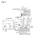
- Fig. 2 is a block diagram showing the details of the sampling circuit 140 and the data line driving circuit 150 according to the first embodiment.
- Fig. 3 is a timing chart showing the time-lapse change of various signals relating to the sampling circuit 140 and the data line driving circuit 150.
- the data line driving circuit 150 includes a bidirectional shift register 160 for sequentially driving the data lines 114 bidirectionally.
- the shift direction is determined by a direction control signal D. If the direction control signal D is high, the transfer start pulse DX is input to the bidirectional shift register 160 from the left.
- the transfer start pulse DX is sequentially shifted from left to right and is output as transfer signals SR1 to SRn from the corresponding stages SRS(i), where i represents 1, 2, 3, ..., n, of the bidirectional shift register 160.
- an inverse direction control signal D INV is positive, the transfer start pulse DX is input to the bidirectional shift register 160 from the right and is sequentially shifted from right to left.
- Enable circuits 170a and 170b constituting an example of the buffer circuit according to the present invention are arranged between the bidirectional shift register 160 and the sampling circuit 140.
- the enable circuit 170a includes a NAND circuit 171a and an inverter 172a.
- the enable circuit 170b includes a NAND circuit 171b and an inverter 172b.
- the transfer signals SR1 to SRn output from the bidirectional shift register 160 are supplied to one input of the enable circuits 170a, 170b, and so on, respectively.
- Enable signals ENB1 and ENB2 are input to the other input of the enable circuits 170a and 170b, respectively.
- the data lines 114 are driven only when the corresponding transfer signals SR1 to SRn are output and the corresponding enable signals ENB1 and ENB2 are output.
- the enable signals ENB1 and ENB2 control the corresponding data lines 114 to an active state when the image signal VID is output stably.
- sampling signals are supplied as data line driving signals or sampling circuit driving signals (hereinafter, referred to as sampling signals) S1 to Sn, which are an example of sampling pulses according to the present invention, to the sampling circuit 140.
- the sampling circuit 140 includes a plurality of sampling switches 141 each including a first-conductivity-type TFT used for sampling.
- Six data lines 114 constitute each group. For the data lines 114 belonging to each group, the six-phase serial-to-parallel converted image signals VID1 to VID6 are sampled in accordance with the sampling signals S1 to Sn and are sequentially output to the corresponding data lines 114.
- each of the data lines 114 is provided with the sampling switch 141.
- a source electrode of each of the sampling switches 141 is connected to a signal line to which one of the image signals VID1 to VID6 is supplied and a drain electrode of each of the sampling switches 141 is connected to one of the data lines 114.
- a gate electrode of each of the sampling switches 141 is connected to a signal line to which the corresponding one of the sampling signals S1 to Sn is supplied in accordance with the group.
- the image signals VID1 to VID6 are supplied at the same time, they are sampled by the sampling signal S1 at the same time.
- the image signals VID1 to VID6 are sequentially sampled by the sampling signals S1, S2, ..., Sn.
- the transfer start pulse DX input to the bidirectional shift register 160 is shifted for every half cycle of the transfer clock CLX, and data line transfer signals (hereinafter, referred to as transfer signals) SR1 to SRn, which are delayed by a half cycle of the transfer clock CLX, are sequentially output from the corresponding output stages of the bidirectional shift register 160.
- transfer signals data line transfer signals
- the transfer signals SR1 to SRn are logically multiplied by the enable signals ENB in the enable circuits 170a, 170b, and so on and are output as the sampling signals S1 to Sn. Accordingly, the image signals are in synchronization with the sampling signals (for example, the image signals VID1 to VID6 are in synchronization with the sampling signal S1). Thus, accurate display can be achieved.
- each of the transfer signals SR1 to SRn output from the corresponding stages SRS(i), where i represents 1, 2, 3, .., n, of the bidirectional shift register 160 may be divided into a plurality of signals to be output in parallel, and a plurality of sampling signals obtained by logically multiplying with the plurality of enable signals, the number of enable signals being equal to the number of divided transfer signals, may be output.
- each of the stages SRS(i) of the bidirectional shift register 160 controls a plurality of sampling circuits, so that the number of stages of the bidirectional shift register 160 can be reduced.
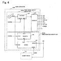
- timing generator 200 The structure and operation of the timing generator 200 according to the first embodiment will now be described in detail with reference to Fig. 4, in addition to Fig.
- the timing generator 200 includes a timing signal output circuit part 200a and a timing adjusting circuit part 200b.
- the timing signal output circuit part 200a includes an oscillator circuit 21, a counter 22, and a decoder 23.
- the oscillator circuit 21 outputs a clock signal OSCI having a frequency several times as large as a dot clock DC.
- the counter 22 is reset in synchronization with the rising edge of a horizontal synchronization signal HSYNC. After reset, the counter 22 counts the number of pulses of the clock signal OSCI.
- the counter 22 has an initial value input terminal INIT for inputting an initial value of the count rate when the counter 22 is reset.
- the decoder 23 decodes the output value of the counter 22 and outputs various timing signals, such as the dot clock DC, the transfer start pulses DX and DY, the clock signals CLX and CLY, and the inversion clock signals CLX INV and CLY INV .
- the timing adjusting circuit part 200b includes a register 25 and a counter 26.
- the counter 26 starts counting the clock signal OSCI.
- the register 25 is storing means and latches the count result of the counter 26 in synchronization with a vertical synchronization signal VSYNC.
- output pulses from the dummy circuit 27 to be described in detail later are input to the counter 26.
- the count result of the output pulses indicates a delay time of sampling signals in the buffer circuit and the sampling circuit. Since the initial value in the counter 22 is preset on the basis of the count result, timing signals, such as the dot clock DC, the transfer start pulse DX, and the clock signal CLX, are output earlier by a time corresponding to the count result.
- the timing adjusting circuit part 200b is capable of measuring a delay time by counting output pulses from the dummy circuit 27 and of performing timing adjustment of clock signals on the basis of the measured delay time.
- the dummy circuit 27 creates a detection signal MON, which is an example of a delay signal indicating the amount of delay of a sampling pulse according to the present invention.
- the detection signal MON is fed back to the bidirectional shift register 160 via the timing generator 200 so that the amount of delay of the sampling signals S1 to Sn, which are an example of the sampling pulses according to the present invention, is reduced.
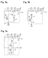
- Fig. 5 includes Fig. 5(a) showing the structure of a dummy circuit 27a according to a working example, which is the structure of the dummy circuit 27 according to the first embodiment shown in Fig. 2; Fig. 5(b) showing the structure of a dummy circuit 27b according to comparative example 1; and Fig.
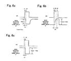
- Fig. 6 includes timing charts showing the detection state of signal delay in the dummy circuit 27a according to the working example, in the dummy circuit 27b according to comparative example 1, and in the dummy circuit 27c according to comparative example 2.
- the dummy circuit 27 since the dummy circuit 27 according to the first embodiment simulates the structure of the data line driving circuit 150 and the sampling circuit 140, the dummy circuit 27 includes a clocked inverter 271 and a clocked inverter 272.
- the clocked inverter 271 corresponds to a corresponding clocked inverter 161a, 161b, or the like constituting the bidirectional shift register 160 and the clocked inverter 272 corresponds to a corresponding clocked inverter 162a, 162b, or the like constituting the bidirectional shift register 160.
- the dummy circuit 27 further includes a NAND circuit 273 and an inverter 274.
- the NAND circuit 273 corresponds to a corresponding NAND circuit 171a, 171b, or the like constituting the buffer circuit (or the enable circuit) and the inverter 274 corresponds to a corresponding inverter 172a, 172b, or the like constituting the buffer circuit (or the enable circuit).
- the dummy circuit 27 includes a first-conductivity-type TFT 28 corresponding to the sampling switch 141 constituting the sampling circuit 140.
- the transfer start pulse DX (hereinafter, referred to as an "input signal DX" in the explanation for the dummy circuit 27), which is input to the data line driving circuit 150, is also input to the clocked inverter 271 in the dummy circuit 27.
- the source of the first-conductivity-type TFT 28 is connected to a low-potential power supply V SS in the driving circuit 120 and the drain of the first-conductivity-type TFT 28 is biased at a high-potential power supply V DD in the driving circuit 120 and is connected to a detection terminal 29.
- the detection terminal 29 is connected to the counter 26 in the timing generator 200 and the detection signal MON delayed in the dummy circuit 27a is output to the counter 26.
- the detection terminal 29 is connected to the internal power supply V DD of the liquid crystal panel 100 via a load resistor 30 and is biased at a high potential.
- dummy circuit 27 which simulates the sampling circuit 140, six first-conductivity-type TFTs 28 are connected in parallel in a similar manner.
- the dummy circuit 27 is illustrated such that one first-conductivity-type TFT 28 is connected, and the other five first-conductivity-type TFTs 28 are not shown in Figs. 2 and 5. This also applies to comparative examples 1 and 2 in Fig. 5.
- the dummy circuit 27 simulates a path corresponding to one stage of the bidirectional shift register 160, from the bidirectional shift register 160 to the sampling circuit 140.
- the sampling operation of an image signal is performed in the sampling circuit 140 by a sampling pulse generated in the data line driving circuit 150, and at the same time, a delay signal indicating the amount of delay of the sampling pulse is generated in the dummy circuit 27 to be detected as a detection signal MON in the detection terminal 29.
- the timing adjusting circuit part 200b of the timing generator 200 measures the delay time, as described above, on the basis of the detection signal MON.
- the detection signal MON which is a delay signal
- in the dummy circuit 27 is fed back to the bidirectional shift register 160 so that the amount of delay of the sampling pulse is reduced.
- the accuracy of delay time measurement is determined in accordance with how well the characteristics of the dummy circuit 27, which is a detection circuit of a delay signal, simulates the characteristics of the sampling circuit 140 and the data line driving circuit 150. Accordingly, with the structure described above, the dummy circuit 27 can detect a delay time of a sampling pulse with a relatively high accuracy, thus reducing the adverse influence of the delay of the sampling pulse upon a display image.
- the dummy circuit 27 be formed on the device substrate of the liquid crystal panel 100 in the same process as elements of the data line driving circuit 150 and the sampling circuit 140, which are to be simulated. It is also preferable that the size of elements in the dummy circuit 27 be equal to the size of the corresponding elements in the sampling circuit 140 and the data line driving circuit 150. Also, it is preferable that the channel width of the first-conductivity-type TFTs 28 be equal to the channel width of the corresponding sampling switches 141.
- the degree of how well the dummy circuit 27 simulates the data line driving circuit 150 and the sampling circuit 140 is further increased, thus achieving a very high accuracy in detecting the amount of delay of a sampling pulse.
- each of the first-conductivity-type TFTs 28 include an N-channel TFT.
- each of the first-conductivity-type TFTs 28 includes a P-channel TFT (in this case, a carrier is a positive hole)
- higher carrier mobility and a higher switching reaction rate to an input signal "ON” (an input signal "OFF" for a P-channel) for the gate can be achieved.
- a delay signal can be detected with a relatively high accuracy.
- each of the sampling switches 141 in the sampling circuit 140 includes a P-channel TFT
- the dummy circuit 27 may also include P-channel TFTs. Even if the P-channel TFTs are used, the sampling switches 141 can be accurately simulated. Thus, the amount of delay of a sampling pulse is detected with high accuracy. Consequently, a similar advantage can be achieved in terms of reduction in the adverse influence of a delay.
- dummy circuit 27 The operation of the dummy circuit 27 according to the first embodiment will now be described with reference to Figs. 5 and 6. In particular, advantages of the dummy circuit 27 according to the first embodiment will be explained by comparing it with the dummy circuit 27b according to comparative example 1 and the dummy circuit 27c according to comparative example 2.
- the first-conductivity-type TFT 28 of the dummy circuit 27b according to comparative example 1 is connected in a different manner than the first-conductivity-type TFT 28 of the dummy circuit 27a according to the working example shown in Fig. 5(a).
- An input signal DX is delayed by the elements from the clocked inverter 271 to the inverter 274 and is input to the gate in a similar manner.
- the source is connected to the internal power supply V DD of the liquid crystal panel 100 via the load resistor 30 to be biased at a high potential.
- the drain is connected to the detection terminal 29, and the output signal can be extracted as a detection signal MON indicating a delay time from the detection terminal 29.
- a complementary TFT such as an inverter 31 made of a complementary MOS (CMOS) TFT, is connected in the dummy circuit 27c according to comparative example 2, and the output signal can be extracted as a detection signal MON indicating a delay time from the detection terminal 29.
- CMOS complementary MOS
- an input signal DX is inverted four times via the clocked inverter 271, the clocked inerter 272, the NAND circuit 273, and the inverter 274 while being delayed and is supplied to the gate of the first-conductivity-type TFT 28.
- the drain of the first-conductivity-type TFT 28 is biased at a voltage obtained by reducing the potential of the internal power supply V DD by the load resistor 30.
- the first-conductivity-type TFT 28 including an N-channel TFT becomes an "ON" state, and current flows to the low-potential power supply V SS connected to the source of the first-conductivity-type TFT 28.
- a signal at the detection terminal 29 connected to the drain becomes an "L" level and the signal is detected as a falling signal due to the "ON" state of the first-conductivity-type TFT 28.
- a time difference of ⁇ t minutes is generated between time t1 at which the input signal DX rises to the "H” level and time t2 at which the detection signal MON falls due to signal delay when the signal passes through the elements 271 to 274 and the operation of the first-conductivity-type TFT.
- the input signal DX and the falling edge detection signal MON are compared with each other and counted by the counter 26 of the timing generator 200 to measure the time difference ⁇ t as a delay time of the sampling pulse.
- the dummy circuit 27a detects the falling edge from a state in which the voltage of the detection terminal 29 is already biased.
- the operation time of the switching itself of the delay time ⁇ t can be reduced to a negligible amount. Consequently, the amount of delay of the sampling pulse can be detected with very high accuracy, and adjustment corresponding to such a high accuracy can also be achieved.
- the voltage of the high-potential power supply V DD is reduced via the load resistor 30 and the drain of the first-conductivity-type TFT 28 is biased at a relatively low potential.
- the power supply voltage V DD is reduced in advance so that the drain of the first-conductivity-type TFT 28 is biased at a relatively low potential.
- the first-conductivity-type TFT 28 does not need high breakdown voltage characteristics.
- the inverter 31 has a structure different from the sampling switch 141.
- the inverter 31 is different from the sampling switch 141 in that the inverter 31 includes a complementary TFT composed of at least an N-channel TFT and at least a P-channel TFT.
- the size (in particular, the channel width) of the inverter 31 is different from that of the sampling switch 141.
- the first-conductivity-type TFT 28 has the same structure as the sampling switch 141, and it is obvious that, as compared with comparative example 2, the working example is advantageous in measuring a delay time with high accuracy.
- the bias of the internal power supply V DD of a relatively high potential is directly applied as described above.
- This causes disadvantages in terms of the breakdown voltage characteristics required for each TFT element, as compared with the dummy circuit 27a according to the working example.
- the load resistor 30 is used and bias is applied after reducing the voltage, as in the dummy circuit 27a according to the working example or the dummy circuit 27b according to comparative example 1, signal rounding that is not negligible occurs when the detection signal MON rises, as in the dummy circuit 27b according to comparative example 1.
- this structure causes disadvantages in terms of accuracy in measuring signal delay, as compared with the dummy circuit 27a according to the working example.
- Comparative examples 1 and 2 shown in Figs. 5(b) and 5(c), respectively, are comparative examples for explaining outstanding advantages of the working example of the first embodiment shown in Fig. 5(a) and are not excluded from the electro-optical device according to the present invention.
- comparative examples 1 and 2 shown in Figs. 5(b) and 5(c) are included in the technical scope of the present invention.
- comparative examples 1 and 2 have drawbacks as compared with the working example shown in Fig. 5(a), corresponding advantages can be achieved as compared with the conventional examples described above.
- the electro-optical device according to the second embodiment is different from the electro-optical device according to the first embodiment in the size or the planar pattern of component parts of the dummy circuit 27.
- the circuit structure and operation of the dummy circuit 27, the structure of the liquid crystal device, and the structure and operation of the circuits in the liquid crystal panel 100 according to the second embodiment are similar to those according to the first embodiment. Thus, only parts that are different from the first embodiment will be explained below. Since all component parts according to the first embodiment correspond to those according to the second embodiment, they are not illustrated here.
- the dummy circuit 27 also includes the plurality of first-conductivity-type TFTs 28, which simulate the sampling switches 141, connected in parallel and the number of first-conductivity-type TFTs 28 is equal to the number of sampling switches 141.
- the same delay time can be detected.
- This structure requires a relatively large space on the limited device substrate of the liquid crystal panel 100 in terms of layout design.
- the dummy circuit 27 according to the second embodiment is arranged in a space as small as possible on the assumption that the dummy circuit 27 is provided on the same device substrate, as in the first embodiment.
- a method for arranging the dummy circuit 27 as described above will now be described.
- the channel width of the first-conductivity-type TFT 28 in the dummy circuit 27 is smaller than the channel width of the sampling switch 141 of the sampling circuit 140.
- the ratio of the size of the sampling switch 141 of the sampling circuit 140 to the size of the buffer circuit (that is, the enable circuit 170a, 170b, or the like) in the preceding stage is equal to the ratio of the size of the first-conductivity-type TFT 28 of the corresponding dummy circuit 27 to the size of the buffer circuit (that is, the NAND circuit 273 and the inverter 274) located in the preceding stage.
- the ratio of the size of the first-conductivity-type TFT 28 of the dummy circuit 27 to the size of all other component parts may be equal to the ratio of the size of the sampling switch 141, which is to be simulated, to the size of component parts (for example, inverters 161a, 162a, 171a, 172a) for one stage of a shift register up to the sampling circuit 140.
- the size of all other component parts may be reduced by the same ratio.
- the ratio of the capacitance of the first-conductivity-type TFT 28 to the capacitance of all component parts in the preceding stage is equal to the ratio of the capacitance of the sampling switch 141 in the circuit to be simulated to the capacitance of all component parts in the preceding stage.
- the electro-optical device according to the third embodiment is different from the electro-optical device according to the first embodiment in the structure of the dummy circuit 27 and the enable circuits 170a, 170b, and the like constituting an example of the buffer circuit in the data line driving circuit 150.
- the operation of the dummy circuit 27 and the structure and operation of the liquid crystal device according to the third embodiment are similar to those according to the first embodiment. Thus, only parts that are different from the first embodiment will be explained below.
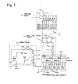
- each of the enable circuits 170a, 170b, and so on which is an example of the buffer circuit, includes inverters provided in a plurality of stages.
- inverters 173a and 174a are added to the structure according to the first embodiment.
- the dummy circuit 27 that simulates the enable circuit described above to detect signal delay also includes inverters provided in a plurality of stages, the number of stages in the dummy circuit 27 being equal to the number of stages in the enable circuit, as shown in Fig. 7.
- inverters 275 and 276 are added as compared with the dummy circuit 27 according to the first embodiment.
- the dummy circuit 27 is formed on the device substrate of the liquid crystal panel 100 in the same process as elements of the sampling circuit 140 and the data line driving circuit 150. Also, the size of elements of the dummy circuit 27 is equal to the size of the corresponding elements of the sampling circuit 140 and the data line driving circuit 150 to be simulated. Also, in the third embodiment, in particular, the channel width of the first-conductivity-type TFTs 28 is equal to the channel width of the corresponding sampling switches 141.
- the degree of simulation of the data line driving circuit 150 and the sampling circuit 140 by the dummy circuit 27 is further increased.
- the amount of delay of a sampling pulse can be detected with very high accuracy.
- the other structure and operation of the dummy circuit 27 are the same as those according to the first embodiment.
- the amount of delay of the sampling pulse can be detected with high accuracy similar to the first embodiment.
- the electro-optical device according to the fourth embodiment is different from the electro-optical device according to the third embodiment in the size or the planar pattern of the component parts of the dummy circuit 27.
- the circuit structure and operation of the dummy circuit 27, the structure of the liquid crystal device, and the structure and operation of the circuits in the liquid crystal panel 100 are similar to those according to the third embodiment. Thus, only parts that are different from the third embodiment will be explained. Since all component parts according to the third embodiment correspond to those according to the fourth embodiment, they are not illustrated here.
- the channel width of the first-conductivity-type TFT 28 of the dummy circuit 27 is smaller than the channel width of the sampling switch 141 of the sampling circuit 140.
- forming a compact dummy circuit on a limited space on the substrate avoids the problem of space shortage.
- miniaturization of the substrate and the entire electro-optical panel, including an area required for forming a dummy circuit may be achieved.
- the ratio of the size of the first-conductivity-type TFT 28 of the dummy circuit 27 to the size of the inverter 276 in the final stage of the buffer circuit in the preceding stage is equal to the ratio of the size of the sampling switch 141 of the sampling circuit 140 to the size of the inverter 174a in the final stage of the buffer circuit in the preceding stage.
- the ratio of the size of the first-conductivity-type TFT 28 of the dummy circuit 27 to the size of all other component parts may be equal to the ratio of the size of the sampling switch 141, which is to be simulated, to the size of component parts (for example, inverters 161a, 162a, 171a, 172a, 173a, and 174a) of one stage of the shift register up to the sampling circuit 140.
- component parts for example, inverters 161a, 162a, 171a, 172a, 173a, and 174a
- the ratio of the capacitance of the first-conductivity-type TFT 28 to the capacitance of all component parts in the preceding stage is equal to the ratio of the capacitance of the sampling switch 141 of the circuit to be simulated to the capacitance of all component parts in the preceding stage.
- the bidirectional shift register 160 may be formed on the substrate constituting the liquid crystal panel 100 as an IC attached externally or attached later.
- the bidirectional shift register 160 can be mounted relatively easily.
- the dummy circuit is formed on the same substrate as the buffer circuit and the sampling circuit, which are simulated by the dummy circuit, the degree of simulation by the dummy circuit 27 can be increased.
- the dummy circuit 27 is formed in the same process as elements of the data line driving circuit 150 and the sampling circuit 140 in the liquid crystal panel 100, and the dummy circuit 27 functions as a simulation circuit having the same circuit structure. A falling edge of a signal is detected with a quick switching operation. Thus, a delay signal that is equal to the actual signal delay of a sampling pulse can detected, the delay time can be measured with high accuracy, and the detection signal can be fed back to the driving circuit.
- the dummy circuit according to the first to fourth embodiments simulates the clocked inverters and the enable circuit in the data line driving circuit and the sampling circuit relatively accurately.
- a dummy circuit may simulate at least part of the data line driving circuit, the buffer circuit (enable circuit), and the sampling circuit. Even in this case, the delay time can be measured with an accuracy corresponding to the degree of simulation, and the adverse influence of the delay can be correspondingly reduced by feeding back a delay signal.
- simulating one or more circuit parts that mainly cause delay or that constrain the delay among the data line driving circuit, the enable circuit, and the sampling circuit effectively prevents the adverse influence of the delay.
- simulating an inverter in the final stage in the buffer circuit from among the inverters in the plurality of stages connected in series effectively reduces the adverse influence of the delay.
- a partial simulation by the dummy circuit reduces the area in the limited space on the device substrate on which the dummy circuit is formed.
- this structure is advantageous in reducing the size of the device substrate and the entire device.
- Fig. 8 is a plan view of the liquid crystal device substrate 10, which is a TFT array substrate, and each component part provided on the liquid crystal device substrate 10 when viewed from the side of an opposing substrate 20.
- Fig. 9 is a cross-sectional view taken along the line H-H' of Fig. 8.
- a seal member 52 is provided around the image display area 110 (that is, an area of the liquid crystal device in which an image is displayed in accordance with a change in the orientation state of a liquid crystal layer 50) defined by the plurality of pixel electrodes 118 on the liquid crystal device substrate 10.
- the seal member 52 is made of a photocurable resin and bonds the substrates around the image display area 110 to surround the liquid crystal layer 50.
- a frame-shaped light-shielding film 53 is provided on the opposing substrate 20 between the image display area 110 and the seal member 52.
- the frame-shaped light-shielding film 53 and a light-shielding layer 23 may be provided on the liquid crystal device substrate 10.
- the scanning line driving circuits 130 are provided in parts along the left and right sides of the image display area 110. If driving delay of the scanning lines 112 does not cause a big problem, the scanning line driving circuit 130 may be provided only on one side of the scanning lines 112.
- the data line driving circuit 150 and an external circuit connection terminal 102 for inputting a signal from the outside are provided along the lower side of the image display area 110 in an area outside the seal member 52.
- the scanning line driving circuits 130 are provided along the left and right sides of the image display area 110.
- the data line driving circuits 150 may be provided along the upper and lower sides of the image display area 110. In this case, for example, data lines in odd-numbered columns may be electrically connected to one of the data line driving circuits 150 and data lines in even-numbered columns may be electrically connected to the other one of the data line driving circuits 150, so that data lines are driven from the upper and lower sides like combs.
- a plurality of wiring lines 105 for supplying a power supply and a driving signal to the scanning line driving circuits 130 is provided in the upper side of the image display area 110.
- an upper and lower conductive material 106 for electrically connecting the liquid crystal device substrate 10 and the opposing substrate 20 is provided at at least one corner of the opposing substrate 20.
- the opposing substrate 20 having an outline substantially equal to the seal member 52 is fixed to the liquid crystal device substrate 10 using the seal member 52.
- control circuit for outputting a clock signal, an image signal, and the like to the data line driving circuit 150 and the scanning line driving circuit 130 is provided outside the liquid crystal device in the embodiments described above, the present invention is not limited to this.
- the control circuit may be provided in the liquid crystal device.
- a clock signal may be supplied from the external control circuit and a circuit for generating a counter-phase clock signal may be provided on the liquid crystal device substrate.
- the liquid crystal device described above may be a color liquid crystal projector or the like.
- three liquid crystal devices are used as light valves for R, G, and B, respectively.
- Light of each color separated by a dichroic mirror for RGB color separation enters each panel as incident light.
- a color filter is not provided on the opposing substrate 20.
- RGB color filters may be provided, together with a protective film for the color filters, in predetermined areas of the opposing substrate 20 that are not provided with the light-shielding layer 23 and that face the pixel electrodes 118.
- the liquid crystal device according to the present invention may also be a color liquid crystal device, such as a color liquid crystal television of a direct viewing type or a reflection type, other than a liquid crystal projector.
- the switching element used for the liquid crystal device may be a positive staggered or coplanar polysilicon TFT.
- the switching element used in the present invention is applicable to a TFT of other types, such as an inverted-staggered TFT and an amorphous silicon TFT.
- the liquid crystal layer 50 is made of nematic liquid crystal, as an example, in the liquid crystal device.
- use of macromolecule distributed liquid crystal in which liquid crystal is distributed as microparticles in a macromolecule eliminates the necessity of an alignment film, the polarization film, a polarization plate, and the like.
- an increase in the brightness of the liquid crystal device and a reduction in the power consumption due to an increased light utilization efficiency can be achieved.
- the data line driving circuit 150 and the scanning line driving circuit 130 may be electrically and mechanically connected to a driving LSI mounted on a tape automated bonding (TAB) substrate via an anisotropic conductive film provided near the liquid crystal device substrate 10.
- TAB tape automated bonding
- a shift register part can be arranged in a similar manner to the data line driving circuit 150.
- the electro-optical device may be an electrophoretic device, an electroluminescent (EL) device, a device using an electron emission element (a field emission display and a surface conduction electron-emitter display), or the like.
- EL electroluminescent
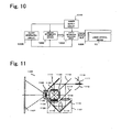
- Fig. 10 schematically shows the structure of the electronic apparatus provided with the liquid crystal device 1.
- the electronic apparatus includes a display information output source 1000, the external display information processing circuit 1002 described above, a display driving circuit 1004 including the scanning line driving circuit 130 and the data line driving circuit 150, the liquid crystal device 1, a clock generating circuit 1008, and a power supply circuit 1010.
- the display information output source 1000 includes memories, such as a read only memory (ROM), a random access memory (RAM), and an optical disk device, and a tuning circuit for outputting a tuned television signal.
- the display information output source 1000 outputs display information, such as an image signal in a predetermined format, to the display information processing circuit 1002 on the basis of a clock signal from the clock generating circuit 1008.
- the display information processing circuit 1002 includes various known processing circuits, such as an amplifying and polarity-reversing circuit, a phase expansion circuit, a rotation circuit, a gamma correction circuit, and a clamping circuit.
- the display information processing circuit 1002 sequentially generates a digital signal from the display information input on the basis of the clock signal from the clock generating circuit 1008 and outputs the digital signal, together with the clock signal CLK, to the display driving circuit 1004.
- the display driving circuit 1004 drives the liquid crystal device 1 using the driving method described above by the scanning line driving circuit 130 and the data line driving circuit 150.
- the power supply circuit 1010 supplies predetermined power to each of the circuits described above.
- the display driving circuit 1004 may be mounted on the liquid crystal device substrate constituting the liquid crystal device 1, and the display information processing circuit 1002 may also be mounted on the liquid crystal device substrate.
- the electronic apparatus having such a structure may be a liquid crystal projector shown in Fig. 11, a multimedia-compatible personal computer (PC) and an engineering workstation (EWS) shown in Fig. 12, a mobile telephone, a word processor, a television set, a viewfinder type or monitor direct-view type video tape recorder, an electronic notebook, an electronic desk calculator, a car navigation system, a POS terminal, a device provided with a touch panel, or the like.
- PC personal computer
- EWS engineering workstation
- a liquid crystal projector 1100 which is an example of the electronic apparatus, is of a projection type and includes a light source 1110, dichroic mirrors 1113 and 1114, reflecting mirrors 1115, 1116, and 1117, an incident lens 1118, a relay lens 1119, an exit lens 1120, liquid crystal light valves 1122, 1123, and 1124, a cross-dichroic prism 1125, and a projector lens 1126.
- the liquid crystal light valves 1122, 1123, and 1124 are three liquid crystal display modules each including the liquid crystal device 1 including the display driving circuit 1004 mounted on the liquid crystal device substrate and are used as liquid crystal light valves.
- the light source 1110 includes a lamp 1111, such as a metal halide lamp, and a reflector 1112 reflecting the light from the lamp 1111.
- the blue and green light reflecting dichroic mirror 1113 transmits red light from among the white light from the light source 1110 and reflects blue and green light.
- the transmitted red light is reflected by the reflecting mirror 1117 and is input to the liquid crystal light valve 1122 for red light.
- Green light from among color light reflected by the dichroic mirror 1113 is reflected by the green light reflecting dichroic mirror 1114 and is input to the liquid crystal light valve 1123 for green light.
- the second dichroic mirror 1114 transmits blue light.
- light guiding means 1121 including a relay lens system including the incident lens 1118, the relay lens 1119, and the exit lens 1120 is provided for blue light.
- the blue light is input to the liquid crystal light valve 1124 for blue light via the light guiding means 1121.
- Light of three colors modulated by the corresponding light valves is input to the cross-dichroic prism 1125.
- the prism includes four right-angle prisms attached together and a dielectric multilayer film reflecting red light and a dielectric multilayer film reflecting blue light are arranged so as to cross each other on the internal surfaces.
- the light of three colors is combined by the dielectric multilayer films to form light indicating a color image.
- the combined light is projected on a screen 1127 by the projector lens 1126, which is a projection optical system, and the image is magnified to be displayed.
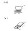
- a laptop personal computer 1200 which is another example of the electronic apparatus, includes a liquid crystal display 1206 including the liquid crystal device 1 accommodated in a top cover case thereof and a main unit 1204 containing a CPU, a memory, a modem, and the like and including a keypad 1202 mounted thereon.
- one of two transparent substrates 1304a and 1304b constituting a liquid crystal device substrate 1304 is connected to a tape carrier package (TCP) 1320 including an IC chip 1324 mounted on polyimide tape 1322 provided with a metal transparent conductive film.
- TCP tape carrier package
- Such a device arranged as described above can be manufactured, sold, and used as a liquid crystal device functioning as a component of the electronic apparatus.
- a liquid crystal television set As described above, in addition to the electronic apparatuses described above with reference to Figs. 11 to 13, a liquid crystal television set, a view-finder type or monitor direct-view type video tape recorder, a car navigation system, an electronic notebook, a calculator, a word processor, a workstation, a mobile telephone, a television telephone, a POS terminal, a device provided with a touch panel, and the like are examples of the electronic apparatus shown in Fig. 10.
Landscapes
- Engineering & Computer Science (AREA)
- Chemical & Material Sciences (AREA)
- Crystallography & Structural Chemistry (AREA)
- Physics & Mathematics (AREA)
- Computer Hardware Design (AREA)
- General Physics & Mathematics (AREA)
- Theoretical Computer Science (AREA)
- Liquid Crystal Display Device Control (AREA)
- Control Of Indicators Other Than Cathode Ray Tubes (AREA)
- Liquid Crystal (AREA)
- Photovoltaic Devices (AREA)
Abstract
Description
Claims (14)
- An electro-optical panel driving circuit for driving an electro-optical panel including pixel electrodes; switching elements for switching on and off the corresponding pixel electrodes; and data lines for supplying image signals to the corresponding pixel electrodes via the corresponding switching elements, the pixel electrodes, the switching elements, and the data lines being provided on a substrate, the electro-optical panel driving circuit comprising:wherein delay signals indicating the amount of delay of the sampling pulses and generated by the dummy circuit (27) are fed back to the shift register circuit (160) so that the amount of delay is reduced, anda shift register circuit (160) that sequentially outputs transfer signals;a buffer circuit (170a, 170b) that buffers the sequentially output transfer signals;a sampling circuit (140) that samples the image signals using the buffered transfer signals as sampling pulses and that supplies the sampled image signals to the corresponding data lines; anda dummy circuit (27) that simulates at least part of the buffer circuit (170a, 170b) and the sampling circuit (140),
wherein the buffer circuit (170a, 170b), the sampling circuit (140), and the dummy circuit (27) are provided on the substrate. - An electro-optical panel driving circuit according to Claim 1, wherein the shift register circuit (160) is provided in an integrated circuit externally attached to the substrate.
- An electro-optical panel driving circuit according to Claim 1 or 2, wherein the buffer circuit (170a, 170b) includes a plurality of stages of buffers connected in series,
wherein the sampling circuit (140) includes analog sampling switches, and
wherein the dummy circuit (27) simulates at least the buffer in the final stage among the plurality of stages of buffers. - An electro-optical panel driving circuit according to Claim 3, wherein the dummy circuit (27) simulates the sampling switches and all of the plurality of stages of buffers.
- An electro-optical panel driving circuit according to any one of Claims 1 to 4,
wherein semiconductor elements constituting the sampling circuit (140) are formed in the same process and at the same time as semiconductor elements constituting the corresponding dummy circuit (27). - An electro-optical panel driving circuit according to Claim 5, wherein each of the semiconductor elements is an N-type semiconductor element.
- An electro-optical panel driving circuit according to Claim 5 or 6, further comprising a timing adjusting circuit,
wherein each of the semiconductor elements is a thin-film transistor,
wherein the source of the thin-film transistor is connected to a low-potential power supply of the driving circuit and the drain of the thin-film transistor is biased at a high-potential power supply of the driving circuit and is connected to a detection terminal of the driving circuit,
wherein the shift register circuit (160) sequentially outputs the transfer signals in accordance with a clock cycle of clock signals, and
wherein the timing adjusting circuit adjusts the timing of the clock signals input to the shift register circuit (160) on the basis of the timing of the falling edge of the delay signals detected by the detection terminal. - An electro-optical panel driving circuit according to any one of Claims 1 to 6, further comprising a timing adjusting circuit,
wherein the shift register circuit (160) sequentially outputs the transfer signals in accordance with a clock cycle of clock signals, and
wherein the timing adjusting circuit adjusts the timing of the clock signals input to the shift register circuit (160) on the basis of the amount of delay indicated by the delay signals. - An electro-optical panel driving circuit according to Claim 8, wherein the shift register circuit (160) and the timing adjusting circuit are provided in an integrated circuit externally attached to the substrate.
- An electro-optical panel driving circuit according to any one of Claims 1 to 9, wherein the channel width of first thin-film transistors constituting the sampling circuit (140) is equal to the channel width of second thin-film transistors constituting the dummy circuit (27), the second thin-film transistors corresponding to the first thin-film transistors.
- An electro-optical panel driving circuit according to any one of Claims 1 to 10, wherein the channel width of second thin-film transistors constituting the dummy circuit (27), the second thin-film transistors corresponding to first thin-film transistors constituting the sampling circuit (140), is smaller than or equal to the channel width of the first thin-film transistors, and
wherein the ratio of the size of the first thin-film transistors to the size of a first buffer circuit (170a, 170b) in the preceding stage of the first thin-film transistors is equal to the ratio of the size of the second thin-film transistors of the dummy circuit (27) to the size of a second buffer circuit in the preceding stage of the second thin-film transistors. - An electro-optical panel driving circuit according to any one of Claims 1 to 10, wherein the buffer circuit (170a, 170b) includes a plurality of stages of buffers connected in series,
wherein the sampling circuit (140) includes analog sampling switches,
wherein the channel width of second thin-film transistors constituting the dummy circuit (27), the second thin-film transistors corresponding to first thin-film transistors functioning as the sampling switches, is smaller than or equal to the channel width of the first thin-film transistors, and
wherein the ratio of the size of the first thin-film transistors to the size of the buffer in the final stage of the first buffer circuit (170a, 170b) in the preceding stage of the first thin-film transistors is equal to the ratio of the size of the second thin-film transistors of the dummy circuit (27) to the size of the buffer in the final stage of a second buffer circuit in the preceding stage of the second thin-film transistors. - An electro-optical device comprising the electro-optical panel driving circuit as set forth in any one of Claims 1 to 12 and the electro-optical panel driven by the driving circuit.
- An electronic apparatus comprising the electro-optical device as set forth in Claim 13.
Applications Claiming Priority (4)
| Application Number | Priority Date | Filing Date | Title |
|---|---|---|---|
| JP2003133278 | 2003-05-12 | ||
| JP2003133278 | 2003-05-12 | ||
| JP2004044661 | 2004-02-20 | ||
| JP2004044661A JP2004361919A (en) | 2003-05-12 | 2004-02-20 | Driving circuit for electro-optical panel, and electro-optical device and electronic apparatus having the same |
Publications (2)
| Publication Number | Publication Date |
|---|---|
| EP1477962A2 true EP1477962A2 (en) | 2004-11-17 |
| EP1477962A3 EP1477962A3 (en) | 2006-10-25 |
Family
ID=33032383
Family Applications (1)
| Application Number | Title | Priority Date | Filing Date |
|---|---|---|---|
| EP04252593A Withdrawn EP1477962A3 (en) | 2003-05-12 | 2004-05-05 | Electro-optical panel driving circuit, electro-optical device provided with electro-optical panel and driving circuit, and electronic apparatus provided with electro-optical device |
Country Status (6)
| Country | Link |
|---|---|
| US (1) | US20040239610A1 (en) |
| EP (1) | EP1477962A3 (en) |
| JP (1) | JP2004361919A (en) |
| KR (1) | KR100612630B1 (en) |
| CN (1) | CN100351891C (en) |
| TW (1) | TWI239504B (en) |
Cited By (3)
| Publication number | Priority date | Publication date | Assignee | Title |
|---|---|---|---|---|
| CN100397445C (en) * | 2005-10-10 | 2008-06-25 | 义隆电子股份有限公司 | Display driving device and method |
| CN102339189A (en) * | 2008-06-30 | 2012-02-01 | 株式会社日立显示器 | Touch panel |
| CN111383553A (en) * | 2018-12-28 | 2020-07-07 | 乐金显示有限公司 | display device |
Families Citing this family (19)
| Publication number | Priority date | Publication date | Assignee | Title |
|---|---|---|---|---|
| JP4534743B2 (en) * | 2004-12-14 | 2010-09-01 | セイコーエプソン株式会社 | Electro-optical device and electronic apparatus |
| JP2006251122A (en) * | 2005-03-09 | 2006-09-21 | Seiko Epson Corp | Liquid crystal panel drive device and image display device |
| US7868883B2 (en) * | 2005-05-27 | 2011-01-11 | Seiko Epson Corporation | Electro-optical device and electronic apparatus having the same |
| JP5007495B2 (en) * | 2005-07-21 | 2012-08-22 | セイコーエプソン株式会社 | Electro-optical device and electronic apparatus |
| JP4400593B2 (en) * | 2006-05-19 | 2010-01-20 | セイコーエプソン株式会社 | Electro-optical device, driving method thereof, and electronic apparatus |
| JP4884909B2 (en) * | 2006-10-03 | 2012-02-29 | 株式会社 日立ディスプレイズ | Display device |
| KR101344835B1 (en) * | 2006-12-11 | 2013-12-26 | 삼성디스플레이 주식회사 | Method for decreasing of delay gate driving signal and liquid crystal display using thereof |
| JP4998142B2 (en) * | 2007-08-23 | 2012-08-15 | セイコーエプソン株式会社 | Electro-optical device and electronic apparatus |
| JP2009075507A (en) * | 2007-09-25 | 2009-04-09 | Seiko Epson Corp | Electro-optical device inspection method and electro-optical device manufacturing method |
| JP4452306B2 (en) * | 2007-12-26 | 2010-04-21 | シャープ株式会社 | Pulse signal delay circuit and LED drive circuit |
| US7971158B2 (en) * | 2008-06-23 | 2011-06-28 | International Business Machines Corporation | Spacer fill structure, method and design structure for reducing device variation |
| JP5407311B2 (en) * | 2008-12-09 | 2014-02-05 | セイコーエプソン株式会社 | Electro-optical device and electronic apparatus |
| JP6204025B2 (en) * | 2013-03-05 | 2017-09-27 | シナプティクス・ジャパン合同会社 | Driver IC |
| KR102285392B1 (en) * | 2015-02-03 | 2021-08-04 | 삼성디스플레이 주식회사 | Sensing apparatus, Display apparatus, and Method of sensing electrical signal |
| CN108573681B (en) * | 2017-03-13 | 2020-12-15 | 群创光电股份有限公司 | Display device and driving method thereof |
| TWI643013B (en) * | 2017-03-29 | 2018-12-01 | 友達光電股份有限公司 | Display |
| KR102293145B1 (en) * | 2017-06-09 | 2021-08-26 | 삼성전자주식회사 | Display driving device including source driver and timing controller and operating method of display driving device |
| JP6531787B2 (en) | 2017-06-26 | 2019-06-19 | セイコーエプソン株式会社 | Electro-optical device and electronic apparatus |
| CN109961729B (en) * | 2019-04-30 | 2022-11-08 | 深圳市华星光电半导体显示技术有限公司 | Display panel and test method thereof |
Family Cites Families (3)
| Publication number | Priority date | Publication date | Assignee | Title |
|---|---|---|---|---|
| JP3424387B2 (en) * | 1995-04-11 | 2003-07-07 | ソニー株式会社 | Active matrix display device |
| JP3704911B2 (en) * | 1997-10-20 | 2005-10-12 | セイコーエプソン株式会社 | Drive circuit, display device, and electronic device |
| JP2001282171A (en) * | 2000-03-30 | 2001-10-12 | Sharp Corp | Image display device and drive control circuit thereof |
-
2004
- 2004-02-20 JP JP2004044661A patent/JP2004361919A/en active Pending
- 2004-04-16 US US10/825,305 patent/US20040239610A1/en not_active Abandoned
- 2004-04-28 TW TW093111893A patent/TWI239504B/en not_active IP Right Cessation
- 2004-04-29 CN CNB2004100374720A patent/CN100351891C/en not_active Expired - Lifetime
- 2004-05-05 EP EP04252593A patent/EP1477962A3/en not_active Withdrawn
- 2004-05-12 KR KR1020040033291A patent/KR100612630B1/en not_active Expired - Lifetime
Cited By (5)
| Publication number | Priority date | Publication date | Assignee | Title |
|---|---|---|---|---|
| CN100397445C (en) * | 2005-10-10 | 2008-06-25 | 义隆电子股份有限公司 | Display driving device and method |
| CN102339189A (en) * | 2008-06-30 | 2012-02-01 | 株式会社日立显示器 | Touch panel |
| CN102339188B (en) * | 2008-06-30 | 2015-08-26 | 株式会社日本显示器 | Touch-screen |
| CN111383553A (en) * | 2018-12-28 | 2020-07-07 | 乐金显示有限公司 | display device |
| CN111383553B (en) * | 2018-12-28 | 2022-02-11 | 乐金显示有限公司 | Display device |
Also Published As
| Publication number | Publication date |
|---|---|
| KR20040097927A (en) | 2004-11-18 |
| EP1477962A3 (en) | 2006-10-25 |
| TW200502913A (en) | 2005-01-16 |
| KR100612630B1 (en) | 2006-08-14 |
| CN100351891C (en) | 2007-11-28 |
| TWI239504B (en) | 2005-09-11 |
| CN1551091A (en) | 2004-12-01 |
| JP2004361919A (en) | 2004-12-24 |
| US20040239610A1 (en) | 2004-12-02 |
Similar Documents
| Publication | Publication Date | Title |
|---|---|---|
| EP1477962A2 (en) | Electro-optical panel driving circuit, electro-optical device provided with electro-optical panel and driving circuit, and electronic apparatus provided with electro-optical device | |
| US6580423B1 (en) | Driving circuit for electro-optical device, electro-optical device, and electronic apparatus | |
| US6670943B1 (en) | Driving circuit system for use in electro-optical device and electro-optical device | |
| JP2001166748A (en) | Electro-optical device, clock signal adjustment method and circuit thereof, production method thereof, and electronic apparatus | |
| US7277091B2 (en) | Driving circuit for electro-optical panel, electro-optical device having the driving circuit, and electronic apparatus having the electro-optical device | |
| JP3536653B2 (en) | Data line driving circuit of electro-optical device, electro-optical device, and electronic apparatus | |
| JP3520756B2 (en) | Driving circuit of electro-optical device, electro-optical device, and electronic apparatus | |
| TW200402027A (en) | Electro-optical device, drive device and drive method for electro-optical device, and electronic apparatus | |
| JPH11265162A (en) | Electro-optical devices and electronic equipment | |
| US20070285383A1 (en) | Electro-optical device, method for driving electro-optical device, and electronic apparatus | |
| US7518590B2 (en) | Driving circuit and driving method of electro-optical device, electro-optical device, and electronic apparatus | |
| JP3484963B2 (en) | Driving circuit for electro-optical device, electro-optical device, and electronic apparatus | |
| JP5407311B2 (en) | Electro-optical device and electronic apparatus | |
| JP3893819B2 (en) | Electro-optical device drive circuit, data line drive circuit, scanning line drive circuit, electro-optical device, and electronic apparatus | |
| JP2000047643A (en) | Driving circuit for electro-optical device and electro-optical device having the same | |
| JP5007495B2 (en) | Electro-optical device and electronic apparatus | |
| CN100466055C (en) | Drive circuit for electro-optic device, electro-optic device and electronic device having same | |
| JP2001188520A (en) | Driving circuit of electro-optical device, electro-optical device, and electronic apparatus | |
| JP4419394B2 (en) | Electro-optical panel driving method and driving circuit, electro-optical panel using the same, and electronic apparatus | |
| JP2004046201A (en) | Drive circuit, electro-optical device, and electronic equipment | |
| CN100412630C (en) | Electro-optical device, driving device, driving method and electronic device thereof | |
| JP4720654B2 (en) | Electro-optical device drive circuit, electro-optical device, and electronic apparatus | |
| JP2004109987A (en) | Electro-optical devices and electronic equipment | |
| JP2006243759A (en) | Electro-optical device drive circuit, data line drive circuit, scanning line drive circuit, electro-optical device, and electronic apparatus | |
| JP2005326750A (en) | Electro-optical panel drive circuit and method, electro-optical device, and electronic apparatus |
Legal Events
| Date | Code | Title | Description |
|---|---|---|---|
| PUAI | Public reference made under article 153(3) epc to a published international application that has entered the european phase |
Free format text: ORIGINAL CODE: 0009012 |
|
| AK | Designated contracting states |
Kind code of ref document: A2 Designated state(s): AT BE BG CH CY CZ DE DK EE ES FI FR GB GR HU IE IT LI LU MC NL PL PT RO SE SI SK TR |
|
| AX | Request for extension of the european patent |
Extension state: AL HR LT LV MK |
|
| PUAL | Search report despatched |
Free format text: ORIGINAL CODE: 0009013 |
|
| AK | Designated contracting states |
Kind code of ref document: A3 Designated state(s): AT BE BG CH CY CZ DE DK EE ES FI FR GB GR HU IE IT LI LU MC NL PL PT RO SE SI SK TR |
|
| AX | Request for extension of the european patent |
Extension state: AL HR LT LV MK |
|
| 17P | Request for examination filed |
Effective date: 20070314 |
|
| 17Q | First examination report despatched |
Effective date: 20070516 |
|
| AKX | Designation fees paid |
Designated state(s): DE FR GB |
|
| STAA | Information on the status of an ep patent application or granted ep patent |
Free format text: STATUS: THE APPLICATION IS DEEMED TO BE WITHDRAWN |
|
| 18D | Application deemed to be withdrawn |
Effective date: 20091201 |