EP1475841A1 - Light absorbing layer forming method - Google Patents
Light absorbing layer forming method Download PDFInfo
- Publication number
- EP1475841A1 EP1475841A1 EP03703062A EP03703062A EP1475841A1 EP 1475841 A1 EP1475841 A1 EP 1475841A1 EP 03703062 A EP03703062 A EP 03703062A EP 03703062 A EP03703062 A EP 03703062A EP 1475841 A1 EP1475841 A1 EP 1475841A1
- Authority
- EP
- European Patent Office
- Prior art keywords
- layer
- light absorbing
- alkali
- absorbing layer
- precursor
- Prior art date
- Legal status (The legal status is an assumption and is not a legal conclusion. Google has not performed a legal analysis and makes no representation as to the accuracy of the status listed.)
- Withdrawn
Links
Images


Classifications
-
- H—ELECTRICITY
- H10—SEMICONDUCTOR DEVICES; ELECTRIC SOLID-STATE DEVICES NOT OTHERWISE PROVIDED FOR
- H10F—INORGANIC SEMICONDUCTOR DEVICES SENSITIVE TO INFRARED RADIATION, LIGHT, ELECTROMAGNETIC RADIATION OF SHORTER WAVELENGTH OR CORPUSCULAR RADIATION
- H10F71/00—Manufacture or treatment of devices covered by this subclass
- H10F71/125—The active layers comprising only Group II-VI materials, e.g. CdS, ZnS or CdTe
-
- H—ELECTRICITY
- H10—SEMICONDUCTOR DEVICES; ELECTRIC SOLID-STATE DEVICES NOT OTHERWISE PROVIDED FOR
- H10F—INORGANIC SEMICONDUCTOR DEVICES SENSITIVE TO INFRARED RADIATION, LIGHT, ELECTROMAGNETIC RADIATION OF SHORTER WAVELENGTH OR CORPUSCULAR RADIATION
- H10F10/00—Individual photovoltaic cells, e.g. solar cells
- H10F10/10—Individual photovoltaic cells, e.g. solar cells having potential barriers
- H10F10/16—Photovoltaic cells having only PN heterojunction potential barriers
- H10F10/167—Photovoltaic cells having only PN heterojunction potential barriers comprising Group I-III-VI materials, e.g. CdS/CuInSe2 [CIS] heterojunction photovoltaic cells
-
- H—ELECTRICITY
- H10—SEMICONDUCTOR DEVICES; ELECTRIC SOLID-STATE DEVICES NOT OTHERWISE PROVIDED FOR
- H10F—INORGANIC SEMICONDUCTOR DEVICES SENSITIVE TO INFRARED RADIATION, LIGHT, ELECTROMAGNETIC RADIATION OF SHORTER WAVELENGTH OR CORPUSCULAR RADIATION
- H10F77/00—Constructional details of devices covered by this subclass
- H10F77/10—Semiconductor bodies
- H10F77/12—Active materials
- H10F77/126—Active materials comprising only Group I-III-VI chalcopyrite materials, e.g. CuInSe2, CuGaSe2 or CuInGaSe2 [CIGS]
-
- Y—GENERAL TAGGING OF NEW TECHNOLOGICAL DEVELOPMENTS; GENERAL TAGGING OF CROSS-SECTIONAL TECHNOLOGIES SPANNING OVER SEVERAL SECTIONS OF THE IPC; TECHNICAL SUBJECTS COVERED BY FORMER USPC CROSS-REFERENCE ART COLLECTIONS [XRACs] AND DIGESTS
- Y02—TECHNOLOGIES OR APPLICATIONS FOR MITIGATION OR ADAPTATION AGAINST CLIMATE CHANGE
- Y02E—REDUCTION OF GREENHOUSE GAS [GHG] EMISSIONS, RELATED TO ENERGY GENERATION, TRANSMISSION OR DISTRIBUTION
- Y02E10/00—Energy generation through renewable energy sources
- Y02E10/50—Photovoltaic [PV] energy
- Y02E10/541—CuInSe2 material PV cells
-
- Y—GENERAL TAGGING OF NEW TECHNOLOGICAL DEVELOPMENTS; GENERAL TAGGING OF CROSS-SECTIONAL TECHNOLOGIES SPANNING OVER SEVERAL SECTIONS OF THE IPC; TECHNICAL SUBJECTS COVERED BY FORMER USPC CROSS-REFERENCE ART COLLECTIONS [XRACs] AND DIGESTS
- Y02—TECHNOLOGIES OR APPLICATIONS FOR MITIGATION OR ADAPTATION AGAINST CLIMATE CHANGE
- Y02E—REDUCTION OF GREENHOUSE GAS [GHG] EMISSIONS, RELATED TO ENERGY GENERATION, TRANSMISSION OR DISTRIBUTION
- Y02E10/00—Energy generation through renewable energy sources
- Y02E10/50—Photovoltaic [PV] energy
- Y02E10/543—Solar cells from Group II-VI materials
-
- Y—GENERAL TAGGING OF NEW TECHNOLOGICAL DEVELOPMENTS; GENERAL TAGGING OF CROSS-SECTIONAL TECHNOLOGIES SPANNING OVER SEVERAL SECTIONS OF THE IPC; TECHNICAL SUBJECTS COVERED BY FORMER USPC CROSS-REFERENCE ART COLLECTIONS [XRACs] AND DIGESTS
- Y02—TECHNOLOGIES OR APPLICATIONS FOR MITIGATION OR ADAPTATION AGAINST CLIMATE CHANGE
- Y02P—CLIMATE CHANGE MITIGATION TECHNOLOGIES IN THE PRODUCTION OR PROCESSING OF GOODS
- Y02P70/00—Climate change mitigation technologies in the production process for final industrial or consumer products
- Y02P70/50—Manufacturing or production processes characterised by the final manufactured product
Definitions
- the present invention relates to a method of producing a light absorbing layer of a compound semiconductor thin-film solar cell.
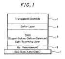
- Fig. 1 shows a basic structure of a thin-film solar cell manufactured from a general chalcopyrite compound semiconductor, which comprises a SLG (soda lime glass) substrate 1 on which a back molybdenum (Mo) electrode layer (positive electrode) 2, a light absorbing layer 5, a buffer layer 6 (ZnS, Cds, etc.) and a transparent electrode layer (negative electrode) 7 made of ZnO, Al, etc are subsequently formed in the described order.
- SLG sina lime glass
- the light absorbing layer 4 is made in the form of a CIGS (Copper-Indium-Gallium-Selenium) thin film made of Cu(In,Ga)Se2 of Ib-IIIb-VIb2 group (based on Cu, (In,Ga), Se), which possesses high power conversion efficiency exceeding 18%.
- CIGS Copper-Indium-Gallium-Selenium
- U.S. Patent No.4798660 discloses a method whereby a thin metal film formed of a metal back-electrode layer, a pure copper (Cu) single layer and a pure indium (In) single layer subsequently deposited by a DC magnetron sputtering method is selenized in a selenium (Se) atmosphere (preferably in H2Se gas) to produce a light absorbing layer having a homogeneous composition of CIS (copper indium diselenium).
- a selenium (Se) atmosphere preferably in H2Se gas
- Japanese Laid-Open Patent Publication No. H10-135495 describes a metal precursor which is a thin metal laminate formed by sputtering first with a target of Cu-Ga alloy and then with a target of pure indium. As shown in Fig. 2, a thin firm of CIGS for a light absorbing layer 4 is formed on a Mo electrode layer 2 deposited on a SLG (soda lime glass) substrate 1.
- a Cu-Ga metal thin layer 31 is first deposited on the Mo-electrode layer of the substrate by the first sputtering process SPT-1 using the Cu-Ga alloy target and then an In metal thin layer 32 is deposited on the Cu-Ga layer 31 by the second sputtering process SPT-2 using the In target T2 to produce a metal-laminated precursor 3 which is then treated by heat in the presence of Selenium (Se) gas by a heat treatment process HEAT to obtain a light absorbing film 5 in the form of a thin CIGS film.
- Selenium (Se) gas by a heat treatment process HEAT to obtain a light absorbing film 5 in the form of a thin CIGS film.
- this precursor 3 being a laminate of a Cu-Ga alloy layer 31 and an In layer 32 may be subjected to solid-state (interlayer) diffusion of elements which react with one another to form an alloy Cu-In-Ga at a boundary between the laminated layers both in process of forming the precursor and in the state of being temporarily stored.
- This reaction still progresses during the selenization of the precursor.
- the quality of the light absorbing layers 5 may considerably vary. The aggregation of indium is apt to occur, resulting in uneven composition in the layer.
- the concentration of Ga in the precursor has a gradient of Mo, which may decrease in the direction toward the surface from the boundary with the Mo electrode layer 2.
- the conventional method still involves a problem that elements Ga segregate on the boundary between the Mo electrode layer 2 and the Cu-In-Ga layer, causing insufficient adhesion between the light absorbing layer 5 of CIGS and the Mo electrode layer 3. This may be a cause of degradation of the performance of the solar cell product.
- a CIGS film deposited on the glass containing Na has a small resistance
- a solar cell produced by forming CIGS on a Na2O2 film preformed on a substrate can attain power conversion efficiency improved by about 2% as compared with that of a solar cell manufactured without deposition of a Na2O2 film and its power conversion efficiency that generally depends largely on the Cu-to-In ratio can be constant irrespective of the Cu-to-In ratio (M. Ruckh et al., "Influence of Substrates on the Electrical Properties of Thin film of Cu(In,Gs)Se2").
- the diffusion or addition of Na is effective to promote the growth of the CuInSw2 film, increase the carrier concentration and improve the power conversion efficiency of the solar cell.
- Japanese Laid-Open Patent Publication No. H8-222750 discloses as a method of doping Na in the process of selenizing a laminated precursor formed after preparation of a Na layer by sputtering or depositing.
- the problem of this process is that a layer of Na or Na compound possessing the hydroscopic property may be denatured by opposing to atmosphere, resulting in peeping of the layer in the precursor.
- US patent No. 5422304 discloses a deposition method of manufacturing the CuInSe2 film by doping Na together with other elements composing the light absorbing layer.
- a method of depositing a Cu-In-O:Na2O2 by sputtering on the Mo electrode layer is also disclosed.
- these methods require rather complicated processes.
- the method of improving the power conversion efficiency of the solar cell by diffusing Na in the light absorbing layer involves a problem of peeling of the Na layer by denature.
- an object of the present invention is to provide a method of forming a CIGS light absorbing layer of a thin-film compound semiconductor solar cell by first forming a precursor film on a back electrode and then treating by heat the precursor film in the presence of selenium to produce the thin-film light absorbing layer of CGIS, wherein an alkali layer for diffusing alkali components of Ia group in the light absorbing layer to increase the power conversion efficiency of the solar cell product is formed by a simple process with no fear of occurrence of denature and peeling of the layer, which process comprises dipping of the back electrode in an alkali aqueous solution containing alkali metals and drying of the dipped electrode to form an alkali layer thereon.
- a light absorbing layer is fabricated by the following process:
- Step S1 On a SLG (soda lime glass) substrate 1, there is first formed by a CVD method a barrier layer 8 of SiO2 for preventing diffusion of Na components from the substrate (Step S1).
- a molybdenum (Mo) electrode layer is next formed on the barrier layer 8 by a sputtering method (Step S2) and an alkali layer 9 of Na2S is then formed on the Mo electrode layer 8 by a dipping method (Step S3).
- the alkali layer 9 is formed for example by dipping the Mo electrode layer 2 formed on the substrate in an aqueous solution prepared by dissolving Na2S ⁇ 9H2O (sodium sulfide) into pure water in a concentration within 0.1-5 wt%.
- the dipped layer is spin-dried and treated by baking at 150°C for 60 minutes in the surrounding air for regulating moisture remaining in the film.
- an indium (In) layer 41 is formed on the alkali layer 9 by the first sputtering process SPT-1 using a single In target T1 and a copper-gallium (Cu-Ga) alloy layer 42 is formed thereon by the second sputtering process SPT-2 using a Cu-Ga alloy target T2 to form a laminated metal precursor 3 composed of the In layer 41 and the Cu-Ga alloy layer 42, which precursor 4 is then treated by heat in the atmosphere of selenium (Se) to form a thin film light absorbing layer 5 of CIGS.
- the alkali layer 9 disappeared by diffusing its components Na into the light absorbing layer 5.
- the present invention it is possible to fabricate a light absorbing layer 5 of CIGS thin film having higher power conversion efficiency, which improvement is achieved by effective diffusion of Na of the alkali layer 9 into the laminated precursor 4 in the process of heat treatment thereof in the presence of selenium. It is also possible to easily obtain an alkali layer 9 by a simple process.
- the alkali film 9 formed by a wet treatment process on the Mo electrode layer 2 contains moisture and can therefore be free from such troubles that a dry film formed by dry process may absorb moisture from the surrounding air resulting in deterioration and peeling of the layer.
- the hydration enables the alkali film to keep moisture which content can be regulated by the baking treatment of the precursor.
- the formed film has excellent wettability.
- aqueous solution of Na2S ⁇ 9H2O which concentration was adjusted in a range of 11 to 13 pH can effectively remove by etching an oxide coat from the Mo electrode layer 2 and at the same time can improve adhesion between surfaces of the Mo electrode layer 2 and the light absorbing layer 5 by the effect of S component.
- Dipping the electrode layer 2 in aqueous solution of alkali metal can remove particles and oxide films by etching from the Mo electrode layer 2. As the result of this, it becomes possible to omit the washing process of the surface of the Mo electrode layer after scribing it by a laser beam.
- the pH of the dipping solution can be easily regulated by adding thereto ammonium or NaOH.
- the use of the aqueous dipping solution makes the alkali layer 9 contain therein, besides hydrogen, residual oxygen which is then incorporated into the light absorbing layer 5, thereby improving the semiconductor properties.
- the buffer layer 8 is provided between the SLG substrate 1 and the Mo electrode layer 2, which can effectively prevent diffusion of Na elements into the light absorbing layer 5 from the substrate 1 through the Mo electrode layer 2 in the process of heat treatment of the light absorbing layer. This can prevent the excessive supply of Na into the light absorbing layer 5 and, at the same time, can effectively prevent deterioration of the substrate 1.
- the measurement results of deposition amount of Na by forming the alkali layer 9 on the Mo electrode layer 2 are as follows:
- concentrations of the aqueous solution of Na2S are suitable in the range of 0.01 to 1.0(5) from the view point of the power conversion efficiency ⁇ .
- the power conversion efficiency ⁇ of the product is decreased with the smaller concentration of the aqueous solution of Na2S.
- the use of the solution of excessively high concentration of Na2S may cause peeling of a layer part by etching at the boundary between the Mo electrode layer 2 and the SLD substrate 1.
- the working temperature of the aqueous solution of Na2S is suitable in a range of 10°C to 70°C (preferably in the range of 15°C to 40°C) from the view point of the power conversion efficiency ⁇ .
- dipping in the solution at lower temperature may cause decreasing of the power conversion efficiency ⁇ of the product while dipping in the solution at temperature of 80°C or higher may cause may cause peeling of a layer part by etching at the boundary between the Mo electrode layer 2 and the SLG substrate 1.
- the baking treatment temperature is suitable in the range of 100°C to 400°C (preferably in the range of 100°C to 250°C) from the view point of the power conversion efficiency ⁇ .
- baking treatment at a lower temperature may cause decreasing of the power conversion efficiency ⁇ of the product while baking treatment at a higher temperature may cause may decrease moisture in the Mo electrode layer 2 which in this case may peel off.
- the measurement results indicate that the baking treatment time is suitable within 10 - 60 minutes from the view point of securing the power conversion efficiency ⁇ and working condition.
- aqueous solutions of alkali metals other than the hydrate of Na2S ⁇ 9H2O or aqueous solutions of sulfide or hydride or chloride of the other alkali metals can be used.
- Na compounds Na2SeO3 ⁇ 5H2O, Na2TeO3 ⁇ 5H2O, Na2SO3 ⁇ 7H2O, Na2B4O7 ⁇ 10H2O, AlNa(SO4)2 ⁇ 12H2O and NaCl.
- K compounds K2TeO3 ⁇ 3H2O, K2Al2O4 ⁇ 3H2O, AlK(SO4)2 ⁇ 12H2O, KOH, KF, K2SeO3, K2TeO3, KCL, K2[CuCl4(H2O)2], KBr, KBH4, K2S2O3 ⁇ nH2O, K2S2O5, K2S2O7, KF ⁇ 2H2O, KF ⁇ HF, K2TiF6, K2B4O7 ⁇ 4H2O, KHSO4 and KI.
- Li compounds Li2B4O7 ⁇ 3H2O, Li2B4O7, LiCl, LiBr, LiBr ⁇ H2O, LiOH, LiOH ⁇ H2O, LiF and Li2SO4 ⁇ H2O.
- a laminated precursor 4 is fabricated by successively forming an In layer 41 and a Cu-Ga alloy layer 42 formed first on a Mo electrode layer 2, thereby preventing the formation of an alloy of elements Cu slowly diffused and segregated in solid phase at a boundary between the precursor and the Mo electrode layer 2.
- This can also facilitate In component to sufficiently diffuse in the precursor on the Mo electrode layer side in the process of selenizing the laminated precursor 4 by heating in the selenium atmosphere, simultaneously preventing slowly diffusing elements Ca from segregating at the boundary of the Mo electrode layer 2 and forming thereat a different alloy layer of Cu-Ga-Se which is inferior in its crystal structure.
- the CIGS light absorbing layer 5 thus fabricated can possess high quality P-type semiconductor structure featured by the homogeneous crystal structure of Cu(In+Ga)Se.
- the present invention it is possible to produce a solar cell which is featured by high performance and high strength of adhesion between the Mo electrode layer 2 and the light absorbing layer 2 and which is free from the formation of a strange layer (Cu-Ga-Se layer) having inferior crystal structure and possessing conductivity.
- Fig. 9 illustrates a laminated precursor 4' according to the present invention, which has a Cu-Ga alloy layer 42 sandwiched between two In layers 41 and 43 and which is formed by sputtering on an alkali layer 9 of Na2S formed on a Mo electrode layer 2. Since the Cu-Ga alloy layer 42 is deposited on the In layer 41 formed in advance on the Mo electrode layer 2, there is no fear of forming of an alloy layer of elements diffused in solid layer at the boundary of the Mo electrode layer 2.
- This structure attains effective diffusion of In-elements in the precursor on the Mo electrode layer side in the process of selenizing the precursor 4' in a selenium (Se) atmosphere, simultaneously eliminating the possibility of segregation of slow diffusing elements Cu at a boundary of the Mo electrode layer and formation thereat of a different alloy layer of Cu-Ga-Se which may have inferior crystal structure.
- the precursor is covered at its top surface with the In layer 43 which eliminates the possibility of forming an alloy of Cu2Se on the surface of the light absorbing layer 5 in the process of selenizing the precursor.
- a CIGS light absorbing layer 5 made of high quality P-type semiconductor of Cu (In+Ga) having higher homogeneity of crystals eliminating the possibility of forming a different layer (Cu-Ga-se) being inferior and fragile in crystal structure and having conductivity at a boundary between the Mo electrode layer 2 and the light absorbing layer 5 and forming a different conductive film (Cu2Se) on the surface of the light absorbing layer 5.
- a solar cell having high quality storage property with no leak can be obtained, which is durable in construction and tight in adhesion of the light absorbing layer to the Mo electrode layer.
- Fig. 10 illustrates another laminated precursor 4" according to the present invention, which has a plurality of Cu-Ga layers each sandwiched between In layers and stacked in stages on a Mo electrode layer.
- a laminated precursor 4" of three-staged structure is fabricated by successively forming an In layer 41, a Cu-Ga alloy layer 42, an In layer 43, a Cu-Ga alloy layer 44, an In layer 45, a Cu-Ga alloy layer 46 and an In layer 43 in the described order on the Mo electrode layer 2.
- the use of the precursor 4" having the bottom In-layer on the Mo-electrode layer 41 and the top In-layer 47, in which the Cu-Ga alloy layer 42, the In layer 43, the Cu-Ga layer 44, the In layer 45 and the Cu-Ga alloy layer 46 are evenly arranged, can produce a CIGS light absorbing layer 5 of a high quality P-type semiconductor made of Cu (In+Ga) having higher homogeneity of crystals.
- Fig. 11 illustrates another process of producing a light absorbing layer according to the present invention, whereby a single-layered precursor film is formed by depositing a mixture of particles Ib group metal element and IIIb group metal element supplied at the same time and then treated by heat in a selenium atmosphere to complete a light absorbing layer of CIGS for a thin film compound semiconductor solar cell.
- the process comprises a sputtering process FT-SPT of preparing a single-layered precursor film 10 on an alkali layer 9 formed in advance on a Mo-electrode layer 2 by depositing thereon a mixture of particles sputtered at the same time from a pair of a copper-gallium (Cu-Ga) target T1 and an indium (In) target T2, disposed opposite to each other, and a heat treatment process HEAT of treating by heat the precursor film deposited on the Mo layer of the SLG substrate 1 in a selenium atmosphere to complete the light absorbing layer 4 of CIGS.
- a sputtering process FT-SPT of preparing a single-layered precursor film 10 on an alkali layer 9 formed in advance on a Mo-electrode layer 2 by depositing thereon a mixture of particles sputtered at the same time from a pair of a copper-gallium (Cu-Ga) target T1 and an indium (In) target T2, disposed opposite to each other,
- the Mo electrode layer 2 in the shown case is formed directly on the SLG substrate 1, it is of course possible to provide between them a barrier layer to prevent the diffusion of Na from the substrate into the Mo electrode layer.
- Fig. 12 illustrates the state of particles sputtered from the Cu-GA target T1 and the In target T2 when forming a precursor film 10 of mixed particles of Cu-GA-In.
- a part of particles sputtered from each of targets T1 (Cu-Ga) and T2 (In) may not be directed to the opposite target and may be directly deposited on the substrate but it amounts very small because particles may be sputtered at such angles at a very small probability.
- Most particles of three kinds of metal elements (Cu, Ga and In) are deposited in well mixed state on the electrode layer formed on the substrate.
- the metal precursor 3 obtained by the method according to the present invention is composed of well mixed particles Cu-AG-In deposited in a single layer whereas the metal cursor obtained by the previously described method are laminated of a thin layer of Cu-Ga and a thin layer of In.
- the metal precursor film 10 of the present invention is featured by higher uniformity of distribution therein of metal elements Cu, Ga and In, thereby preventing the progress of forming an alloy by diffusion of metal elements in solid layers.
- the precursor film 10 thus obtained can be evenly selenized by the proceeding heat treatment process.
- the precursor thus formed and treated by heat to form the light absorbing layer can also prevent the occurrence of a strange crystal layer (different from the crystal structure to be expected) in the thin film compound semiconductor solar cell (final product), which is one of causes of deterioration of the solar cell.
- the metal precursor has a pseudo amorphous structure which is effective to achieve a high quality of a thin CISG film of the light absorbing layer.
- the metal precursor film 10 is an alloy composed of three metal elements, which can prevent the solar cell product from being short-circuited.
- the above-described simultaneous sputtering of both targets T1 and T2 makes it possible to form the precursor film 10 at a high speed.
- the precursor thus formed in a single thin layer composed of three metals (Cu, Ga, In) uniformly distributed therein is then treated by heat in the presence of selenium (Se) to form a selenized thin-film of Cu(In+Ga)Se2, which is a light-absorbing layer (p-type semiconductor) 5 possessing a high quality.
- the light-absorbing layer 5 formed by selenizing the thus prepared precursor film 10 has been proved to show a photoelectric conversion efficiency exceeding 15%.
- Fig. 13 shows an example of a heating temperature characteristic of a furnace wherein the precursor film 10 (the laminated precursor 4) is treated by heat with H2Se gas (diluted with 5% argon gas) to form a CIGS thin film light-absorbing layer 5 by thermal chemical reaction with selenium (in gas phase).
- H2Se gas diluted with 5% argon gas
- the furnace is first heated up to 100°C following by holding for 10 minutes for stabilizing the inside temperature of the furnace.
- the inside temperature is then increased gradually through a stable ramp-up period of about 30 minutes to 500 ⁇ 520°C at which the soda-lime glass (SLG) substrate with a precursor formed thereon may not be deformed and can be heat-treated to obtain the high quality crystal structure of the precursor.
- SSG soda-lime glass
- selenium (Se) produced by thermal decomposition of H2Se gas is supplied from the time t1 when the inside temperature of the furnace reached to 230 ⁇ 250°C.
- the precursor of the substrate is treated for 40 minutes maintaining the furnace inside temperature at 500 to 520°C.
- the furnace is charged with H2Se gas at a normal temperature from the time point when the inside temperature reached 100°C.
- the precursor is treated by heat at a constant inside pressure of the furnace.
- the furnace gas is replaced by argon gas at a low pressure of about 100 Pa to prevent further unnecessary deposition of selenium.
- paired opposite targets not limited to a combination of Cu-Ga and In targets, other combinations of Cu-Ga or Cu-Al and In-Cu, Cu and In or Al, and Cu and In-Cu.
- paired opposite targets not limited to a combination of Cu-Ga and In targets, other combinations of Cu-Ga or Cu-Al and In-Cu, Cu and In or Al, and Cu and In-Cu.
- an alkali layer 9' of chemical compound of Ia group element (Na) with IIIb group element (B, Al, Ca, In, Ti) e.g., sodium tetraborate (Na2B4O7), is formed by the dipping method on a Mo electrode layer 2 and then an In layer 41 and a Cu-Ga alloy layer 42 are successively formed to prepare a laminated precursor 4 on the alkali layer.
- the precursor 4 is heat-treated in the selenium (Se) atmosphere to produce a CIGS thin film light absorbing layer 5.
- the alkali layer 9' is formed for example by dipping the Mo electrode layer 2 formed on the substrate in an aqueous solution prepared by dissolving in pure water Na2B4O7 ⁇ 10H2O (10 hydrate of sodium tetraborate) in a concentration in a range of 0.1 to 5 wt%.
- the dipped layer is spin-dried and treated by baking at 150°C for 60 minutes in surrounding air for regulating the degree of moisture remaining in the film.
- the alkali layer 9 disappears by diffusing its alkali components (Na) into the light absorbing layer 5.
- the alkali layer 9 can be formed by a simple process. Furthermore, the alkali film 9 formed by the wet treatment process on the Mo electrode layer 2 contains moisture and can be free from such troubles that a dry film formed by a dry process may absorb moisture from the surrounding air with the result of deterioration and peeling of the layer. The hydration enables the alkali film to keep moisture which content can be regulated by the baking treatment of the precursor. Thus, the formed film has excellent wettability.
- the thin film CIGS light absorbing layer 5 produced with use of the alkali layers 9' of sodium tetraborate can achieve higher power conversion efficiency in comparison with the thin film CIGS light absorbing layer 5 produced with use alkali layers of sodium sulfide (Na2S).
- the improvement of power conversion efficiency is due much to improvement of characteristics of FF and Voc which may effect to reduce crystal defects.
- the reason why the sodium tetraborate in comparison with the sodium sulfide can more contribute to improvement of characteristics of the light absorbing layer may be as follows:
- sulfur components may cause defects of Cu2S. These defects may occur by adding sulfur to CIGS irrespective of growing method (MBE: Molecular Beam Epitaxy), resulting in decrease in the power conversion efficiency of the product.
- MBE Molecular Beam Epitaxy
- the sodium tetraborate can be applied as a highly concentrated aqueous solution for dipping treatment as compared with the sodium sulfide aqueous solution.
- the aqueous sodium sulfide solution of high concentration may cause peeling of the formed alkali layer while the aqueous sodium tetraborate solution of the same concentration may not cause peeling of the formed alkali layer.
- the use of the sodium tetraborate solution can improve the adhesion between the Mo electrode layer 2 and the CIGS thin film light absorbing layer 5, attaining the higher power conversion efficiency of the product layer 5.
- the measurement results indicate that the power conversion efficiency of the light absorbing layers with the sodium sulfide layers is 2.0 ⁇ 5.5% and the power conversion efficiency of the light absorbing layers with the sodium tetraborate layers is 5.8 ⁇ 9.0.
- Fig. 15 is a graph showing a power conversion efficiency characteristic ⁇ of a product, which was measured with or without dehydration baking (at 150°C for 60 minutes in air) after dipping by changing the sodium tetraborate concentration (wt.%) of dipping solution.
- • shows data of samples obtained without baking
- ⁇ shows data of samples obtained with baking.
- the experiment results indicate that the power conversion efficiency ⁇ have a peak at the dip concentration of 0.8 to 1.0% and decreases at the dip concentration exceeding the peak range, which decrease might be resulted from mottling occurred when the samples were spin-dried after dipping treatment. However, the samples dipped in the solution having such high concentrations were free from peeling of the layer at the boundary between the Mo electrode layer and the light absorbing layer. Experiment results indicate that the effect of dehydration baking treatment may improve variations in the power conversion efficiency ⁇ at the dip concentration of 1.0% or higher but does not achieve the best power conversion efficiency.
- Fig. 16 is a graph showing power conversion efficiencies ⁇ of products, which were obtained by the experiments by changing kinds of alkali metals of aqueous dipping solutions for forming alkali layers by the dipping method. Three kinds of alkali metals (alkali layer samples) were used:
- the light absorbing layer forming method can produce a thin-film CIGS light-absorbing layer by forming a thin-film precursor on a back electrode for a thin film compound solar cell (final product) and treated by heat in a selenium (Se) atmosphere, wherein the back electrode is dipped in an aqueous solution containing alkali metals and dried to form an alkali layer thereon and the precursor is then formed on the alkali layer.
- This method may easily form a layer of Ia-group alkali metal elements to be diffused in the light absorbing layer to improve the power conversion efficiency without causing peeling of the layer at the boundary of the back electrode layer.
- the application of this process to the production line of thin film solar cells makes it easier to fabricate solar cells which have durable structure and possess higher conversion efficiency.
Landscapes
- Photovoltaic Devices (AREA)
- Physical Deposition Of Substances That Are Components Of Semiconductor Devices (AREA)
Abstract
Description
Three kinds of alkali metals (alkali layer samples) were used:
Claims (12)
- A light absorbing layer producing method for fabricating a light absorbing layer of CIGS by forming a thin-film precursor on a back electrode of a compound semiconductor solar cell and by treating the formed precursor by heat in a selenium atmosphere, wherein an alkali layer is formed on the back electrode layer by dipping the back electrode in an aqueous solution containing alkali metals and drying the dipped surface and the precursor is then formed on the alkali layer and treated by heat in a selenium (Se) atmosphere.
- A light absorbing layer producing method as defined in claim 1, wherein the aqueous solution is prepared by solving a hydrate of a compound containing alkali metal.
- A light absorbing layer producing method as defined in claim 1, wherein the aqueous solution contains alkali metal in a concentration range of 0.01 to 1.0%.
- A light absorbing layer producing method as defined in claim 1, wherein the aqueous solution is prepared to have pH capable of removing by etching an oxide film from a surface of the back electrode.
- A light absorbing layer producing method as defined in claim 4, wherein the pH of the aqueous solution is in a range of 11 to 13.
- A light absorbing layer producing method as defined in claim 4, wherein a temperature of the aqueous solution is in a range of normal temperature to 70°C.
- A light absorbing layer producing method as defined in claim 1, wherein the alkali layer is spin-dried and then baked for regulating moisture remaining therein.
- A light absorbing layer producing method as defined in claim 6, wherein the alkali layer is treated by baking at a temperature of 100 to 350°C for 10 to 60 minutes.
- A light absorbing layer producing method as defined in claim 1, wherein between a glass substrate and the back electrode is provided a barrier layer for stopping diffusion of alkaline components of the glass substrate into the back electrode.
- A light absorbing layer producing method as defined in claim 1, wherein a laminated precursor film composed of an indium (In) layer and a copper-gallium (CU-Ga) alloy layer is formed on the alkali layer by sputtering from an indium (In) target and a copper-gallium (Cu-Ga) alloy target respectively.
- A light absorbing layer producing method as defined in claim 10, wherein the laminated precursor film is formed by first forming an indium (In) layer on the alkali layer and then forming the copper-gallium (Cu-Ga) alloy layer on the indium (In) layer.
- A light absorbing layer producing method as defined in claim 1, wherein a single layered indium-copper--gallium (In-Cu-Ga) alloy precursor film is formed on the alkali layer by opposite sputtering method using an indium (In) target and a copper-gallium (Cu-Ga) target arranged opposite to each other.
Applications Claiming Priority (5)
| Application Number | Priority Date | Filing Date | Title |
|---|---|---|---|
| JP2002079680 | 2002-02-14 | ||
| JP2002079680 | 2002-02-14 | ||
| JP2002383098 | 2002-12-09 | ||
| JP2002383098 | 2002-12-09 | ||
| PCT/JP2003/000792 WO2003069684A1 (en) | 2002-02-14 | 2003-01-28 | Light absorbing layer forming method |
Publications (2)
| Publication Number | Publication Date |
|---|---|
| EP1475841A1 true EP1475841A1 (en) | 2004-11-10 |
| EP1475841A4 EP1475841A4 (en) | 2008-08-27 |
Family
ID=27736590
Family Applications (1)
| Application Number | Title | Priority Date | Filing Date |
|---|---|---|---|
| EP03703062A Withdrawn EP1475841A4 (en) | 2002-02-14 | 2003-01-28 | PROCESS FOR FORMATION OF LAYER REINFORCING LIGHT |
Country Status (5)
| Country | Link |
|---|---|
| US (1) | US7018858B2 (en) |
| EP (1) | EP1475841A4 (en) |
| JP (1) | JP3876440B2 (en) |
| AU (1) | AU2003207295A1 (en) |
| WO (1) | WO2003069684A1 (en) |
Cited By (1)
| Publication number | Priority date | Publication date | Assignee | Title |
|---|---|---|---|---|
| WO2007070880A1 (en) * | 2005-12-15 | 2007-06-21 | University Of Delaware | Post-deposition treatments of electrodeposited cu(in-ga)se2-based thin films |
Families Citing this family (52)
| Publication number | Priority date | Publication date | Assignee | Title |
|---|---|---|---|---|
| EP1556902A4 (en) | 2002-09-30 | 2009-07-29 | Miasole | APPARATUS AND METHOD FOR MANUFACTURING CON CURRENT FOR LARGE SCALE PRODUCTION OF THIN FILM SOLAR CELLS |
| CN101894881A (en) * | 2004-03-15 | 2010-11-24 | 索罗能源公司 | Technique and apparatus for depositing thin semiconductor layers for solar cell manufacture |
| US7736940B2 (en) | 2004-03-15 | 2010-06-15 | Solopower, Inc. | Technique and apparatus for depositing layers of semiconductors for solar cell and module fabrication |
| US7871502B2 (en) * | 2004-05-11 | 2011-01-18 | Honda Motor Co., Ltd. | Method for manufacturing chalcopyrite thin-film solar cell |
| CN100418235C (en) * | 2005-06-03 | 2008-09-10 | 清华大学 | Preparation method of copper gallium alloy target for copper indium gallium selenide thin film solar cell |
| US7833821B2 (en) * | 2005-10-24 | 2010-11-16 | Solopower, Inc. | Method and apparatus for thin film solar cell manufacturing |
| US20070093006A1 (en) * | 2005-10-24 | 2007-04-26 | Basol Bulent M | Technique For Preparing Precursor Films And Compound Layers For Thin Film Solar Cell Fabrication And Apparatus Corresponding Thereto |
| US8389852B2 (en) * | 2006-02-22 | 2013-03-05 | Guardian Industries Corp. | Electrode structure for use in electronic device and method of making same |
| US20070240758A1 (en) * | 2006-04-14 | 2007-10-18 | Thomas Spartz | Double-sided solar module |
| EP2944383A3 (en) * | 2006-11-09 | 2016-02-10 | Alliance for Sustainable Energy, LLC | Precursors for formation of copper selenide, indium selenide, copper indium diselenide, and/or copper indium gallium diselenide films |
| US20080169025A1 (en) * | 2006-12-08 | 2008-07-17 | Basol Bulent M | Doping techniques for group ibiiiavia compound layers |
| JP4304638B2 (en) * | 2007-07-13 | 2009-07-29 | オムロン株式会社 | CIS solar cell and manufacturing method thereof |
| JP4974986B2 (en) | 2007-09-28 | 2012-07-11 | 富士フイルム株式会社 | Solar cell substrate and solar cell |
| JP2009267336A (en) | 2007-09-28 | 2009-11-12 | Fujifilm Corp | Substrate for solar cell and solar cell |
| US8771419B2 (en) * | 2007-10-05 | 2014-07-08 | Solopower Systems, Inc. | Roll to roll evaporation tool for solar absorber precursor formation |
| US8613973B2 (en) | 2007-12-06 | 2013-12-24 | International Business Machines Corporation | Photovoltaic device with solution-processed chalcogenide absorber layer |
| AT10578U1 (en) * | 2007-12-18 | 2009-06-15 | Plansee Metall Gmbh | DUNGOUS SOLAR CELL WITH MOLYBDAN-CONTAINING ELECTRODE LAYER |
| US7842534B2 (en) * | 2008-04-02 | 2010-11-30 | Sunlight Photonics Inc. | Method for forming a compound semi-conductor thin-film |
| WO2010032803A1 (en) * | 2008-09-18 | 2010-03-25 | 富士フイルム株式会社 | Substrate for solar cell, and solar cell |
| US8425739B1 (en) * | 2008-09-30 | 2013-04-23 | Stion Corporation | In chamber sodium doping process and system for large scale cigs based thin film photovoltaic materials |
| JP5229901B2 (en) * | 2009-03-09 | 2013-07-03 | 富士フイルム株式会社 | Photoelectric conversion element and solar cell |
| US8709856B2 (en) * | 2009-03-09 | 2014-04-29 | Zetta Research and Development LLC—AQT Series | Enhancement of semiconducting photovoltaic absorbers by the addition of alkali salts through solution coating techniques |
| JP5498221B2 (en) | 2009-04-08 | 2014-05-21 | 富士フイルム株式会社 | Semiconductor device and solar cell using the same |
| TW201042065A (en) * | 2009-05-22 | 2010-12-01 | Ind Tech Res Inst | Methods for fabricating copper indium gallium diselenide (CIGS) compound thin films |
| WO2010141463A1 (en) * | 2009-06-04 | 2010-12-09 | First Solar, Inc. | Dopant-containing contact material |
| KR101072089B1 (en) * | 2009-09-30 | 2011-10-10 | 엘지이노텍 주식회사 | Solar cell and method of fabircating the same |
| JP2011097041A (en) * | 2009-10-02 | 2011-05-12 | Showa Denko Kk | Manufacturing method of semiconductor element |
| KR20110060139A (en) * | 2009-11-30 | 2011-06-08 | 삼성전자주식회사 | Solar cell manufacturing method |
| US8501524B2 (en) * | 2010-02-26 | 2013-08-06 | Electronics And Telecommunications Research Institute | Method of manufacturing thin-film light-absorbing layer, and method of manufacturing thin-film solar cell using the same |
| CN102782853A (en) * | 2010-03-05 | 2012-11-14 | 第一太阳能有限公司 | Photovoltaic device with graded buffer layer |
| JP5389253B2 (en) * | 2010-03-05 | 2014-01-15 | 株式会社東芝 | Compound thin film solar cell and manufacturing method thereof |
| WO2011146115A1 (en) | 2010-05-21 | 2011-11-24 | Heliovolt Corporation | Liquid precursor for deposition of copper selenide and method of preparing the same |
| KR20110128580A (en) | 2010-05-24 | 2011-11-30 | 삼성전자주식회사 | Solar cell manufacturing method |
| US8772826B2 (en) * | 2010-05-31 | 2014-07-08 | Kyocera Corporation | Photoelectric conversion device |
| CN102315294A (en) * | 2010-07-05 | 2012-01-11 | 冠晶光电股份有限公司 | CIGS solar cell and method for manufacturing same |
| TWI422045B (en) * | 2010-07-08 | 2014-01-01 | Gcsol Tech Co Ltd | CIGS solar cell process equipment and method |
| US9142408B2 (en) | 2010-08-16 | 2015-09-22 | Alliance For Sustainable Energy, Llc | Liquid precursor for deposition of indium selenide and method of preparing the same |
| US8048707B1 (en) * | 2010-10-19 | 2011-11-01 | Miasole | Sulfur salt containing CIG targets, methods of making and methods of use thereof |
| WO2012098722A1 (en) | 2011-01-17 | 2012-07-26 | Jx日鉱日石金属株式会社 | Cu-ga target and method for manufacturing same, as well as light-absorbing layer formed from cu-ga alloy film, and cigs solar cell using light-absorbing layer |
| JP5620334B2 (en) * | 2011-05-18 | 2014-11-05 | 株式会社神戸製鋼所 | CIGS solar cells |
| WO2012173360A2 (en) * | 2011-06-13 | 2012-12-20 | 주식회사 포스코 | Solar cell substrate and solar cell using same |
| KR101867616B1 (en) * | 2011-12-20 | 2018-06-15 | 주식회사 포스코 | Solar cell having layer for diffusion barrier |
| KR20130105325A (en) * | 2012-03-12 | 2013-09-25 | 한국에너지기술연구원 | Method for preparing cigs-based thin film solar cell using na-free substrate and solar cell prepared by the same |
| US9224903B2 (en) | 2012-04-17 | 2015-12-29 | Kyocera Corporation | Method for manufacturing photoelectric converter |
| US9105797B2 (en) | 2012-05-31 | 2015-08-11 | Alliance For Sustainable Energy, Llc | Liquid precursor inks for deposition of In—Se, Ga—Se and In—Ga—Se |
| US8871560B2 (en) * | 2012-08-09 | 2014-10-28 | International Business Machines Corporation | Plasma annealing of thin film solar cells |
| KR101450426B1 (en) | 2013-01-09 | 2014-10-14 | 연세대학교 산학협력단 | Solution for sodium doping to fabricate high quality chalcogenide absorber layer and method for thin film solar cell using the same |
| JP6451059B2 (en) * | 2014-02-28 | 2019-01-16 | セイコーエプソン株式会社 | Photoelectric conversion device, method for manufacturing photoelectric conversion device, and electronic apparatus |
| CN105070784A (en) * | 2015-07-17 | 2015-11-18 | 邓杨 | New, cheap and efficient CIGS cell absorbent layer preparation process |
| US10727366B2 (en) * | 2016-01-13 | 2020-07-28 | Mecaroenergy Co., Ltd. | Solar cell comprising CIGS light absorbing layer and method for manufacturing same |
| CN105870255B (en) * | 2016-04-27 | 2017-04-05 | 河南大学 | A kind of method that cosputtering method prepares CIGS thin film solar battery obsorbing layer |
| CN108198892A (en) * | 2017-12-22 | 2018-06-22 | 兰州空间技术物理研究所 | A kind of preparation method for mixing potassium flexible copper indium gallium selenide thin-film solar cell |
Family Cites Families (12)
| Publication number | Priority date | Publication date | Assignee | Title |
|---|---|---|---|---|
| US4945079A (en) * | 1984-11-13 | 1990-07-31 | Aluminum Company Of America | Catalyst of nickel and molybdenum supported on alumina |
| US4798660A (en) | 1985-07-16 | 1989-01-17 | Atlantic Richfield Company | Method for forming Cu In Se2 films |
| JPH05262504A (en) | 1991-09-27 | 1993-10-12 | Matsushita Electric Ind Co Ltd | Compound semiconductor, production of its thin film and semiconductor device using the same |
| CH687112A5 (en) * | 1993-06-08 | 1996-09-13 | Yazaki Corp | A method for depositing a precursor of CuInSe compound (2). |
| SE508676C2 (en) * | 1994-10-21 | 1998-10-26 | Nordic Solar Energy Ab | Process for making thin film solar cells |
| DE4442824C1 (en) * | 1994-12-01 | 1996-01-25 | Siemens Ag | Solar cell having higher degree of activity |
| JP3249408B2 (en) | 1996-10-25 | 2002-01-21 | 昭和シェル石油株式会社 | Method and apparatus for manufacturing thin film light absorbing layer of thin film solar cell |
| JP3327811B2 (en) * | 1997-05-13 | 2002-09-24 | キヤノン株式会社 | Method for producing zinc oxide thin film, photovoltaic element and semiconductor element substrate using the same |
| JPH11274534A (en) * | 1998-03-25 | 1999-10-08 | Yazaki Corp | I-III-VI group compound semiconductor and thin film solar cell using the same |
| JP2000174306A (en) * | 1998-12-01 | 2000-06-23 | Asahi Chem Ind Co Ltd | Manufacture of compound semiconductor thin film |
| JP3503824B2 (en) * | 2000-03-23 | 2004-03-08 | 松下電器産業株式会社 | Solar cell and method for manufacturing the same |
| JP3696156B2 (en) * | 2000-12-26 | 2005-09-14 | 株式会社東芝 | Coating film heating apparatus and resist film processing method |
-
2003
- 2003-01-28 WO PCT/JP2003/000792 patent/WO2003069684A1/en not_active Ceased
- 2003-01-28 EP EP03703062A patent/EP1475841A4/en not_active Withdrawn
- 2003-01-28 AU AU2003207295A patent/AU2003207295A1/en not_active Abandoned
- 2003-01-28 JP JP2003568702A patent/JP3876440B2/en not_active Expired - Fee Related
-
2004
- 2004-06-18 US US10/871,450 patent/US7018858B2/en not_active Expired - Fee Related
Cited By (1)
| Publication number | Priority date | Publication date | Assignee | Title |
|---|---|---|---|---|
| WO2007070880A1 (en) * | 2005-12-15 | 2007-06-21 | University Of Delaware | Post-deposition treatments of electrodeposited cu(in-ga)se2-based thin films |
Also Published As
| Publication number | Publication date |
|---|---|
| EP1475841A4 (en) | 2008-08-27 |
| JP3876440B2 (en) | 2007-01-31 |
| JPWO2003069684A1 (en) | 2005-06-09 |
| US20050028861A1 (en) | 2005-02-10 |
| US7018858B2 (en) | 2006-03-28 |
| AU2003207295A1 (en) | 2003-09-04 |
| WO2003069684A1 (en) | 2003-08-21 |
Similar Documents
| Publication | Publication Date | Title |
|---|---|---|
| US7018858B2 (en) | Light absorbing layer producing method | |
| Wang | Progress in thin film solar cells based on Cu2ZnSnS4 | |
| JP4110515B2 (en) | Thin film solar cell and manufacturing method thereof | |
| TWI554624B (en) | Sodium sputtering doping method for large-scale CIGS-based thin film photovoltaic materials | |
| Li et al. | CZTSSe solar cells: insights into interface engineering | |
| US5112410A (en) | Cadmium zinc sulfide by solution growth | |
| US20070257255A1 (en) | Thin film solar cells by selenization sulfurization using diethyl selenium as a selenium precursor | |
| KR20090106513A (en) | Doping Techniques for Group IVIIIIIAVIA Compound Layers | |
| CA2586963A1 (en) | Process and photovoltaic device using an akali-containing layer | |
| Baid et al. | A comprehensive review on Cu2ZnSnS4 (CZTS) thin film for solar cell: forecast issues and future anticipation | |
| KR102594725B1 (en) | Post-processing method of absorber layer | |
| JP6510529B2 (en) | Thin film solar cell, layer system for thin film solar cell and method for producing layer system for thin film solar cell | |
| US20100248417A1 (en) | Method for producing chalcopyrite-type solar cell | |
| Saha | A Status Review on Cu2ZnSn (S, Se) 4‐Based Thin‐Film Solar Cells | |
| JP2004047916A (en) | Compound thin-film solar cell and method of manufacturing the same | |
| TWI587532B (en) | Method for manufacturing photovoltaic device, method and system for processing absorption layer | |
| JP4055064B2 (en) | Method for manufacturing thin film solar cell | |
| US20120322198A1 (en) | METHODS FOR SUBLIMATION OF Mg AND INCORPORATION INTO CdTe FILMS TO FORM TERNARY COMPOSITIONS | |
| KR20180034248A (en) | Flexible CZTS-based thin film solar cell using sodium hydroxide and manufacturing method thereof | |
| KR102584673B1 (en) | Flexible thin film solar cell and method for manufacturing the same | |
| US20250063848A1 (en) | Cadmium Selenide Based Photovoltaic Devices And Methods For Forming The Same | |
| JP2003258282A (en) | Manufacturing method of light absorbing layer | |
| JP2019071342A (en) | Method of manufacturing thin film solar cell | |
| KR102596328B1 (en) | Preparation method for CZTS thin film solar cell absorbing layer, CZTS thin film solar cell absorbing layer prepared therefrom | |
| WO2013160356A1 (en) | Method for manufacturing a semiconductor thin film |
Legal Events
| Date | Code | Title | Description |
|---|---|---|---|
| PUAI | Public reference made under article 153(3) epc to a published international application that has entered the european phase |
Free format text: ORIGINAL CODE: 0009012 |
|
| 17P | Request for examination filed |
Effective date: 20040408 |
|
| AK | Designated contracting states |
Kind code of ref document: A1 Designated state(s): AT BE BG CH CY CZ DE DK EE ES FI FR GB GR HU IE IT LI LU MC NL PT SE SI SK TR |
|
| AX | Request for extension of the european patent |
Extension state: AL LT LV MK RO |
|
| A4 | Supplementary search report drawn up and despatched |
Effective date: 20080729 |
|
| RIC1 | Information provided on ipc code assigned before grant |
Ipc: H01L 31/0336 20060101ALI20080724BHEP Ipc: H01L 31/032 20060101AFI20080724BHEP |
|
| 17Q | First examination report despatched |
Effective date: 20081215 |
|
| GRAP | Despatch of communication of intention to grant a patent |
Free format text: ORIGINAL CODE: EPIDOSNIGR1 |
|
| RIC1 | Information provided on ipc code assigned before grant |
Ipc: H01L 31/18 20060101AFI20180201BHEP Ipc: H01L 31/032 20060101ALI20180201BHEP Ipc: H01L 31/0749 20120101ALI20180201BHEP |
|
| INTG | Intention to grant announced |
Effective date: 20180226 |
|
| STAA | Information on the status of an ep patent application or granted ep patent |
Free format text: STATUS: THE APPLICATION IS DEEMED TO BE WITHDRAWN |
|
| 18D | Application deemed to be withdrawn |
Effective date: 20180710 |
|
| RIC1 | Information provided on ipc code assigned before grant |
Ipc: H01L 31/18 20060101AFI20180201BHEP Ipc: H01L 31/032 20060101ALI20180201BHEP Ipc: H01L 31/0749 20120101ALI20180201BHEP |