JP4055064B2 - Method for manufacturing thin film solar cell - Google Patents
Method for manufacturing thin film solar cell Download PDFInfo
- Publication number
- JP4055064B2 JP4055064B2 JP2002337272A JP2002337272A JP4055064B2 JP 4055064 B2 JP4055064 B2 JP 4055064B2 JP 2002337272 A JP2002337272 A JP 2002337272A JP 2002337272 A JP2002337272 A JP 2002337272A JP 4055064 B2 JP4055064 B2 JP 4055064B2
- Authority
- JP
- Japan
- Prior art keywords
- layer
- electrode layer
- substrate
- light absorption
- alkali
- Prior art date
- Legal status (The legal status is an assumption and is not a legal conclusion. Google has not performed a legal analysis and makes no representation as to the accuracy of the status listed.)
- Expired - Fee Related
Links
Images


Classifications
-
- Y—GENERAL TAGGING OF NEW TECHNOLOGICAL DEVELOPMENTS; GENERAL TAGGING OF CROSS-SECTIONAL TECHNOLOGIES SPANNING OVER SEVERAL SECTIONS OF THE IPC; TECHNICAL SUBJECTS COVERED BY FORMER USPC CROSS-REFERENCE ART COLLECTIONS [XRACs] AND DIGESTS
- Y02—TECHNOLOGIES OR APPLICATIONS FOR MITIGATION OR ADAPTATION AGAINST CLIMATE CHANGE
- Y02E—REDUCTION OF GREENHOUSE GAS [GHG] EMISSIONS, RELATED TO ENERGY GENERATION, TRANSMISSION OR DISTRIBUTION
- Y02E10/00—Energy generation through renewable energy sources
- Y02E10/50—Photovoltaic [PV] energy
- Y02E10/541—CuInSe2 material PV cells
-
- Y—GENERAL TAGGING OF NEW TECHNOLOGICAL DEVELOPMENTS; GENERAL TAGGING OF CROSS-SECTIONAL TECHNOLOGIES SPANNING OVER SEVERAL SECTIONS OF THE IPC; TECHNICAL SUBJECTS COVERED BY FORMER USPC CROSS-REFERENCE ART COLLECTIONS [XRACs] AND DIGESTS
- Y02—TECHNOLOGIES OR APPLICATIONS FOR MITIGATION OR ADAPTATION AGAINST CLIMATE CHANGE
- Y02P—CLIMATE CHANGE MITIGATION TECHNOLOGIES IN THE PRODUCTION OR PROCESSING OF GOODS
- Y02P70/00—Climate change mitigation technologies in the production process for final industrial or consumer products
- Y02P70/50—Manufacturing or production processes characterised by the final manufactured product
Description
【0001】
【産業上の利用分野】
本発明は、化合物半導体による薄膜太陽電池の製造方法に関する。
【0002】
【従来の技術】
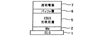
図1は、一般的なカルコパイライト系化合物半導体による薄膜太陽電池の基本構造を示している。それは、SLG(ソーダライムガラス)基板1上に裏面電極(プラス電極)となるMo電極層2が形成され、そのMo電極層2上に光吸収層5が形成され、その光吸収層5上にZnS,CdSなどからなるバッファ層6を介して、マイナス電極となるZnO:Alなどからなる透明電極層7が形成されている。
【0003】
その化合物半導体による薄膜太陽電池における光吸収層4としては、現在18%を超す高いエネルギー変換効率が得られるものとして、Cu,(In,Ga),SeをベースとしたIb−IIIb−VIb2族系のCu(In+Ga)Se2によるCIGS薄膜が用いられている。
【0004】
従来、CIGS薄膜による光吸収層を作製する方法として、金属プリカーサ(前駆体)薄膜を用いて、H2Seガス等のSeソースを用いた熱化学反応でSe化合物を生成するセレン化法がある。
【0005】
米国特許第4798660号明細書には、DCマグネトロンスパッタリング法により、裏面電極層→純Cu単独層→純In単独層の順に積層する構造で形成した金属薄膜層をSe雰囲気、望ましくはH2Seガス中でセレン化することで均一な組成のCIS単相からなる光吸収層を形成することが開示されている。
【0006】
特開平10−135495号明細書には、金属プリカーサとして、Cu−Gaの合金ターゲットを用いてスパッタ成膜された金属薄膜と、Inターゲットを用いてスパッタ成膜された金属薄膜との積層構造によるものが示されている。
【0007】
それは、図2に示すように、SLG(ソーダライムガラス)基板1に成膜されているMo電極層2上にCIGS薄膜による光吸収層5を形成するに際して、先にCu−Gaの合金ターゲットT2を用いた第1のスパッタ工程SPT−1によってCu−Ga合金層31を成膜し、次いで、InターゲットT1を用いた第2のスパッタ工程SPT−2によってIn層32を成膜して、Cu−Ga合金層31、In層32による積層プリカーサ3を形成するようにしている。そして、熱処理工程HEATにおいて、その積層プリカーサ3をSe雰囲気中で熱処理することにより、CIGS薄膜による光吸収層5を作製するようにしている。
【0008】
しかし、Cu−Ga合金層31とIn層32との積層構造によるプリカーサ3を形成するのでは、成膜時やそのストック時に、その積層の界面で固層拡散(固体間の拡散)による合金化反応が進行して、Cu−In−Gaの3元合金が形成されてしまう。また、後で行われるSe化工程においても合金化反応は進行する。この積層プリカーサ3の積層の界面における合金化反応の進行をサンプル間で一様に管理することは難しく(温度や時間等の合金化反応に関与するパラメータの管理が必要となる)、得られる光吸収層5の品質がばらついてしまう。そして、In層32が凝集し、面内での組成不均一が生じやすいものになってしまう。
【0009】
そのため、Ga濃度をMo電極層2との界面から表面に向かって低くなるようにGa濃度勾配をもたせるようにすることが提案されている。
【0010】
しかし、このような従来の光吸収層の形成方法によるのでは、GaがMo電極層2とCu−In−Ga層との界面に偏析するために、Mo電極層2とCIGS薄膜による光吸収層5との密着不良の問題をきたして、電池特性の劣化の要因となっている。
【0011】
また、従来、基板となるソーダライムガラス中のアルカリ金属元素(Na元素)がCuInSe2膜に拡散して粒が成長することが示され、そのアルカリ金属元素が拡散したCuInSe2膜を用いた太陽電池のエネルギー変換効率が高くなることが報告されている(第12回ヨーロッパ光起電力太陽エネルギー会議M.Bodegard等による「THE INFRUENCE OF SODIUM ON THE GRAIN STRUCTURE OF CuInSe2 FILMS FOR PHOTOVOLTAIC APPLICATIONS」)。
【0012】
さらに、アルカリ成分を含むガラス上に堆積したCIGS膜の抵抗値が小さいことと、基板上にNa2O2膜を堆積した後にCIGS膜を形成した太陽電池では、エネルギー変換効率がNa2O2膜を堆積していない太陽電池の約2%向上し、さらに通常Cu/In比に大きく依存するエネルギー変換効率がCu/In比にかかわらず一定になることが報告されている{第1回光起電力エネルギー変換世界会議 M.Ruckh等による「INFRUENCE OF SUBSTRATES ON THE ELECTRICAL PROPERTIES OF Cu(In,Gs)Se2 THINFILMS」}。
【0013】
以上の報告からわかるように、CuInSe2膜の成長の促進とキャリア濃度の増加および太陽電池のエネルギー変換効率の向上にはアルカリ金属元素の拡散あるいは添加が有効である。
【0014】
アルカリ金属元素のドーピング方法として、Mo電極(裏面電極)層上に蒸着法またはスパッタリング法によってアルカリ金属元素を含有するアルカリ層を形成したのちに、積層プリカーサを形成してセレン化する方法が特開平8−222750号明細書に示されている。この製法の課題は、NaまたはNa化合物によるアルカリ層が吸湿性を有しているために、成膜したのち大気にふれると変質しで、その結果剥離してしまうことである。
【0015】
そのため、光吸収層を構成する他の元素と同時にアルカリ金属元素をドーピングする蒸着法によるCuInSe2膜の製法が米国特許第542204号に開示されている。また、Mo電極層上にスパッタリング法によりCu−In−O:Na2O2を堆積する方法が開示されている。しかし、これらの方法では、その作業工程が煩雑になっている。
【0016】
また、その特開平8−222750号明細書には、SLG基板から光吸収層へのアルカリ金属元素の拡散を阻止するために、SLG基板と光吸収層との間にバリア層を設けるか、またはアルカリ金属を含有しない基板を用いることが開示されている。
【0017】
【発明が解決しようとする課題】
解決しようとする問題点は、化合物半導体による薄膜太陽電池における裏面電極層上にCu−Ga合金層およびIn層からなる積層プリカーサ膜を形成して、Se雰囲気中で熱処理することによってCIGS系の光吸収層を作製するに際して、エネルギー変換効率を向上させるために光吸収層にアルカリ金属元素を拡散させるべく、裏面電極層上に蒸着法またはスパッタリング法によってアルカリ層を形成するのでは、成膜されるアルカリ層が変質して剥離しやすいものになってしまうことである。
【0018】
また、積層プリカーサのセレン化時にアルカリ金属元素をドーピングしたり、裏面電極層上にスパッタリング法によりCu−In−O:Na2O2を堆積したうえで、その上に積層プリカーサ膜を形成してセレン化したりするのでは、その作業工程が煩雑になってしまうという問題がある。
【0019】
また、SLG基板と光吸収層との間にSLG基板から光吸収層へのアルカリ金属元素の拡散を阻止するためのバリア層を設けるか、またはアルカリ金属元素を含有しない基板を用いて、裏面電極層上に設けられたアルカリ層から光吸収層へアルカリ金属元素を拡散させるのでは効率が悪いという問題がある。
【0020】
【課題を解決するための手段】
本発明は、基板上に裏面電極層を形成して、その裏面電極層上にプリカーサ膜を形成して、SeまたはS雰囲気中で熱処理することによってCIGS系の光吸収層を作製し、その光吸収層上にバッファ層を介して透明電極層を形成するようにした薄膜太陽電池の製造方法にあって、その熱処理時に効率良く効果的に光吸収層にアルカリ金属元素を拡散させることができるようにするべく、前記基板にアルカリ成分を含む基板を用いるとともに、Ia族元素を含む水溶液に裏面電極層を浸漬したのち乾燥させて裏面電極層上にアルカリ層を形成するようにして、前記熱処理時にその基板およびアルカリ層からそれぞれアルカリ金属元素が光吸収層に拡散するようにしたうえで、前記裏面電極をPVD法にて成膜することにより前記基板からのアルカリ金属元素が光吸収層に拡散する拡散量をPVD法の成膜圧力の変化により膜質を変化させて、前記アルカリ層と前記基板からのアルカリ金属元素が単位面積あたり10E+10〜10E+16の範囲原子数密度をもって光吸収層に拡散されるようにしている。
【0021】
具体的には、裏面電極の膜厚、膜質の適正化を図ることによって、アルカリ金属元素の拡散量を制御することになる。
【0022】
そして、本発明は、アルカリ成分を含む基板上に、基板に対して密着性を確保するための固定の第1の裏面電極層と、アルカリ金属元素の拡散量を制御するための第2の裏面電極層との積層構造による裏面電極を形成するようにしている。
【0023】
また、本発明では、化合物半導体による薄膜太陽電池における裏面電極上にプリカーサ膜を形成して、Se雰囲気中で熱処理することによってCIGS系の光吸収層を作製するに際して、エネルギー変換効率を向上させるために光吸収層にアルカリ金属元素を拡散させる層を、変質や剥離の問題を生ずることなく、簡単な工程で得ることができるようにするべく、Ia族元素を含む水溶液に裏面電極を浸漬したのち乾燥させて裏面電極上にアルカリ層を形成するようにしている。
【0024】
さらに、本発明は、熱処理時に生ずる熱応力によって基板と裏面電極との間が剥離することがないように、基板と裏面電極との間に応力緩和層を設けるようにしている。
【0025】
【実施例】
本発明による薄膜太陽電池の製造方法にあっては、基本的に、図3に示すように、SLG基板1上に、そのSLG基板1に含まれるアルカリ金属元素(Na)拡散量を所定に制御するように膜厚、膜質が適正化されたMo電極層2′をスパッタリング法(またはPVD法)によって形成する(ステップS1)。
【0026】
次いで、そのMo電極層2′上にNa2Sからなるアルカリ層9を浸漬法によって成膜する(ステップS2)。
【0027】
そのアルカリ層9の成膜としては、例えば、Na2S・9H2O(硫化ナトリウム9水和物)を重量濃度0.1〜5%で純水に溶かした水溶液にMo電極層2′の成膜基板を浸して、スピンドライ乾燥させたのち、膜中残留水分の調整のために、大気中、150℃で60分間のベーク処理を行う。
【0028】
次いで、アルカリ層9上に、先にIn単体ターゲットを用いた第1のスパッタリング工程によってIn層41を成膜したうえで(ステップS3)、その上に、Cu−Gaの合金ターゲットを用いた第2のスパッタリング工程によってCu−Ga合金層42を成膜して(ステップS4)、In層41およびCu−Ga合金層42からなる積層プリカーサ4を形成する。
【0029】
そして、図4に示すように、その積層プリカーサ4をSe雰囲気中で熱処理して、CIGS薄膜による光吸収層5′を作製する(ステップS5)。
【0030】
この熱処理時に、SLG基板1からMo電極層2′を通して、そのMo電極層2′によって最適に制御された量のアルカリ金属元素が光吸収層5′に拡散するとともに、アルカリ層9から所定量のアルカリ金属元素が光吸収層5′に拡散する。
【0031】
その際、アルカリ層9は、予め所定量のアルカリ金属元素を供給できる膜質(アルカリ金属元素の含有密度)および膜厚をもって成膜されており、所定量のアルカリ金属元素が光吸収層5′に拡散して消滅する。
【0032】
また、SLG基板1から光吸収層5′に拡散するアルカリ金属元素にあっても、それが過剰に供給されることなく適量となるように、Mo電極層2′の膜質および膜厚が設定されている。
【0033】
スパッタリング法による薄膜の成膜条件(温度、圧力、供給電力等)を変化させることによって、薄膜としての諸特性が変化することが知られている。本発明では、Mo電極層2′の成膜圧力を制御することによって、SLG基板1からMo電極層2′を通して光吸収層5′に拡散するアルカリ金属元素の量が適正になるように調整している。
【0034】
具体的には、単位面積1cm2当り10E+10〜10E+16の範囲の原子数密度をもって、光吸収層5′にアルカリ金属元素が拡散されるようにする。
【0035】
次いで、その光吸収層5′上にCBD(ケミカルバスポジション)法によって湿式でZnSまたはCdSなどからなるバッファ層6を形成し(ステップS6)、最終的に、そのバッファ層6上にスパッタリングによってZnO:Alなどからなる透明電極層7を形成する(ステップS7)。
【0036】
このように本発明によれば、積層プリカーサ4をSe雰囲気中で熱処理するに際して、SLG基板1およびアルカリ層9から最適に制御された量のアルカリ金属元素がそれぞれ効果的に効率良く光吸収層5′に拡散して、エネルギー変換効率の良いCIGS薄膜による光吸収層5′を作製することができるようになる。
【0037】
アルカリ層9としては、それを蒸着法、スパッタリング法、浸漬法などによって形成することが可能であるが、浸漬法によるのが最適である。
【0038】
すなわち、アルカリ層9を簡単な工程で容易に得ることができるとともに、ウェット処理でMo電極層2′上にアルカリ層9の皮膜を形成するようにしているので、初期から水分を含んでいるために、成膜後に吸湿による変質や剥離の問題が生ずることがない。また、水和物を使用することにより、膜中の水分を保持でき、ベーク処理によって膜中の水分を調整でき、濡れ性にも優れている。
【0039】
また、Na2S・9H2Oの水溶液を使用すれば、その濃度をMo電極層2′の表面酸化膜をエッチングできる11〜13pHの範囲程度に調整することにより、Mo電極層2′の表面酸化膜を有効に除去することができるようになるとともに、S成分を含有しているためにMo電極層2′と光吸収層5′との密着性が向上する。
【0040】
浸漬法によってアルカリ層9を成膜する利点としては、以下のとおりである。
【0041】
スパッタリングや真空蒸着のような大がかりな装置を必要とせず、比較的簡単な装置で実現が可能である。また、真空装置を用いる場合にはスパッタターゲットや真空蒸着ソース等の品質管理が難しいが、Na2S等の材料は吸湿性が高いので、浸漬法ではその材料の湿度などの管理が容易である。
【0042】
光を閉じ込めるためのテクスチャー構造とした基板や電極表面であっても、その表面によく適合したアルカリ層9を形成させることが可能である。また、Na2S・9H2Oの水溶液の浸漬を行う箇所としては、Mo電極2の表面以外に、積層プリカーサ4の表面、セレン化後における光吸収層5′の表面、光吸収層5′上に形成されるバッファ層6の表面が考えられるが、積層プリカーサ4の表面や光吸収層5′の表面のようなラフネスの極端に大きな表面であっても分子レベルで良好なカバレッジを確保できるようになる。
【0043】
Mo電極層2′の表面に対して浸漬を行う場合には、アルカリ金属の水溶液を用いることでMo電極層2′の表面酸化膜のエッチング効果およびパーティクル除去効果が得られる。それにより、Mo電極層2′のレーザスクライプ後の表面洗浄工程を省くことが可能になる。また、Mo電極層2′の表面洗浄をより効果的に行わせるために、アンモニアやNaOHなどを溶液に加えることでpHを容易に調整できる。
【0044】
水溶液の浸漬によるため、アルカリ層9への酸素や水素の残留があり、その酸素が光吸収層5′に取り込まれることで半導体特性が改善される。
【0045】
浸漬法によってMo電極層2′上にアルカリ層9を成膜したときのアルカリ金属元素の析出量の知見結果は、以下のとおりである。
【0046】
1Y16−51 Na2S 0.2%および1Y16−52 Na2S 0.8%のそれぞれ希釈を行った2つの試料を用いて、ICP−MS分析法により、成膜部分に超純水6mlを滴下し、約5分間移液具により走査しながらNaを回収した。その結果、前者の試料では単位面積当り2.8E+15(atoms/cm2)の原子数が得られ、後者の試料では単位面積当り8,7E+15(atoms/cm2)の原子数が得られた。定量限界は、2E+10程度である。
【0047】
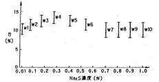
図5は、Na2S水溶液の濃度を変えて光吸収層5′を作製したときのエネルギー変換効率η〔%〕S=0.16の測定結果を示す特性図である。複数の試料を用いたときの測定範囲をw1,w2,w3,…によってあらわしている。
【0048】
この測定結果によれば、Na2S水溶液の濃度は、エネルギー変換効率ηの点からして、0.01〜1.0(5)の範囲が適正である。その場合、Na2S水溶液の濃度が薄いとエネルギー変換効率ηが悪くなり、濃いとMo電極2とSLG基板1との間でエッチングによる剥離が生じてしまう。
【0049】
図Gは、Na2S水溶液(濃度0.27%)の液温を変えて光吸収層5′を作製したときのエネルギー変換効率η〔%〕S=0.16の測定結果を示す特性図である。
【0050】
この測定結果によれば、Na2S水溶液の液温は、エネルギー変換効率ηの点からして、常温10℃〜70℃の範囲が適正である(望ましくは15℃〜40℃の範囲)。その場合、Na2S水溶液の液温が低いとエネルギー変換効率ηが悪くなり、80℃以上だとMo電極2とSLG基板1との間でエッチングによる剥離が生じてしまう。
【0051】
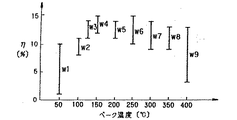
図7は、アルカリ層9をベーク処理(処理時間60分)するときのベーク温度を変えて光吸収層5′を作製したときのエネルギー変換効率η〔%〕S=0.16の測定結果を示す特性図である。
【0052】
この測定結果によれば、ベーク温度は、エネルギー変換効率ηの点からして、100℃〜400℃の範囲が適正である(望ましくは100℃〜250℃の範囲)。その場合、ベーク温度が低いとエネルギー変換効率ηが悪くなり、高いとアルカリ層9の含水率が減少して剥離しやすくなってしまう。
【0053】
図8は、アルカリ層9を温度150℃でベーク処理するときのベーク時間を変えて光吸収層5′を作製したときのエネルギー変換効率η〔%〕S=0.16の測定結果を示す特性図である。
【0054】
この測定結果によれば、ベーク時間は、エネルギー変換効率ηおよび作業性の点からして、10〜60分の範囲が適正である。
【0055】
本発明は、浸漬法によってアルカリ層9を形成するのに用いるIa族元素を含む水溶液として、Na2S・9H2O水和物を用いる以外に、その他のアルカリ金属またはその硫化物、水酸化物、塩化物等の水溶液を用いることが可能である。
【0056】
具体的には、以下の水溶液が用いられる。
Na化合物:Na2SeO3・5H2O、Na2TeO3・5H2O、Na2SO3・7H2O、Na2B4O7・10H2O、AlNa(SO4)2・12H2O、NaCl
K化合物:K2TeO3・3H2O、K2Al2O4・3H2O、AlK(SO4)2・12H2O、KOH、KF
Li
【0057】
また、本発明では、Mo電極層2′上にIn層41を設けたうえで、その上にCu−Ga合金層42を設けて積層プリカーサ4を形成するようにしているので、Mo電極層2′との界面における元素の固層拡散による合金化を抑制することができる。そして、その積層プリカーサ4をSe雰囲気中で熱処理してセレン化する際に、Mo電極層2′側にIn成分を充分に拡散させることができるとともに、拡散速度の遅いGaがMo電極層2′との界面に偏析して結晶性の悪いCu−Ga−Se層が形成されることがないようにして、均一な結晶による高品質なP型半導体のCu(In+Ga)Se2によるCIGSの光吸収層5′を作製することができる。
【0058】
したがって、Mo電極層2′と光吸収層5′との間に、結晶性が悪くて構造的に脆く、かつ導電性を有する異層(Cu−Ga−Se層)が介在するようなことがなくなり、Mo電極層2′との密着性が高くて構造的に強固な、しかも電池特性の良好な太陽電池を得ることができるようになる。
【0059】
また、図9に示すように、例えばMo電極層2′上にCu−Ga層42をIn層41、43によって挟んだ構造の積層プリカーサ4′をスパッタリングによって形成するようにしてもよい。
【0060】
この場合には、Mo電極層2′にIn層41を設けたうえで、その上にCu−Ga層42を設けるようにしているので、Mo電極層2′との界面における元素の固層拡散による合金化を抑制することができる。そして、積層プリカーサ4をSe雰囲気中で熱処理してセレン化する際に、Mo電極層2′側にIn成分を充分に拡散させることができるとともに、拡散速度の遅いGaがMo電極層2′との界面に偏析して結晶性の悪いCu−Ga−Se層が形成されることがなくなる。また、表面がIn層43によって被覆されているので、セレン化によって作製される光吸収層の表面に導電性を有する異層Cu2Seが生成されることがなくなる。
【0061】
したがって、この場合には、Mo電極層2′との密着性が高くて構造的に強固な、しかもリークのない電池特性の良好な太陽電池を得ることができるようになる。
【0062】
図10および図11は、本発明による薄膜太陽電池の製造方法の他の例を示している。
【0063】
ここでは、特に、Mo電極2″として、第1のMo電極層21と第2のMo電極層22との積層構造となるように、第1のスパッタリング工程によってSLG基板1に対する密着性を確保するために固定条件下でMo電極層21を成膜したうえで(ステップS2)、第2のスパッタリング工程によって成膜圧力を調整してアルカリ金属元素の拡散量を制御するためのMo電極層22を成膜するようにしている(ステップS3)。
【0064】
そして、熱処理時にSLG基板1とMo電極2″との熱膨張係数の差などによって生ずる熱応力によってSLG基板1とMo電極2″との間が剥離することがないように、SLG基板1とMo電極層21との間にSiO2、Al2O3などからなる応力緩和層8をCVD法によって成膜するようにしている。
【0065】
スパッタリングによる第1のMo電極層21の固定の成膜条件としては、以下のとおりである。
圧力:4Pa、供給電力:3KW、Arガス流量:100sccm、膜厚:500Å
【0066】
スパッタリングによる第2のMo電極層22の成膜条件としては、以下のとおりである。
圧力:0.7〜6Pa、供給電力:9KW、Arガス流量:100sccm、膜厚:3500Å
【0067】
表1は、スパッタリングによって第2のMo電極層22を上記の条件下で圧力を0.7〜6Paの範囲でそれぞれ変化させて成膜させることによって製造した各太陽電池の光電変換効率η、極性因子FFおよび開放電圧Vocを測定した結果を示している。
【0068】
【表1】

表1では、アルカリ層9を設けない構造にあって、第2のMo電極層22の成膜時の圧力が2Paのときの各測定結果を基準値1として、圧力が0.7Pa、3〜6Paのときの各測定値をその基準値で規格化している。
【0070】
この測定結果によれば、圧力を3〜6Paにしたときの光電変換効率η、極性因子FFおよび開放電圧Vocの各測定値が電池特性として最良の値を示している。したがって、この場合には、圧力:3〜6Pa、供給電力:9KW、Arガス流量:100sccm、膜厚:3500Åの最適条件下で第2のMo電極層22を成膜するようにすれば、SLG基板1から光吸収層5′へのNa元素の拡散量を適正に制御することができるようになる。
【0071】
【効果】
以上、本発明によれば、基板上に裏面電極層を形成し、その裏面電極層上にプリカーサ膜を形成して、SeまたはS雰囲気中で熱処理することによってCIGS系の光吸収層を作製し、その光吸収層上にバッファ層を介して透明電極層を形成するに際して、前記基板にアルカリ成分を含む基板を用いるとともに、Ia族元素を含む水溶液に裏面電極層を浸漬したのち乾燥させて裏面電極層上にアルカリ層を形成するようにして、前記熱処理時にその基板およびアルカリ層からそれぞれアルカリ金属元素が光吸収層に拡散するようにしたうえで、前記裏面電極をPVD法にて成膜することにより前記基板からのアルカリ金属元素が光吸収層に拡散する拡散量をPVD法の成膜圧力の変化により膜質を変化させて、前記アルカリ層と前記基板からのアルカリ金属元素が単位面積あたり10E+10〜10E+16の範囲原子数密度をもって光吸収層に拡散されるようにしているので、効率良く適正に光吸収層にアルカリ金属元素を拡散させることができるようになり、エネルギー変換効率の良い太陽電池を容易に得ることができるという利点を有している。
【0072】
そして、本発明によれば、その裏面電極層として、固定条件によって一律に形成した第1の裏面電極層と、アルカリ金属元素の拡散量を制御できるように膜質や膜厚を調整した第2の裏面電極層との積層構造としているので、第1の裏面電極層によって基板に対する密着性を確保しながら、第2の裏面電極層によって光吸収層にアルカリ金属元素の拡散を適正に行わせることができるようになる。
【0073】
また、本発明によれば、Ia族元素を含む水溶液に裏面電極層を浸漬したのち乾燥させて裏面電極層上にアルカリ層を形成するようにしているので、変質や剥離の問題を生ずることなく、簡単な工程によって膜質の安定したアルカリ層を得ることができるようになる。
【0074】
また、本発明によれば、基板と裏面電極層との間に応力緩和層を設けるようにしているので、熱処理時に生ずる熱応力によって基板と裏面電極層との間が剥離するようなことを有効に防止して、構造的に強固な太陽電池を製造することができるという利点を有している。
【図面の簡単な説明】
【図1】一般的な化合物半導体による薄膜太陽電池の基本的な構造を示す正断面図である。
【図2】従来の裏面電極上に光吸収層を作製するプロセスを示す図である。
【図3】本発明の基本的な薄膜太陽電池の構造方法によって、基板上に裏面電極、アルカリ層、積層プリカーサを形成するまでのプロセスを示す図である。
【図4】本発明の基本的な薄膜太陽電池の構造方法によって、積層プリカーサを熱処理して光吸収層を得て、その上にバッファ層を介して透明電極層を形成するまでのプロセスを示す図である。
【図5】Na2S水溶液の濃度を変えて光吸収層を作製したときのエネルギー変換効率の測定結果を示す特性図である。
【図6】Na2S水溶液の液温を変えて光吸収層を作製したときのエネルギー変換効率の測定結果を示す特性図である。
【図7】アルカリ層をベーク処理するときの温度を変えて光吸収層を作製したときのエネルギー変換効率の測定結果を示す特性図である。
【図8】アルカリ層をベーク処理するときの時間を変えて光吸収層を作製したときのエネルギー変換効率の測定結果を示す特性図である。
【図9】アルカリ層上にCu−Ga合金層をIn層で挟んだ構造の積層プリカーサを示す正断面図である。
【図10】本発明による薄膜太陽電池の構造方法によって、基板上に応力緩和層、裏面電極層、アルカリ層を形成するまでのプロセスを示す図である。
【図11】本発明による薄膜太陽電池の構造方法によって、アルカリ層上に積層プリカーサを形成し、そのプリカーサを熱処理して光吸収層を得て、その上にバッファ層を介して透明電極層を形成するまでのプロセスを示す図である。
【符号の説明】
1 SLG基板
2′ Mo電極層(裏面電極)
2″ Mo電極層(裏面電極)
21 第1のMo電極層(第1の裏面電極層)
22 第2のMo電極層(第1の裏面電極層)
4 積層プリカーサ
5′ 光吸収層
6 バッファ層
7 透明電極層
8 応力緩和層
9 アルカリ層[0001]
[Industrial application fields]
The present invention relates to a method for manufacturing a thin film solar cell using a compound semiconductor.
[0002]
[Prior art]
FIG. 1 shows a basic structure of a thin film solar cell made of a general chalcopyrite compound semiconductor. That is, a
[0003]
As the
[0004]
Conventionally, as a method of producing a light absorption layer using a CIGS thin film, there is a selenization method in which a Se compound is generated by a thermochemical reaction using a Se source such as
[0005]
In US Pat. No. 4,798,660, a metal thin film layer formed by DC magnetron sputtering and having a structure in which a back electrode layer, a pure Cu single layer, and a pure In single layer are stacked in this order is formed in an Se atmosphere, preferably in H2Se gas. It is disclosed to form a light absorption layer composed of a CIS single phase having a uniform composition by selenization.
[0006]
In JP-A-10-135495, as a metal precursor, a metal thin film formed by sputtering using a Cu—Ga alloy target and a metal thin film formed by sputtering using an In target are used. Things are shown.
[0007]
As shown in FIG. 2, when forming the
[0008]
However, when the
[0009]
For this reason, it has been proposed to provide a Ga concentration gradient so that the Ga concentration decreases from the interface with the
[0010]
However, according to such a conventional method for forming a light absorption layer, since Ga segregates at the interface between the
[0011]
Conventionally, it has been shown that the alkali metal element (Na element) in the soda lime glass serving as the substrate diffuses into the CuInSe2 film to grow grains, and the solar cell using the CuInSe2 film in which the alkali metal element has diffused is shown. It has been reported that the energy conversion efficiency is increased ("THE INFLUENCE OF SODIUM ON THE GRAIN STRUCTURE OF OF CuInSe2 FILMS FOR PHOTOVOLTAIC APPLICATIONS") by the 12th European Photovoltaic Solar Energy Conference M. Bodegard et al.
[0012]
Furthermore, the resistance value of the CIGS film deposited on the glass containing the alkali component is small, and in the solar cell in which the CIGS film is formed after depositing the Na2O2 film on the substrate, the energy conversion efficiency does not deposit the Na2O2 film. It has been reported that the energy conversion efficiency, which is about 2% higher than that of solar cells, and which is usually highly dependent on the Cu / In ratio, is constant regardless of the Cu / In ratio. {1st Photovoltaic Energy Conversion World Conference M.M. "INFRUENCE OF SUBSTRATES ON THE ELECTRICAL PROPERITES OF Cu (In, Gs) Se2 THINFILMS"} by Ruckh et al.}.
[0013]
As can be seen from the above reports, diffusion or addition of alkali metal elements is effective for promoting the growth of the CuInSe2 film, increasing the carrier concentration, and improving the energy conversion efficiency of the solar cell.
[0014]
As a method for doping an alkali metal element, there is a method in which an alkali layer containing an alkali metal element is formed on a Mo electrode (back electrode) layer by vapor deposition or sputtering, and then a laminated precursor is formed and selenized. It is shown in the specification of No. 8-222750. The problem of this manufacturing method is that the alkali layer made of Na or Na compound has a hygroscopic property, so that it changes in quality when it is exposed to the air after film formation, resulting in peeling.
[0015]
For this reason, US Pat. No. 542204 discloses a method for producing a CuInSe2 film by a vapor deposition method in which an alkali metal element is doped simultaneously with other elements constituting the light absorption layer. Also disclosed is a method of depositing Cu—In—O: Na 2
[0016]
JP-A-8-222750 discloses that a barrier layer is provided between the SLG substrate and the light absorption layer in order to prevent diffusion of alkali metal elements from the SLG substrate to the light absorption layer, or The use of a substrate that does not contain an alkali metal is disclosed.
[0017]
[Problems to be solved by the invention]
The problem to be solved is that a CIGS-based light is formed by forming a laminated precursor film composed of a Cu—Ga alloy layer and an In layer on a back electrode layer in a thin film solar cell using a compound semiconductor, and performing heat treatment in an Se atmosphere. In forming the absorption layer, in order to diffuse the alkali metal element in the light absorption layer in order to improve the energy conversion efficiency, the alkali layer is formed on the back electrode layer by vapor deposition or sputtering, so that the film is formed. That is, the alkali layer is denatured and easily peeled off.
[0018]
In addition, an alkali metal element is doped during selenization of the laminated precursor, or Cu—In—O: Na 2
[0019]
Further, a barrier layer for preventing diffusion of an alkali metal element from the SLG substrate to the light absorption layer is provided between the SLG substrate and the light absorption layer, or a back electrode is formed using a substrate that does not contain an alkali metal element. If the alkali metal element is diffused from the alkali layer provided on the layer to the light absorption layer, there is a problem that the efficiency is poor.
[0020]
[Means for Solving the Problems]
The present invention forms a CIGS-based light absorption layer by forming a back electrode layer on a substrate, forming a precursor film on the back electrode layer, and heat-treating it in a Se or S atmosphere. A method for manufacturing a thin-film solar cell in which a transparent electrode layer is formed on an absorption layer through a buffer layer so that an alkali metal element can be efficiently and effectively diffused into the light absorption layer during the heat treatment. In order to The substrate And using a substrate containing an alkaline component, A back electrode layer is immersed in an aqueous solution containing a group Ia element and then dried to form an alkali layer on the back electrode layer. The alkali metal element diffuses from the substrate and the alkali layer to the light absorption layer at the time of the heat treatment, and the alkali metal element from the substrate absorbs the light by forming the back electrode by a PVD method. By changing the film quality by changing the film formation pressure of the PVD method, The alkali metal element from the alkali layer and the substrate is diffused into the light absorption layer with an atomic number density in the range of 10E + 10 to 10E + 16 per unit area. I am doing so.
[0021]
Specifically, the diffusion amount of the alkali metal element is controlled by optimizing the film thickness and film quality of the back electrode.
[0022]
According to the present invention, a fixed first back electrode layer for securing adhesion to the substrate and a second back surface for controlling the diffusion amount of the alkali metal element on the substrate containing an alkali component. A back electrode having a laminated structure with the electrode layer is formed.
[0023]
Further, in the present invention, when a precursor film is formed on a back electrode in a thin film solar cell using a compound semiconductor and heat treatment is performed in an Se atmosphere, a CIGS-based light absorption layer is produced to improve energy conversion efficiency. After immersing the back electrode in an aqueous solution containing a group Ia element, a layer for diffusing an alkali metal element in the light absorption layer can be obtained by a simple process without causing deterioration or peeling. An alkali layer is formed on the back electrode by drying.
[0024]
Furthermore, according to the present invention, a stress relaxation layer is provided between the substrate and the back electrode so that the substrate and the back electrode are not separated by thermal stress generated during the heat treatment.
[0025]
【Example】
In the method of manufacturing a thin-film solar cell according to the present invention, basically, as shown in FIG. 3, the diffusion amount of alkali metal element (Na) contained in the
[0026]
Next, an
[0027]
As the film formation of the
[0028]
Next, after the In
[0029]
Then, as shown in FIG. 4, the
[0030]
During this heat treatment, an amount of alkali metal element optimally controlled by the
[0031]
At that time, the
[0032]
Further, the film quality and film thickness of the Mo electrode layer 2 'are set so that the alkali metal element diffusing from the
[0033]
It is known that various characteristics as a thin film are changed by changing the film forming conditions (temperature, pressure, supply power, etc.) of the thin film by sputtering. In the present invention, the amount of alkali metal element diffused from the
[0034]
Specifically, unit area 1cm 2 The alkali metal element is diffused into the
[0035]
Next, a
[0036]
As described above, according to the present invention, when the
[0037]
The
[0038]
That is, the
[0039]
Also, if an aqueous solution of Na2S · 9H2O is used, the surface oxide film of the Mo electrode layer 2 'is effectively adjusted by adjusting its concentration to a range of 11 to 13 pH where the surface oxide film of the Mo electrode layer 2' can be etched. In addition, since the S component is contained, the adhesion between the
[0040]
Advantages of forming the
[0041]
A large-scale apparatus such as sputtering or vacuum deposition is not required, and it can be realized with a relatively simple apparatus. In addition, when a vacuum apparatus is used, quality control of a sputtering target, a vacuum evaporation source, or the like is difficult, but a material such as Na2S has high hygroscopicity, so that the humidity of the material can be easily managed by the dipping method.
[0042]
Even on a substrate or electrode surface having a texture structure for confining light, it is possible to form an
[0043]
When immersing the surface of the Mo electrode layer 2 ', an etching effect and a particle removal effect of the surface oxide film of the Mo electrode layer 2' can be obtained by using an alkali metal aqueous solution. Thereby, it becomes possible to omit the surface cleaning process after laser scribing of the Mo electrode layer 2 '. Moreover, in order to perform the surface cleaning of the Mo electrode layer 2 'more effectively, the pH can be easily adjusted by adding ammonia, NaOH or the like to the solution.
[0044]
Due to the immersion of the aqueous solution, oxygen and hydrogen remain in the
[0045]
The findings of the amount of alkali metal deposited when the
[0046]
Using two samples diluted with 1Y16-51 Na2S 0.2% and 1Y16-52 Na2S 0.8%, respectively, 6 ml of ultrapure water was dropped on the film-forming portion by ICP-MS analysis. Na was collected while scanning with a transfer tool for 5 minutes. As a result, in the former sample, 2.8E + 15 (atoms / cm per unit area) 2 ), And in the latter sample, 8,7E + 15 (atoms / cm per unit area) 2 ) Number of atoms was obtained. The limit of quantification is about 2E + 10.
[0047]
FIG. 5 is a characteristic diagram showing a measurement result of energy conversion efficiency η [%] S = 0.16 when the
[0048]
According to this measurement result, the concentration of the Na 2 S aqueous solution is appropriately in the range of 0.01 to 1.0 (5) in terms of energy conversion efficiency η. In that case, if the concentration of the Na 2 S aqueous solution is low, the energy conversion efficiency η is deteriorated, and if it is high, peeling by etching occurs between the
[0049]
FIG. G is a characteristic diagram showing the measurement result of energy conversion efficiency η [%] S = 0.16 when the
[0050]
According to this measurement result, the liquid temperature of the Na 2 S aqueous solution is appropriately in the range of 10 ° C. to 70 ° C. at room temperature (preferably in the range of 15 ° C. to 40 ° C.) in terms of energy conversion efficiency η. In that case, if the liquid temperature of the Na 2 S aqueous solution is low, the energy conversion efficiency η is deteriorated, and if it is 80 ° C. or higher, peeling by etching occurs between the
[0051]
FIG. 7 shows the measurement result of energy conversion efficiency η [%] S = 0.16 when the
[0052]
According to this measurement result, the baking temperature is suitably in the range of 100 ° C. to 400 ° C. (preferably in the range of 100 ° C. to 250 ° C.) in terms of energy conversion efficiency η. In that case, when the baking temperature is low, the energy conversion efficiency η is deteriorated, and when the baking temperature is high, the moisture content of the
[0053]
FIG. 8 is a characteristic showing measurement results of energy conversion efficiency η [%] S = 0.16 when the
[0054]
According to this measurement result, the baking time is appropriately in the range of 10 to 60 minutes from the viewpoint of energy conversion efficiency η and workability.
[0055]
The present invention is not limited to using Na2S.9H2O hydrate as an aqueous solution containing a group Ia element used for forming the
[0056]
Specifically, the following aqueous solutions are used.
Na compound: Na2SeO3 · 5H2O, Na2TeO3 · 5H2O, Na2SO3 · 7H2O, Na2B4O7 · 10H2O, AlNa (SO4) 2 · 12H2O, NaCl
K compound: K2TeO3 · 3H2O, K2Al2O4 · 3H2O, AlK (SO4) 2 · 12H2O, KOH, KF
Li
[0057]
In the present invention, since the
[0058]
Therefore, a different layer (Cu—Ga—Se layer) having poor crystallinity and structurally brittle and conductive is interposed between the
[0059]
As shown in FIG. 9, for example, a laminated precursor 4 'having a structure in which a Cu-
[0060]
In this case, since the
[0061]
Therefore, in this case, it is possible to obtain a solar cell that has high adhesion to the Mo electrode layer 2 ', is structurally strong, and has good battery characteristics without leakage.
[0062]
10 and 11 show another example of a method for manufacturing a thin-film solar cell according to the present invention.
[0063]
Here, in particular, the adhesion to the
[0064]
Then, the
[0065]
The film forming conditions for fixing the first
Pressure: 4 Pa, Supply power: 3 KW, Ar gas flow rate: 100 sccm, Film thickness: 500 mm
[0066]
The conditions for forming the second
Pressure: 0.7-6 Pa, Supply power: 9 kW, Ar gas flow rate: 100 sccm, Film thickness: 3500 mm
[0067]
Table 1 shows the photoelectric conversion efficiency η and polarity of each solar cell manufactured by sputtering to form the second
[0068]
[Table 1]
In Table 1, in the structure in which the
[0070]
According to this measurement result, the measured values of photoelectric conversion efficiency η, polarity factor FF, and open circuit voltage Voc when the pressure is set to 3 to 6 Pa show the best values as battery characteristics. Therefore, in this case, if the second
[0071]
【effect】
As described above, according to the present invention, a CIGS-based light absorption layer is formed by forming a back electrode layer on a substrate, forming a precursor film on the back electrode layer, and performing heat treatment in a Se or S atmosphere. In forming a transparent electrode layer on the light absorption layer via a buffer layer, The substrate And using a substrate containing an alkaline component, A back electrode layer is immersed in an aqueous solution containing a group Ia element and then dried to form an alkali layer on the back electrode layer. The alkali metal element diffuses from the substrate and the alkali layer to the light absorption layer at the time of the heat treatment, and the alkali metal element from the substrate absorbs the light by forming the back electrode by a PVD method. By changing the film quality by changing the film formation pressure of the PVD method, The alkali metal element from the alkali layer and the substrate is diffused into the light absorption layer with an atomic number density in the range of 10E + 10 to 10E + 16 per unit area. Thus, the alkali metal element can be diffused efficiently and appropriately in the light absorption layer, and there is an advantage that a solar cell with high energy conversion efficiency can be easily obtained.
[0072]
And according to this invention, as the back electrode layer, the 1st back electrode layer formed uniformly by fixed conditions, and the 2nd which adjusted film quality and film thickness so that the diffusion amount of an alkali metal element could be controlled Since it has a laminated structure with the back electrode layer, it is possible to appropriately diffuse the alkali metal element in the light absorption layer with the second back electrode layer while ensuring adhesion to the substrate with the first back electrode layer. become able to.
[0073]
Further, according to the present invention, the back electrode layer is immersed in an aqueous solution containing a group Ia element and then dried to form an alkali layer on the back electrode layer. An alkaline layer having a stable film quality can be obtained by a simple process.
[0074]
In addition, according to the present invention, since the stress relaxation layer is provided between the substrate and the back electrode layer, it is effective that the substrate and the back electrode layer are separated due to the thermal stress generated during the heat treatment. This has the advantage that a structurally strong solar cell can be produced.
[Brief description of the drawings]
FIG. 1 is a front sectional view showing a basic structure of a thin film solar cell using a general compound semiconductor.
FIG. 2 is a diagram showing a process for producing a light absorption layer on a conventional back electrode.
FIG. 3 is a diagram showing a process up to formation of a back electrode, an alkali layer, and a laminated precursor on a substrate by the basic thin-film solar cell structure method of the present invention.
FIG. 4 shows a process from a heat treatment of a laminated precursor to obtain a light absorption layer by the basic thin film solar cell structure method of the present invention, and a formation of a transparent electrode layer thereon via a buffer layer. FIG.
FIG. 5 is a characteristic diagram showing measurement results of energy conversion efficiency when a light absorption layer is produced by changing the concentration of an aqueous Na 2 S solution.
FIG. 6 is a characteristic diagram showing measurement results of energy conversion efficiency when a light absorption layer is produced by changing the liquid temperature of an Na 2 S aqueous solution.
FIG. 7 is a characteristic diagram showing measurement results of energy conversion efficiency when a light absorption layer is produced by changing the temperature at the time of baking an alkali layer.
FIG. 8 is a characteristic diagram showing measurement results of energy conversion efficiency when a light absorption layer is produced by changing the time when baking an alkali layer.
FIG. 9 is a front sectional view showing a laminated precursor having a structure in which a Cu—Ga alloy layer is sandwiched between In layers on an alkali layer.
FIG. 10 is a diagram showing a process until a stress relaxation layer, a back electrode layer, and an alkali layer are formed on a substrate by the thin-film solar cell structure method according to the present invention.
FIG. 11 shows a thin film solar cell structure method according to the present invention, in which a laminated precursor is formed on an alkali layer, the precursor is heat-treated to obtain a light absorption layer, and a transparent electrode layer is formed thereon via a buffer layer. It is a figure which shows the process until it forms.
[Explanation of symbols]
1 SLG substrate
2 'Mo electrode layer (back electrode)
2 ″ Mo electrode layer (back electrode)
21 1st Mo electrode layer (1st back surface electrode layer)
22 Second Mo electrode layer (first back electrode layer)
4 Laminated precursor
5 'light absorption layer
6 Buffer layer
7 Transparent electrode layer
8 Stress relaxation layer
9 Alkaline layer
Claims (5)
Priority Applications (1)
| Application Number | Priority Date | Filing Date | Title |
|---|---|---|---|
| JP2002337272A JP4055064B2 (en) | 2002-10-16 | 2002-10-16 | Method for manufacturing thin film solar cell |
Applications Claiming Priority (1)
| Application Number | Priority Date | Filing Date | Title |
|---|---|---|---|
| JP2002337272A JP4055064B2 (en) | 2002-10-16 | 2002-10-16 | Method for manufacturing thin film solar cell |
Publications (3)
| Publication Number | Publication Date |
|---|---|
| JP2004140307A JP2004140307A (en) | 2004-05-13 |
| JP2004140307A5 JP2004140307A5 (en) | 2005-06-30 |
| JP4055064B2 true JP4055064B2 (en) | 2008-03-05 |
Family
ID=32462622
Family Applications (1)
| Application Number | Title | Priority Date | Filing Date |
|---|---|---|---|
| JP2002337272A Expired - Fee Related JP4055064B2 (en) | 2002-10-16 | 2002-10-16 | Method for manufacturing thin film solar cell |
Country Status (1)
| Country | Link |
|---|---|
| JP (1) | JP4055064B2 (en) |
Families Citing this family (12)
| Publication number | Priority date | Publication date | Assignee | Title |
|---|---|---|---|---|
| US20080128085A1 (en) * | 2004-12-01 | 2008-06-05 | Mimasu Semiconductor Industry Co., Ltd. | Surface Treating Apparatus For Square Wafer For Solar Battery |
| JP2006165386A (en) * | 2004-12-09 | 2006-06-22 | Showa Shell Sekiyu Kk | Cis system thin film solar cell and method for manufacturing the same |
| JP4969785B2 (en) * | 2005-02-16 | 2012-07-04 | 本田技研工業株式会社 | Chalcopyrite solar cell and method for manufacturing the same |
| JP2007201304A (en) * | 2006-01-30 | 2007-08-09 | Honda Motor Co Ltd | Solar cell and its manufacturing method |
| JP4794480B2 (en) * | 2007-03-05 | 2011-10-19 | 本田技研工業株式会社 | Ia group element measurement method |
| FR2924863B1 (en) † | 2007-12-07 | 2017-06-16 | Saint Gobain | IMPROVEMENTS TO ELEMENTS CAPABLE OF COLLECTING LIGHT. |
| JP4384237B2 (en) * | 2008-05-19 | 2009-12-16 | 昭和シェル石油株式会社 | CIS type thin film solar cell manufacturing method |
| JP4540724B2 (en) * | 2008-05-20 | 2010-09-08 | 昭和シェル石油株式会社 | CIS type thin film solar cell manufacturing method |
| JP4782855B2 (en) * | 2009-03-12 | 2011-09-28 | 昭和シェル石油株式会社 | Compound-based thin-film solar cell and method for producing the same |
| KR101373787B1 (en) * | 2011-01-12 | 2014-03-17 | 지에스칼텍스 주식회사 | Method of manufacturing thin film solar cell using alkali hydride |
| JP5174230B1 (en) | 2011-11-25 | 2013-04-03 | 昭和シェル石油株式会社 | Thin film solar cell module and manufacturing method thereof |
| CN110854239A (en) * | 2019-11-26 | 2020-02-28 | 龙焱能源科技(杭州)有限公司 | Thin film solar cell and manufacturing method thereof |
-
2002
- 2002-10-16 JP JP2002337272A patent/JP4055064B2/en not_active Expired - Fee Related
Also Published As
| Publication number | Publication date |
|---|---|
| JP2004140307A (en) | 2004-05-13 |
Similar Documents
| Publication | Publication Date | Title |
|---|---|---|
| JP3876440B2 (en) | Method for producing light absorption layer | |
| JP4110515B2 (en) | Thin film solar cell and manufacturing method thereof | |
| JP4680183B2 (en) | Method for producing chalcopyrite thin film solar cell | |
| US8425739B1 (en) | In chamber sodium doping process and system for large scale cigs based thin film photovoltaic materials | |
| US8691619B2 (en) | Laminated structure for CIS based solar cell, and integrated structure and manufacturing method for CIS based thin-film solar cell | |
| JP6096790B2 (en) | Conductive substrate for photovoltaic cells | |
| US20120018828A1 (en) | Sodium Sputtering Doping Method for Large Scale CIGS Based Thin Film Photovoltaic Materials | |
| KR20090106513A (en) | Doping techniques for group ?????? compound layers | |
| US20060219288A1 (en) | Process and photovoltaic device using an akali-containing layer | |
| Basol et al. | Deposition of CuInSe/sub 2/films by a two-stage process utilizing E-beam evaporation | |
| US20100297835A1 (en) | Methods for fabricating copper indium gallium diselenide (cigs) compound thin films | |
| WO2009045565A1 (en) | Roll to roll evaporation tool for solar absorber precursor formation | |
| JP4055064B2 (en) | Method for manufacturing thin film solar cell | |
| JP2004015039A (en) | Compound thin film solar cell and method for manufacturing the same | |
| JP3311873B2 (en) | Manufacturing method of semiconductor thin film | |
| JP2004047917A (en) | Thin film solar battery and its manufacturing method | |
| US20140048132A1 (en) | Solar cell and method of preparing the same | |
| Basol et al. | CuInSe2 films and solar cells obtained by selenization of evaporated Cu‐In layers | |
| JP2017128792A (en) | Method for forming acigs thin film at low-temperature and method for manufacturing solar cell using the same | |
| KR20140047760A (en) | Manufacturing method of solar cell light absortion layer | |
| JP2003258282A (en) | Method for forming optical absorption layer | |
| KR20180034248A (en) | Flexible CZTS-based thin film solar cell using sodium hydroxide and manufacturing method thereof | |
| CN111223963B (en) | Alkali metal doping treatment method for large-scale production of copper indium gallium selenide thin-film solar cells | |
| CN107735867B (en) | Photovoltaic cell and manufacturing method thereof | |
| WO2013141644A1 (en) | Method for manufacturing chalcogenide solar cell having dual texture structure in which texture is formed on surface of rear surface electrode, and chalcogenide solar cell manufactured thereby |
Legal Events
| Date | Code | Title | Description |
|---|---|---|---|
| A521 | Request for written amendment filed |
Free format text: JAPANESE INTERMEDIATE CODE: A523 Effective date: 20041008 |
|
| A621 | Written request for application examination |
Free format text: JAPANESE INTERMEDIATE CODE: A621 Effective date: 20041008 |
|
| A977 | Report on retrieval |
Free format text: JAPANESE INTERMEDIATE CODE: A971007 Effective date: 20070627 |
|
| A131 | Notification of reasons for refusal |
Free format text: JAPANESE INTERMEDIATE CODE: A131 Effective date: 20070710 |
|
| A521 | Request for written amendment filed |
Free format text: JAPANESE INTERMEDIATE CODE: A523 Effective date: 20070907 |
|
| TRDD | Decision of grant or rejection written | ||
| A01 | Written decision to grant a patent or to grant a registration (utility model) |
Free format text: JAPANESE INTERMEDIATE CODE: A01 Effective date: 20071120 |
|
| A61 | First payment of annual fees (during grant procedure) |
Free format text: JAPANESE INTERMEDIATE CODE: A61 Effective date: 20071128 |
|
| R150 | Certificate of patent or registration of utility model |
Free format text: JAPANESE INTERMEDIATE CODE: R150 |
|
| FPAY | Renewal fee payment (event date is renewal date of database) |
Free format text: PAYMENT UNTIL: 20101221 Year of fee payment: 3 |
|
| FPAY | Renewal fee payment (event date is renewal date of database) |
Free format text: PAYMENT UNTIL: 20101221 Year of fee payment: 3 |
|
| FPAY | Renewal fee payment (event date is renewal date of database) |
Free format text: PAYMENT UNTIL: 20111221 Year of fee payment: 4 |
|
| FPAY | Renewal fee payment (event date is renewal date of database) |
Free format text: PAYMENT UNTIL: 20111221 Year of fee payment: 4 |
|
| FPAY | Renewal fee payment (event date is renewal date of database) |
Free format text: PAYMENT UNTIL: 20121221 Year of fee payment: 5 |
|
| FPAY | Renewal fee payment (event date is renewal date of database) |
Free format text: PAYMENT UNTIL: 20131221 Year of fee payment: 6 |
|
| LAPS | Cancellation because of no payment of annual fees |