EP1474748B1 - Techniques for facilitating conversion between asynchronous and synchronous domains - Google Patents
Techniques for facilitating conversion between asynchronous and synchronous domains Download PDFInfo
- Publication number
- EP1474748B1 EP1474748B1 EP03711026A EP03711026A EP1474748B1 EP 1474748 B1 EP1474748 B1 EP 1474748B1 EP 03711026 A EP03711026 A EP 03711026A EP 03711026 A EP03711026 A EP 03711026A EP 1474748 B1 EP1474748 B1 EP 1474748B1
- Authority
- EP
- European Patent Office
- Prior art keywords
- data
- transfer
- asynchronous
- synchronous
- token
- Prior art date
- Legal status (The legal status is an assumption and is not a legal conclusion. Google has not performed a legal analysis and makes no representation as to the accuracy of the status listed.)
- Expired - Lifetime
Links
- 230000001360 synchronised effect Effects 0.000 title claims abstract description 230
- 238000000034 method Methods 0.000 title description 74
- 238000006243 chemical reaction Methods 0.000 title description 10
- 238000012546 transfer Methods 0.000 claims abstract description 220
- 230000007704 transition Effects 0.000 claims abstract description 78
- 230000004044 response Effects 0.000 claims abstract description 38
- 230000005540 biological transmission Effects 0.000 claims abstract description 21
- 239000000872 buffer Substances 0.000 claims description 148
- 230000008569 process Effects 0.000 description 64
- 238000013461 design Methods 0.000 description 49
- 230000000630 rising effect Effects 0.000 description 49
- 230000003139 buffering effect Effects 0.000 description 17
- 238000010586 diagram Methods 0.000 description 16
- 238000012163 sequencing technique Methods 0.000 description 11
- 230000007935 neutral effect Effects 0.000 description 8
- 101150110532 CFDP1 gene Proteins 0.000 description 7
- 230000000694 effects Effects 0.000 description 7
- 230000014509 gene expression Effects 0.000 description 7
- 101100284369 Neurospora crassa (strain ATCC 24698 / 74-OR23-1A / CBS 708.71 / DSM 1257 / FGSC 987) has-1 gene Proteins 0.000 description 6
- 241000761456 Nops Species 0.000 description 5
- 230000006399 behavior Effects 0.000 description 5
- 230000008901 benefit Effects 0.000 description 5
- 230000015572 biosynthetic process Effects 0.000 description 5
- 108010020615 nociceptin receptor Proteins 0.000 description 5
- 238000003786 synthesis reaction Methods 0.000 description 5
- 238000007792 addition Methods 0.000 description 4
- 238000009826 distribution Methods 0.000 description 4
- 230000006870 function Effects 0.000 description 4
- 230000007246 mechanism Effects 0.000 description 4
- 238000012545 processing Methods 0.000 description 4
- 239000004065 semiconductor Substances 0.000 description 4
- 238000013459 approach Methods 0.000 description 3
- 238000004891 communication Methods 0.000 description 3
- 230000003750 conditioning effect Effects 0.000 description 3
- 230000008520 organization Effects 0.000 description 3
- 239000000523 sample Substances 0.000 description 3
- 238000005070 sampling Methods 0.000 description 3
- 230000003068 static effect Effects 0.000 description 3
- 230000001960 triggered effect Effects 0.000 description 3
- 101100028900 Caenorhabditis elegans pcs-1 gene Proteins 0.000 description 2
- 230000001143 conditioned effect Effects 0.000 description 2
- 239000004020 conductor Substances 0.000 description 2
- 230000001351 cycling effect Effects 0.000 description 2
- 230000007717 exclusion Effects 0.000 description 2
- 238000004519 manufacturing process Methods 0.000 description 2
- 238000012986 modification Methods 0.000 description 2
- 230000004048 modification Effects 0.000 description 2
- 230000001902 propagating effect Effects 0.000 description 2
- 241000408659 Darpa Species 0.000 description 1
- 229910001218 Gallium arsenide Inorganic materials 0.000 description 1
- 101150003196 PCS1 gene Proteins 0.000 description 1
- 101100493726 Phalaenopsis sp. BIBSY212 gene Proteins 0.000 description 1
- 101100030895 Saccharomyces cerevisiae (strain ATCC 204508 / S288c) RPT4 gene Proteins 0.000 description 1
- 229910000577 Silicon-germanium Inorganic materials 0.000 description 1
- 208000003028 Stuttering Diseases 0.000 description 1
- 230000004913 activation Effects 0.000 description 1
- 238000004364 calculation method Methods 0.000 description 1
- 230000008859 change Effects 0.000 description 1
- 230000000295 complement effect Effects 0.000 description 1
- 238000000354 decomposition reaction Methods 0.000 description 1
- 230000001934 delay Effects 0.000 description 1
- 230000003111 delayed effect Effects 0.000 description 1
- 230000001419 dependent effect Effects 0.000 description 1
- 230000000368 destabilizing effect Effects 0.000 description 1
- 238000001514 detection method Methods 0.000 description 1
- 230000009977 dual effect Effects 0.000 description 1
- 239000012634 fragment Substances 0.000 description 1
- 238000005457 optimization Methods 0.000 description 1
- 230000001575 pathological effect Effects 0.000 description 1
- 230000002085 persistent effect Effects 0.000 description 1
- 230000000063 preceeding effect Effects 0.000 description 1
- 238000011112 process operation Methods 0.000 description 1
- 238000013404 process transfer Methods 0.000 description 1
- 230000000644 propagated effect Effects 0.000 description 1
- YJQZYXCXBBCEAQ-UHFFFAOYSA-N ractopamine Chemical compound C=1C=C(O)C=CC=1C(O)CNC(C)CCC1=CC=C(O)C=C1 YJQZYXCXBBCEAQ-UHFFFAOYSA-N 0.000 description 1
- 230000002441 reversible effect Effects 0.000 description 1
- 230000011218 segmentation Effects 0.000 description 1
- 230000011664 signaling Effects 0.000 description 1
- 238000004088 simulation Methods 0.000 description 1
- 235000013599 spices Nutrition 0.000 description 1
- 238000003860 storage Methods 0.000 description 1
- 230000002459 sustained effect Effects 0.000 description 1
- 230000009466 transformation Effects 0.000 description 1
- 238000013519 translation Methods 0.000 description 1
Images


Classifications
-
- G—PHYSICS
- G06—COMPUTING; CALCULATING OR COUNTING
- G06F—ELECTRIC DIGITAL DATA PROCESSING
- G06F13/00—Interconnection of, or transfer of information or other signals between, memories, input/output devices or central processing units
- G06F13/38—Information transfer, e.g. on bus
- G06F13/40—Bus structure
- G06F13/4004—Coupling between buses
- G06F13/4027—Coupling between buses using bus bridges
- G06F13/405—Coupling between buses using bus bridges where the bridge performs a synchronising function
- G06F13/4059—Coupling between buses using bus bridges where the bridge performs a synchronising function where the synchronisation uses buffers, e.g. for speed matching between buses
Definitions
- the present invention relates to systems integrating asynchronous and synchronous components. More specifically, the invention provides methods and apparatus for facilitating conversion of data between asynchronous and synchronous domains.
- Asynchronous design methodologies and the resulting circuits and systems are emerging as a likely mechanism by which the performance of digital systems can continue the historical adherence to Moore's Law which postulates a monotonic increase in available data processing power over time.
- Moore's Law which postulates a monotonic increase in available data processing power over time.
- As asynchronous circuits and systems become more commonplace there will be an increasing need to integrate such circuits and systems with circuits and systems designed according to currently prevalent synchronous design methodologies. More specifically, there will be a need to provide low-penalty interfaces for converting data between the asynchronous and synchronous domains.
- the latency associated with conversion of a single bit of data encoded using 1 of 2 encoding may be 2 or more clock cycles due to the fact that the validity of the data to be transferred must be verified. While tolerating such latency may be feasible where the asynchronous signal is only generated infrequently or is only one bit, allowing sufficient time for eliminating metastability and verifying validity when 32 or 64 bits of data are involved is not.
- synchronous systems e.g., memory architectures such as SDRAM systems
- memory architectures such as SDRAM systems
- SDRAM systems are not tolerant of "wait" states which may result from the unpredictable manner in which asynchronous data are transmitted. That is, such systems expect to receive or transmit blocks of consecutive data tokens. The occurrence of clock transitions where valid data are not present can cause the storage of inaccurate data or the failure to store the entire block being transferred.
- low-latency, high-throughput solutions are provided for converting data between asynchronous and synchronous domains where transmission of data in the asynchronous domain is accomplished using an asynchronous handshake protocol.
- asynchronous handshake protocol For data transfers from an asynchronous domain to a synchronous domain, transfer of data to the synchronous domain is not allowed until valid data are present as indicated by completion of the asynchronous handshake associated with the asynchronous domain for each of the bits in the datapath.
- transfer of data to the asynchronous domain is not allowed until an enable is received which is also generated with reference to the asynchronous handshake.
- transfer of data from the asynchronous domain to the synchronous domain is not allowed until an enable is received which indicates the required number of consecutive tokens are ready to be transferred.
- the enable is generated with reference to the asynchronous handshake.
- transfer of data from the synchronous domain to the asynchronous domain is not allowed until an enable is received which indicates sufficient memory is available to store the block of consecutive tokens.
- the enable is generated with reference to the asynchronous handshake.
- the present invention provides an interface for use between an asynchronous domain and a synchronous domain.
- the asynchronous domain is characterized by transmission of data in accordance with an asynchronous handshake protocol.
- the synchronous domain is characterized by transmission of data in accordance with transitions of a clock signal.
- the interface includes a datapath operable to transfer a data token between the domains.
- the interface also includes control circuitry operable to enable transfer of the data token via the datapath in response to a transition of the clock signal and at least one completion of the handshake protocol.
- a pipelined tree structure can comprise a plurality of Mueller C-elements.
- Each of the bits can be encoded using 1 of N encoding where N is greater than or equal to one.
- An integrated circuit comprising the interface can be provided.
- the integrated circuit can comprise a CMOS integrated circuit.
- the integrated circuit can comprise a system-on-a-chip which includes both the asynchronous and synchronous domains.
- an interface for use between an asynchronous domain and a synchronous domain, the asynchronous domain being characterized by transmission of data in accordance with an asynchronous handshake protocol, and the synchronous domain being characterized by transmission of data in accordance with transitions of a clock signal.
- the interface includes a datapath operable to receive a data token generated in the asynchronous domain and comprising a plurality of bits.
- the interface also includes control circuitry operable to facilitate transfer of the data token to the synchronous domain via the datapath in response to a transition of the clock signal and completion of the handshake protocol for each of the bits.
- the datapath is further operable to accumulate data tokens generated in the asynchronous domain to form the block of consecutive data.
- the control circuitry is further operable to facilitate transfer of the accumulated data tokens to the synchronous domain via the datapath in response to transitions of the clock signal and after completion of the handshake protocol for each of the bits of each of the data tokens.
- an interface for use between a synchronous domain and an asynchronous domain, the synchronous domain being characterized by transmission of data in accordance with transitions of a clock signal, and the asynchronous domain being characterized by transmission of data in accordance with an asynchronous handshake protocol.
- the interface includes a datapath operable to receive a data token generated in the synchronous domain and comprising a plurality of bits.
- the interface also includes control circuitry operable to facilitate transfer of the data token to the asynchronous domain via the datapath in response to a transition of the clock signal and an enable signal generated accordance with the handshake protocol and indicating that the asynchronous domain is ready to receive the data token.
- control circuitry is further operable to facilitate transfer of a plurality of data tokens as the block of consecutive data to the asynchronous domain via the datapath in response to transitions of the clock signal and an enable signal generated in accordance with the handshake protocol and indicating that the asynchronous domain has sufficient memory to receive the plurality of data tokens.
- an interface for use between an asynchronous domain and a synchronous domain is provided.
- a first datapath is operable to receive a first data token generated in the asynchronous domain and comprising a plurality of bits.
- a second datapath is operable to receive a second data token generated in the synchronous domain.
- Control circuitry is operable to facilitate transfer of the first data token to the synchronous domain via the first datapath in response to a transition of the clock signal, completion of the handshake protocol for each of the bits, and an enable signal generated in accordance with the handshake protocol and indicating that the asynchronous domain is ready to receive the second data token.
- an interface for use between an asynchronous domain and a synchronous domain, the asynchronous domain being characterized by transmission of data in accordance with an asynchronous handshake protocol, the synchronous domain being characterized by transmission of data in accordance with transitions of a clock signal, the interface comprising a datapath operable to receive a data token generated in the asynchronous domain and comprising a plurality of bits, the interface further comprising control circuitry operable to facilitate transfer of the data token to the synchronous domain via the datapath in response to a transition of the clock signal, completion of a synchronous handshake with the synchronous domain, and completion of the asynchronous handshake protocol for each of the bits, transfer of the data token to the synchronous domain occurring within one period of the clock signal after completion of the asynchronous handshake protocol.
- An integrated circuit comprising the interface can be provided.
- the integrated circuit can comprise a CMOS integrated circuit.
- the integrated circuit can comprise a system-on-a-chip which includes both the asynchronous and synchronous domains.
- an interface for use between a synchronous domain and an asynchronous domain, the synchronous domain being characterized by transmission of data in accordance with transitions of a clock signal, the asynchronous domain being characterized by transmission of data in accordance with an asynchronous handshake protocol, the interface comprising a datapath operable to receive a data token generated in the synchronous domain and comprising a plurality of bits, the interface further comprising control circuitry operable to facilitate transfer of the data token to the asynchronous domain via the datapath in response to a transition of the clock signal, completion of a synchronous handshake with the synchronous domain, and an enable signal generated in accordance with the asynchronous handshake protocol and indicating that the asynchronous domain is ready to receive the data token, transfer of the data token to the synchronous domain occurring within one period of the clock signal after generation of the enable.
- An integrated circuit comprising the interface can be provided.
- the integrated circuit can comprise a CMOS integrated circuit.
- the integrated circuit can comprise a system-on-a-chip which includes both the asynchronous and synchronous domains.
- an interface for use between an asynchronous domain and a synchronous domain, the asynchronous domain being characterized by transmission of data in accordance with a delay-insensitive handshake protocol, the synchronous domain being characterized by transmission of data in accordance with transitions of a clock signal and requiring a data transfer to comprise a block of consecutive data, the interface comprising a datapath operable to accumulate data tokens generated in the asynchronous domain to form the block of consecutive data, each data token comprising a plurality of bits, the interface further comprising control circuitry operable to facilitate transfer of the accumulated data tokens to the synchronous domain via the datapath in response to completion of a synchronous handshake with the synchronous domain and consecutive transitions of the clock signal, and after completion of the handshake protocol for each of the bits of each of the tokens.
- An integrated circuit comprising the interface can be provided.
- the integrated circuit can comprise a CMOS integrated circuit.
- the integrated circuit can comprise a system-on-a-chip which includes both the asynchronous and synchronous domains.
- the block of consecutive data can comprise a fixed number of data tokens.
- the interface can further comprise counter circuitry for counting the fixed number of data tokens.
- the block of consecutive data can comprise a variable number of data tokens.
- An indicator can be associated with a final one of the variable number of tokens to indicate an end of the block.
- Information can be associated with the block representing the variable number.
- a message can correspond to a single block of consecutive data.
- a message can correspond to a plurality of consecutive blocks of consecutive data.
- the interface can further comprise counter circuitry for counting the consecutive blocks.
- the control circuitry can be pipelined.
- the control circuitry can be operable to facilitate transfer of the data tokens in response to both positive and negative transitions of the clock signal.
- the control circuitry can be operable to enable transfer of the data tokens on both positive and negative transitions of the clock signal.
- an interface for use between a synchronous domain and an asynchronous domain, the synchronous domain being characterized by transmission of data in accordance with transitions of a clock signal and requiring a data transfer to comprise a block of consecutive data, the asynchronous domain being characterized by transmission of data in accordance with a delay-insensitive handshake protocol, the interface comprising a datapath operable to receive data tokens generated in the synchronous domain, the interface further comprising control circuitry operable to facilitate transfer of a plurality of data tokens as the block of consecutive data to the asynchronous domain via the datapath in response to completion of a synchronous handshake with the synchronous domain and consecutive transitions of the clock signal, and an enable signal generated in accordance with the asynchronous handshake protocol and indicating that the asynchronous domain has sufficient memory to receive the plurality of data tokens.
- An integrated circuit comprising the interface can be provided.
- the integrated circuit can comprise a CMOS integrated circuit.
- the integrated circuit can comprise a system-on-a-chip which includes both the asynchronous and synchronous domains.
- the block of consecutive data can comprise a fixed number of data tokens.
- the interface can further comprise counter circuitry for counting the fixed number of data tokens.
- the block of consecutive data can comprise a variable number of data tokens.
- An indicator can be associated with a final one of the variable number of tokens to indicate an end of the block.
- Information can be associated with the block representing the variable number.
- a message can correspond to a single block of consecutive data.
- a message can correspond to a plurality of consecutive blocks of consecutive data.
- the interface can further comprise counter circuitry for counting the consecutive blocks.
- the control circuitry can be pipelined.
- the control circuitry can be operable to facilitate transfer of the data tokens in response to both positive and negative transitions of the clock signal.
- the control circuitry can be operable to enable transfer of the data tokens on both positive and negative transitions of the clock signal.
- At least one computer-readable medium having data structures stored therein representative of the interface.
- the data structures can comprise a simulatable representation of the interface.
- the simulatable representation can comprise a netlist.
- the data structures can comprise a code description of the interface.
- the code description can correspond to a hardware description language.
- a set of semiconductor processing masks representative of at least a portion of the interface.
- an interface for use between an asynchronous domain and a synchronous domain comprising:
- the control circuitry can comprise completion circuitry for transmitting the flow control signals in response to first and second completion signals from the first and second datapaths indicating whether the first and second datapaths are ready to transmit data.
- the flow control signals transmitted by the completion circuitry can correspond to the asynchronous handshake protocol.
- the flow control signals transmitted by the completion circuitry can correspond to the synchronous handshake.
- the control circuitry can further comprise trigger circuitry for generating first and second enable signals in response to the flow control signals for enabling the first and second datapaths to transmit data.
- the flow control signals in response to which the first and second enable signals are generated can correspond to the asynchronous handshake protocol.
- the flow control signals in response to which the first and second enable signals are generated can correspond to the synchronous handshake.
- the control circuitry can be operable to enable transfer of data via both of the first and second datapaths on both positive and negative transitions of a clock signal associated with the synchronous domain.
- the first datapath can be further operable to accumulate the first data tokens to form a first block of consecutive data
- the control circuitry can be operable to facilitate transfer of the first block of consecutive data to the asynchronous domain via the first datapath, and to facilitate transfer of a second block of consecutive data comprising the second data tokens to the asynchronous domain via the second datapath.
- SDRAM synchronous dynamic random access memory
- the control circuitry can be operable to enable transfer of data via both of the first and second datapaths on both positive and negative transitions of a clock signal associated with the synchronous domain.
- the various types of computer-readable media e.g., Verilog, VHDL
- simulatable representations e.g., SPICE netlist
- semiconductor processes e.g., CMOS, GaAs, SiGe, etc.
- device types e.g., FPGAs
- CSP concurrent sequential processes
- CSP is typically used in parallel programming software projects and in delay-insensitive VLSI.
- CHP for Communicating Hardware Processes
- the CSP used herein has the following structure and syntax.
- a process is static and sequential and communicates with other processes through channels. Together a plurality of processes constitute a parallel program.
- B 1 ⁇ S 1 B 2 ⁇ S2 means if expression B 1 is true, execute S 1 or if expression B 2 is true, execute S 2. If neither B 1 or B 2 is true, this statement will wait until one is (unlike an if-else construct).
- the shorthand *[ S ] means repeat statement S infinitely.
- the shorthand [ B ] means wait for boolean expression B to be true.
- the latching of data happens in channels instead of registers.
- Such channels implement a FIFO (first-in-first-out) transfer of data from a sending circuit to a receiving circuit.
- Data wires run from the sender to the receiver, and an enable (i.e., an inverted sense of an acknowledge) wire goes backward for flow control.
- a four-phase handshake between neighboring circuits (processes) implements a channel. The four phases are in order: 1) Sender waits for high enable, then sets data valid; 2) Receiver waits for valid data, then lowers enable; 3) Sender waits for low enable, then sets data neutral; and 4) Receiver waits for neutral data, then raises enable.
- this handshake protocol is for illustrative purposes and that therefore the scope of the invention should not be so limited.
- data are encoded using 1 ofN encoding or so-called "one hot encoding.” This is a well known convention of selecting one of N+1 states with N wires. The channel is in its neutral state when all the wires are inactive. When the kth wire is active and all others are inactive, the channel is in its kth state. It is an error condition for more than one wire to be active at any given time.
- the encoding of data is dual rail, also called 1 of 2.
- 2 wires (rails) are used to represent 2 valid states and a neutral state.
- the wires associated with charmel X are written X 0 , X 1 for the data, and X e for the enable.
- larger integers are encoded by more wires, as in a 1 of3 or 1 of4 code.
- multiple 1 ofN 's may be used together with different numerical significance.
- 32 bits can be represented by 32 1of 2 codes or 16 1 of 4 codes.
- a subscript indicates the significance of each 1 ofN code, i.e., L g r is the rth wire of the gth bit (or group), and L g e is the associated enable.
- several related channels may be organized into a 1-D or 2-D array, such as L[ i ] or V [ i, j ]. To identify individual wires in such embodiments, the notation L[ i ] r or L [ i ⁇ ] g ⁇ is used.
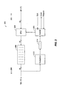
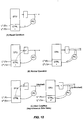
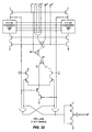
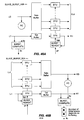
- Fig. 1 is a simplified block diagram illustrating an exemplary interface 100 for transferring data tokens from an asynchronous domain 102 to a synchronous domain 104 according to a specific embodiment of the invention.
- a 32-bit wide data token i.e., L[0..31], encoded using 1 of 2 encoding is assumed.
- data tokens having any number of bits and encoded in many different ways may be transferred from one domain to the other according to the described embodiment.
- the 32-bit wide datapath includes a multi-stage buffer queue 106 which receives and transfers the data tokens generated in the asynchronous domain from one stage to the next according to the delay-insensitive handshake protocol described above.
- buffer 106 is shown having 8 stages, i.e., being capable of accommodating 8 data tokens, it will be understood that according to various embodiments, the length of this buffer may vary. As the transfer of each data token into buffer 106 is achieved, completion of the transaction for each of the bits is signaled backwards by the first stage of buffer 106 in accordance with the handshake.
- the datapath also includes one or more asynchronous-to-synchronous (A2S) datapath transfer units (one for each bit of the data token) represented by DTU block 108.
- A2S asynchronous-to-synchronous
- DTU 108 effects the transfer of each data token to synchronous domain 104 in response to an A2S "go" signal and the clock signal (CLK) associated with synchronous domain 104.
- CLK clock signal
- completion block 110 In response to the indication that each of the bits of the token has been successfully transferred to buffer 106 (i.e., the completed handshake), completion block 110 generates a 1 of1 transfer token representing the completed transfer.
- completion block 110 employs a pipelined architecture to minimize the impact of the latency inherent in generating a single transfer token from the completion signals for each of the bits of the data token. A specific implementation of such a completion block is described below.
- control block 112 which, in turn, generates a request signal to the synchronous domain indicating that valid data are available to be transferred.
- control block 112 Upon receiving a grant signal from the synchronous domain and in response to a transition of the clock signal, control block 112 generates the A2S "go" signal which causes DTU block 108 to simultaneously latch all of the bits of the data token currently at the end of buffer 106 to the synchronous domain.
- the grant and request signals may be omitted, the A2S "go" signal being generated in response to the transfer token and the clock signal.
- distribution of the A2S "go" signal among the individual datapath transfer units in DTU 108 is accomplished using a pipelined tree structure which minimizes the effect of the latency inherent in such a distribution.
- the A2S "go" signal is distributed to the individual datapath transfer units using an electrically continuous conductor, e.g., a single wire.
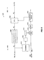
- Fig. 2 is a simplified block diagram illustrating an interface 200 for transferring data tokens from a synchronous domain 202 to an asynchronous domain 204 according to another specific embodiment of the invention.
- an exemplary 32-bit wide data token i.e., L[0..31]
- Data tokens generated in the synchronous domain are transferred to the asynchronous domain via a datapath which includes a plurality of synchronous-to-asynchronous (S2A) datapath transfer units (shown as DTU 206) and a multi-stage buffer queue 208.
- S2A synchronous-to-asynchronous
- Buffer 208 receives and transfers the data tokens received from DTU 206 from one stage to the next according to the delay-insensitive handshake protocol described above. And although buffer 208 is shown having 8 stages, i.e., being capable of accommodating 8 data tokens, it will be understood that according to various embodiments, the length of this buffer may vary. Data tokens generated in the synchronous domain are transferred into buffer 208 by DTU 206 in response to an S2A "go" signal generated by control block 210. Generation of this S2A "go" signal is described below.
- completion block 212 In response to the indication that each of the bits of the data token at the end of buffer 208 has been successfully transferred out of buffer 208, completion block 212 generates a 1 of 1 transfer token representing the completed transfer and the fact that room is now available in buffer 208 for at least one additional data token.
- completion block 212 employs a pipelined architecture to minimize the impact of the latency inherent in generating a single transfer token from the completion signals for each of the bits of the data token. A specific implementation of such a completion block is described below.
- the transfer token generated by completion block 212 is received and transferred through the stages of transfer token buffer 214 (which can accommodate multiple tokens) according to the delay-insensitive handshake protocol.
- the number of tokens in token buffer 214 at any given time corresponds to the number of available spaces in buffer 208 for additional data tokens to be transferred from the synchronous domain.
- the length of token buffer 214 may vary according to different implementations, different buffer lengths being more suitable for particular datapath widths.
- control block 210 When control block 210 receives a transfer token from buffer 214 and there is an outstanding request from the synchronous domain for transfer of a data token, control block 210 generates a grant signal indicating that the asynchronous domain is ready to receive the data token. Control block 210 also generates the S2A "go" signal which enables the transfer of the data token by DTU 206 to the first stage of buffer 208. According to a specific embodiment, the S2A "go" signal is distributed among the individual datapath transfer units of DTU 206 using a pipelined tree structure which minimizes the effect of the latency inherent in such a distribution. According to an alternative embodiment, the S2A "go” signal is distributed to the individual datapath transfer units using an electrically continuous conductor, e.g., a single wire.
- an electrically continuous conductor e.g., a single wire.
- the pipelining of the various elements which generate and distribute the "go" signals results in a low latency solution by which large data tokens may be transferred between asynchronous and synchronous domains.
- the latency for large datapaths e.g., 32 or 64-bit, can be as little as one clock period.
- burst mode interfaces solutions are provided which ensure that the data transmission requirements of the synchronous domain are satisfied.
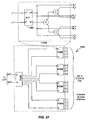
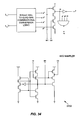
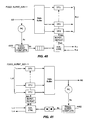
- Fig. 3 is a simplified diagram illustrating an exemplary "burst mode" interface 300 for transferring data tokens from an asynchronous domain 302 to a synchronous domain 304 according to a specific embodiment of the invention in which the synchronous domain expects data to be transmitted in uninterrupted blocks or "bursts" of consecutive tokens.
- asynchronous may be used with respect to certain circuitry, the nature of the interfaces of the present invention mean that timing constraints exist on the asynchronous side, e.g., the buffer must be fast enough to feed one data token per clock cycle. While this is a fairly easy constraint to meet in that such a buffer feeds tokens through significantly faster than the typical clock cycle, it is a constraint nevertheless.
- synchronous domain 304 is a synchronous memory architecture and interface 300 is a "write" interface. It should be understood, however, that a burst mode interface designed according to the invention is more generally applicable than the specific implementation shown in Fig. 3 . That is, various implementation details shown in Fig. 3 may not be necessary or may be replaced with other details for burst mode interfaces designed for other applications.
- a 32-bit wide data token i.e., L[0..31], encoded using 1 of2 encoding is assumed.
- Control information associated with the data token e.g., a write command bit and the address to which the data are to be written, is split off from the data token and transmitted via control path 303.
- the 32-bit data tokens are transmitted via data path 305.
- the nature of the control information will depend upon the type of memory architecture in the synchronous domain.
- the data tokens may include dummy tokens where only specific words in a block of memory are to be written. These dummy tokens may be included in the bursts and may be identified, for example, by a mask bit associated with each of the tokens.
- the 32-bit wide datapath includes a multi-stage buffer queue 306 which receives and transfers the data tokens generated in the asynchronous domain from one stage to the next according to the delay-insensitive handshake protocol described above.
- buffer 306 is shown having 24 stages, i.e., being capable of accommodating 24 data tokens, it will be understood that according to various embodiments, the length of this buffer may vary. As the transfer of each data token into buffer 306 is achieved, completion of the transaction for each of the bits is signaled backwards by the first stage of buffer 306 in accordance with the handshake.
- the datapath also includes a plurality of asynchronous-to-synchronous (A2S) datapath transfer units (one for each bit of the data token) represented by DTU block 308.
- DTU 308 effects the transfer of each data token to synchronous domain 304 in response to an A2S "go" signal and the clock signal (CLK) associated with synchronous domain 304.
- A2S "go" signal is generated according to a specific embodiment of the invention.
- completion block 310 In response to the indication that each of the bits of a token has been successfully transferred to buffer 306 (i.e., the completed handshake for each bit), completion block 310 generates a 1 of 1 transfer token representing the completed transfer.
- completion block 310 employs a pipelined architecture to minimize the impact of the latency inherent in generating a single transfer token from the completion signals for each of the bits of the data token. A specific implementation of such a completion block is described below.
- buffer 306 is implemented as a series of asynchronous stages each of which receives and transmits one 32-bit data token at a time via intervening buffer channels using the four-phase asynchronous handshake described above.
- each buffer stage comprises 16 buffer elements in parallel, each of which is responsible for receiving and transmitting two bits of the data using the handshake.
- buffer 306 and its buffer stages may be implemented without departing from the scope of the invention.
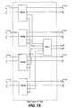
- completion block 310 employs a pipelined architecture to minimize the impact of the latency inherent in generating a single transfer token from the completion signals for each of the bits of the data token. More specifically, completion block 310 is implemented as a tree structure which generates the transfer token from a copy of the data token sent to buffer 306. An example of such a tree structure, including the circuit to copy the data token, is shown in Fig. 4 .
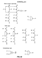
- Each buffer element 402 receives and transmits two bits of data using an asynchronous handshake protocol. Each buffer element also generates a completion signal, e.g., a copy of the enable, when a successful transfer has occurred. This completion signal (along with three other completion signals for adjacent buffer elements) is received by a 4-way token collection circuit 404 which generates a single token when all four completion signals are received. This token (along with three others generated by similar circuits 404) are transmitted to a final 4-way token collection circuit 406 which generates the transfer token in much the same way.
- the CSP for an exemplary 4-way token collection circuit which may be used in such an implementation is given by * [ ⁇ ⁇ i : 0..3 : L [ i ] ? > ; R ! ].
- the CSP for an exemplary transfer buffer element which may be used in such an implementation is given by * [ L ? x ; R ! x, T !].
- the transfer token is received by accumulator block 312 which generates a single synchronization token when a specific number of transfer tokens have been accumulated indicating the presence of at least one burst of data in the buffer; e.g., if each data token is a single word of data and a burst must be 8 words of data, a synchronization token is generated for every 8 transfer tokens received.
- Synchronization buffer 314 is simply a buffer which copies its inputs to its outputs but won't let the control information on control path 303, e.g., the address and write command, through until it receives the synchronization token from accumulator block 312 which indicates that sufficient data are present in buffer 306 to effect a write to the address identified by the control information.
- the control information is then transmitted to A2S interface 316 which may comprise a simple buffer stage similar to the datapath transfer units of DTU block 108 and 308 described above. Alternatively, A2S interface 316 may be implemented using something more elaborate such as, for example, A2S interface 100 of Fig. 1 .
- the synchronization token generated by accumulator block 312 is distributed to the individual buffer elements of synchronization buffer 314 using a pipelined tree structure, a portion of which is shown in Fig. 5 .
- tree structure 500 minimizes the impact of the latency inherent in distributing copies of a single token to each of the buffer elements.
- a 4-way token copy circuit 502 receives the synchronization token and copies the token to each of a plurality of subsequent token copy circuits 504 (which may have different numbers of outputs, e.g., 2-way, 3-way) until there are a sufficient number of copies to distribute to the individual buffer elements 506 of synchronization buffer 314.
- the CSP for an exemplary 4-way token copy circuit which may be used in such an implementation is given by * [ L ? ; ⁇ ⁇ ; : 0..3 : R [ i ] ! > ].
- the CSP for an exemplary synchronization buffer element which may be used in such an implementation is given by * [ L ? x , T ? ; R ! x ].
- the A2S "go" signal is asserted by synchronous control circuitry 318 and, in response to the successive clock signals, DTU block 308 transfers a burst of data tokens to be written to the specified memory locations according to the protocol by which the synchronous memory architecture is characterized. When the burst is complete, the "go" signal is deasserted.
- Fig. 6 is a simplified diagram illustrating an exemplary "burst mode" interface 600 for transferring data tokens from a synchronous domain 602 to an asynchronous domain 604 according to a specific embodiment of the invention.
- synchronous domain 602 comprises a synchronous memory architecture
- interface 600 is the read interface for use with the write interface of Fig. 3 .
- S2A interfaces similar to interface 600 may be employed in any of a wide variety of contexts in which the synchronous domain is required to transfer data in bursts of consecutive tokens.
- the datapath includes a plurality of synchronous-to-asynchronous (S2A) datapath transfer units (one for each bit of the data token) represented by DTU block 606.
- S2A synchronous-to-asynchronous
- DTU block 606 effects the transfer of each data token to asynchronous domain 604 in response to an S2A "go" signal and the clock signal (CLK) associated with synchronous domain 304.
- S2A "go" signal is generated according to a specific embodiment of the invention is described below.
- the 32-bit wide datapath also includes a multi-stage buffer queue 608 which receives and transfers the data tokens from one stage to the next according to the delay-insensitive handshake protocol described above.
- Buffer 608 is shown having 24 stages because in a particular embodiment, this provides space for three 8-token bursts of data. However, it will be understood that according to various embodiments, the length of this buffer may vary. As the transfer of each data token out of buffer 608 is achieved, completion of the transaction for each of the bits is signaled backwards in accordance with the handshake.
- control information e.g., a read command and address range
- asynchronous domain 604 is not transmitted into synchronous domain 602 until there is sufficient room in buffer 608 to accept the expected burst of consecutive data tokens.
- the size of the bursts are constant.
- the size of the bursts vary and may be determined with reference to the control information.
- interface 600 is configured to ensure that whatever the size of the data transfer from the synchronous domain there is sufficient buffer space to accommodate it.
- completion block 610 employs a pipelined architecture to minimize the impact of the latency inherent in generating a single transfer token from the completion signals for each of the bits of the data token. More specifically, completion block 610 may be implemented as tree structure which generates the transfer token from the completion signals generated by the asynchronous circuitry subsequent to the final stage of buffer 608. Alternatively, completion block 610 may comprise its own buffer stage following buffer 608. An example of such a tree structure is described above with reference to Fig. 4 .
- the transfer token generated by completion block 610 is received by accumulator block 612 which generates a single synchronization token when a specific number of transfer tokens have been accumulated indicating there is space in buffer 608 for at least one burst of data; e.g., if each data token is a single word of data and a burst is 8 words of data, a synchronization token is generated for every 8 transfer tokens received.
- the synchronization tokens generated by accumulator block 612 are stored in a token buffer 614 for application to synchronization buffer 616.
- Token buffer 614 is shown as being able to accommodate 3 synchronization tokens at a time. This corresponds to the number of data bursts which may be accommodated by buffer 608. However, it will be understood that token buffer 614 may vary in length along with buffer 608 without departing from the scope of the invention. ⁇ Are there any timing assumptions associated with the length chosen for the token buffer or is it dictated by the number of bursts which can be accommodated by buffer 608. It will also be understood that when the interface is powered up, token buffer 614 is fully populated with synchronization tokens to reflect the fact that buffer 608 is completely empty.
- Synchronization buffer 616 is simply a buffer which copies its inputs to its outputs but won't let the control information on control path 605, e.g., the address range and read command, through until it receives the synchronization token from token buffer 614 which indicates that sufficient space exists in buffer 306 to effect a read of data from the address range identified by the control information.
- the control information is then transmitted to A2S interface 618 which may comprise a simple buffer stage similar to the datapath transfer units of DTU block 108 and 308 described above. Alternatively, A2S interface 618 may be implemented using something more elaborate such as, for example, A2S interface 100 of Fig. 1 .
- interface 600 is configured such that each time synchronization buffer 616 receives a synchronization token from token buffer 614 any data tokens in buffer 608 have migrated far enough toward the end of the buffer such that there is sufficient space at the beginning of the buffer to accommodate the burst of data precipitated by transmission of the synchronization token. According to a specific embodiment, this may be achieved, at least in part, because of the speed with which buffer 608 transfers tokens from stage to stage.
- each synchronization token transmitted from token buffer 614 is distributed to the individual buffer elements of synchronization buffer 616 using a pipelined tree structure as discussed above with reference to Fig. 5 .
- the A2S "go" signal is asserted by synchronous control circuitry 620 and, in response to the successive clock signals, DTU block 606 transfers a burst of data tokens from synchronous domain 602 to buffer 608.
- the "go" signal is deasserted. Generation of such a "go” signal will be described below with reference to more specific embodiments.
- an asynchronous channel refers to a 1 ofN channel plus a handshaking "enable” wire.
- the enable wire is identified by an “e” superscript. Communication on these wires happens according to the asynchronous four-phase handshake protocol discussed above.
- Value refers to the state of the 1 ofN channel. When one rail is high, the channel is said to be “valid”. Otherwise, it is said to be “neutral” or invalid.
- a “token” is an abstraction referring to the propagation of valid states from one asynchronous channel to the next in a system.
- the converter designs described below also make use of a pair of synchronous handshaking signals (referred to as S° and S') to implement flow control.
- the handshake protocol used is the following: On a rising clock edge, if both A and B are high, the receiver reads the data. If A is high and B is low, the data channel contains an unread value, and the sender is waiting for the receiver to raise B. If A is low and B is high, the data channel is "empty". The receiver has read any previous value and is ready for the next one. If A and B are both low, the channel is empty and the receiver is not ready to read from the channel value.
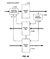
- Each of the embodiments described below implement high-performance conversion circuitry between clocked (synchronous) logic and locally-handshaking, (asynchronous) logic.
- asynchronous the transfer of data occurs on 1 ofN rail channels, following a four-phase local handshaking protocol.
- transfer of data happens according to timing relationships with the transitions of a clock signal. Any circuit which mixes the two communication conventions inevitably introduces metastability to the system. Localizing that metastability to a single signal per data token transfer while maintaining low-latency, high-throughput transfers is an objective of various embodiments described hereinafter.
- A2S Asynchronous-to-Synchronous
- S2A Synchronous-to-Asynchronous
- a simplified description of the behavior of A2S interface 802 is as follows:
- both S2A and A2S directions can sustain one transfer per clock cycle.
- the maximum latency penalty of the conversion is one clock cycle (relative to a synchronous-to-synchronous transfer), suffered only in pathological cases.
- Completion of incoming A2S and outgoing S2A tokens is pipelined (with local DI handshakes) to keep cycle times low.
- minimized synchronization to CLK allows "overclocking": correctness is maintained even as Tclk drops below its minimal value ("nop" cycles are introduced via synchronous handshaking). Assuming all timing races are met, the only possibility of metastability propagating beyond the arbiter is if the arbiter resolves during a period of one transition exactly Tclk/2 following CLK+.
- Each interface includes four high-level components:
- a token (comprising N 1 ofM channels following the four-phase handshake protocol) enters A2S converter 802 and is immediately copied to two branches: one into Pipelined Completion (PC 902), and the other into datapath buffers 912 preceding the A2S DTU array.
- PC 902 condenses the token into a single 1 of1 token through several stages of logic, the number of stages depending on the size of N and M.
- the 1 of1 token (on the " A c " channel in Fig. 9 ) is then presented to A2S CTRL process 904 as a notification that an asynchronous token has arrived and is ready to be converted.
- A2S CTRL process 904 samples the state of the 1 of1 A c channel on the next rising edge of CLK. Seeing that it contains valid data (A c d asserted), it makes the decision whether to transfer the token to the synchronous domain or not, depending on the states of the output channel and the synchronous "grant" (R e ) signal. If the R channel is empty (R v low) or if the grant signal is high, A2S CTRL process 904 will raise its request signal (R v ). If R e is also high, CTRL 904 will assert the "go" datapath signal to the DTU array indicating that the datapath transfer units should acknowledge the asynchronous data token and latch the value to the synchronous R d bits. By this time, the asynchronous token will have propagated through buffer 912 and will be ready for consumption by the array of DTUs 908.
- A2S CTRL process 904 does not transfer the token, i.e., if R v was high and R e was low, then it will neither acknowledge the A c token nor assert "go". On some subsequent clock cycle when R e goes high (indicating the recipient has accepted the stale synchronous value on R), it will then transfer the asynchronous token as described above.
- S2A CTRL process 906 decides whether to grant a transfer or not by sampling the state of the 1 of1 A c token at the rising edge of CLK. The presence of a token on A c indicates space in datapath output buffer 914 for an additional token. In this case (when A c d is set at the rising edge of CLK), S2A CTRL 906 will set its L e grant line high and acknowledge the A c token. If both L e and L v go high, the "go" signal to the array of DTUs 910 is asserted to transfer the synchronous input value to the asynchronous capture buffer.
- S2A converter 804 must satisfy the same three general categories of timing requirements described above with reference to A2S converter 802. Namely:
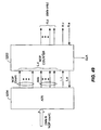
- Pipelined Completion unit 902 includes a validity detection element per input channel.
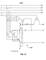
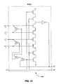
- An example of such a circuit is PCS0 1300 of Fig. 13 which has a 1 of4 input.
- PCS0 1300 is followed by a log(N)-deep tree of cells, an example of which is PCS1 cell 1400 of Fig. 14 .
- PCS0 unit 1300 implements the simple CSP specification: * L ? x ; R ! x , V !
- the "R!x" output operation is done in a "slack-zero" manner, i.e., the L and R data rails are wired together. When one of the L data rails goes high, a 1 of1 token is sent on V.
- a four-input PCS 1 unit 1400 implements the CSP specification: * [ L 0 ? , L 1 ? , L 2 ? , L 3 ? ; R ! ] i.e., it reads the 1 of1 inputs from four PCS0 units, and then outputs a single 1 of1 token.
- the PCS 1 units can be combined in a tree structure to complete arbitrarily large datapaths. Larger completion trees can be constructed in an analogous manner.
- FIG. 16 An exemplary CTRL process is shown in Fig. 16 .
- the CSP specification of either of the A2S and S2A control processes is the following:
- the "S°” output maps to the R v validity signal in the A2S converter.
- the S2A converter maps to the L e enable signal.
- the "S i " is the input R e and in the S2A converter it is L v .
- the assertion of S° can be considered to indicate the presence of a token in the control process. For the A2S converter, it indicates that the converter has asserted a data token to be consumed by the synchronous circuitry; for the S2A converter, it indicates that the converter is ready to consume a data token.
- the control process probes the input asynchronous channel A c and sets the internal variable "a" high if the channel is ready to be read.
- the process also latches its synchronous input (S'). If A c has valid data (a), or if the synchronous side is not ready (S i low), then xso (to become S°) is set high. If A c does not have valid data (-a) and the synchronous side is ready, then xso is set low. In all other cases, xso (S°) is left in its prior state.
- a c has valid data and either S' is high or S° is low, the A c token is consumed. This can happen when either S° was asserted (indicating ownership of a token in the CTRL process) and S' was high (indicating the consumption of that token on the clock cycle in question), or when S° was not asserted (indicating that the CTRL process can accept an A c token regardless of the synchronous side's state.) In this case of the logic, the process lowers the A c e signal, it waits for A c d to be deasserted, and then it re-asserts A c e .
- the "go" signal is combinationally generated as the conjunction of S i and S o .
- the datapath sees an asserted "go", and a data token passes from one domain to the other.
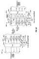
- the circuit implementation of the control process includes five components: internal completion logic 1602 responsible for sequencing the enable signal, arbitration logic 1604, S' input latching circuitry 1606, S° output control and state logic 1608, and the A c acknowledge logic 1610.
- en Central to the design of the control process is the internal enable signal ("en"), which triggers the set (en high) and reset (en low) phases of the internal dynamic logic. "en” is not strictly synchronized to CLK. It will cycle once per clock cycle, but “en” is sequenced by the validities if the internal signals, not CLK. A specific circuit implementation of the internal completion logic 1700 is shown in Fig. 17 .
- Arbiter 1802 shown in this circuit can be any standard mutual exclusion element such as, for example, a Seitz arbiter or a QFR.
- the "a" variable is implemented as a dual-rail signal pair to allow the use of domino pull-down logic stages elsewhere in the circuit. Doing so facilitates the synchronized-QDI (quasi-delay insensitive) design style used throughout the converters.
- the kc signal in this logic is used to disable the arbitration logic's clock grant signal (A g 0 ) once the A c d input wins the arbitration (A g 1 asserted). This must be done to protect the rest of the circuit from seeing a glitch on A g 0 in the case that A c e transitions negative while CLK and en are still high.
- a more specialized arbitration circuit 1900 which incorporates the kc function into a variant of the Seitz arbiter is given in Fig. 19 .
- This design removes the need for an extra dynamic logic stage to generate a.
- the series combination "A g 1 & CLK” must be included instead (i.e., requiring an extra transistor).
- the circuits in Figs. 18 and 19 limit the metastability hazard to the case that an arbiter output resolves exactly as CLK transitions negative.
- a g 1 wins A g 1 transitioning high as CLK transitions low can cause an unstable voltage on a 1 (or whatever logic stage depends on A g 1 ).
- a g 0 wins A g 0 transitioning high as CLK transitions low can cause A g 0 to return low before it has completely pulled down a 0 (or some other logic stage in the more specialized design.) In either case, the metastable condition propagates beyond the arbiter.
- the S' input signal is captured using an edge-triggered, self-disabling single-rail to dual-rail circuit 2000 shown in Fig. 20 .
- the en signal is used to set and reset the s i ⁇ 0,1 ⁇ input rails and facilitates the use of asynchronous self-sequencing logic throughout the control process.
- the design relies on this latch's synchronizing relationship to the rising edge of CLK to keep the process from repeatedly cycling in a subtle case of the logic (when the clock period is significantly slower than the A c cycle time).
- the protection comes from the circuit's property that, once en transitions low and s i resets, the s i 0 and s i 1 rails remain low until the next rising edge of CLK.
- the s i v signal encodes the validity of the s i ⁇ 0,1 ⁇ rails. It is used in the internal completion logic to allow safe, delay-insensitive sequencing of en.
- FIG. 21 A specific implementation of a S° synchronous output control circuit 2100 is shown in Fig. 21 . Since the control process must know the value of S° from the prior clock cycle, an asynchronous state element (i.e., STATEBIT circuit 2102) is used. A specific implementation of STATEBIT circuit 2102 is shown in Fig. 22 . The STATEBIT circuit provides automatic sequencing of the s o 0 and S o 1 signals over the unit's internal cycle. An alternative design might use an additional input latch of Fig. 20 to resample the state from the synchronous S° signal, but such a design would require additional circuitry to complete the S o terms in the sequencing of en.
- STATEBIT circuit 2102 A specific implementation of STATEBIT circuit 2102 is shown in Fig. 22 .
- the STATEBIT circuit provides automatic sequencing of the s o 0 and S o 1 signals over the unit's internal cycle.
- An alternative design might use an additional input latch of Fig. 20 to resample the state from
- the cross-coupled NANDs and output latch of Fig. 21 provide a safe synchronization of the asynchronous s o terms, which only pulse low during the en rising edge phase of the control process.
- the cross-coupled NANDs convert the pulse to a persistent value, and the output latch restricts the S° output from transitioning while CLK is high. Since only one of s o 0 or s o 1 can transition low at a time, and can only transition low while CLK is high, S° is set in an entirely synchronous manner.
- the s o v signal encodes the validity of the s i state logic.
- the assertion of S o v additionally implies that the cross-coupled NANDs have successfully captured the appropriate s o ⁇ 0,1 ⁇ value.
- FIG. 23 A specific implementation of an A c Acknowledge logic circuit 2300 is shown in Fig. 23 .
- This circuit is a relatively straightforward dynamic logic stage, encoding the "a & (si
- "a" is set (meaning "A g 1 & CLK") and s i 1 or S o 0 is asserted, the ack 1 rail is pulled low, causing A c e to go low, acknowledging the A c input token.
- the kc term is included in the A c e sequencing to ensure that it has disabled the arbiter's clock selection by this time (to avoid the potential glitch on A g 0 when A c d goes low in response to the falling edge of A c e ).
- the s o 1 term is redundantly included in the ack 1 pull-down to prevent the repeated cycling scenario described above in the S i input latch section.
- the ack v like the s i v and s o v signals, encodes the completion state of this block of logic.
- ack 0 When ack 0 is selected, the ack v is delayed until the falling edge of CLK by including CLK in the pull-up; when ack 1 is selected, ack v additionally completes the A c e negative transition.
- ack v does not return low until A c d has been withdrawn (completed by the A g 1 term in the ack 1 pull-up) and A c e has returned to its asserted state.
- the A2S and S2A datapath transfer units are single-channel converter elements which transfer tokens based on the value of their synchronous "go" input at various phases of the clock period.
- timing assumptions must be made on the asynchronous handshake transitions. For example, when the A2S DTU sees an asserted "go”, it must also receive a token on its L input during that clock cycle.
- the S2A DTU receives an asserted "go" its R e must be high and ready to transition low once an R data rail is asserted.
- the high-level architecture of the A2S and S2A converters ensures that these assumptions are satisfied.
- the A2S datapath transfer units have the following CSP specification:
- This process transfers the asynchronous L input to the synchronous R output on every cycle that "go" is asserted.
- the unit makes the assumption that go transitions high sometime following the falling edge of CLK but sufficiently before next rising edge of CLK to satisfy the setup time constraints of the recipient synchronous logic.
- CLK transitions high on a cycle when go is asserted L is acknowledged.
- FIG. 24 A circuit implementation of an exemplary A2S data transfer unit 2400 for a single 1 of 2 input is shown in Fig. 24 .
- the data bit latch of R is transparent when CLK is low and go is high. When go is low, R is kept low to protect the output from transitioning unpredictably when L arrives.
- the L e negative transition is conditioned on the rising edge of CLK, and the L e positive transition is conditioned on the falling edge of CLK.
- the CSP specification of the S2A datapath transfer unit is *[[CLK]; [go -> R!L[ ] else -> skip ]; [ ⁇ CLK]]
- this unit is entirely synchronous in nature; specifically, on each clock cycle, on the rising edge of CLK, it samples its inputs and evaluates some output condition. In this case, it checks if the "go" control signal from the S2A control process is set, and, if so, writes its L bit (or bits) to the R output channel in a 1 ofN rail encoding following the four-phase handshake protocol.
- Fig. 25 shows an exemplary one-bit circuit implementation of the S2A DTU 2500. This design can easily be extended to support a two-bit input, with a 1 of4 rail output data encoding.
- the A2S converter requires at least a single stage of buffering on the datapath, following the point that L is copied to the pipelined completion (PC) circuitry.
- the need for this is primarily due to performance considerations; i.e.,. in order to allow the PC to operate in a pipelined manner, it must not be bottlenecked by tokens backing up in the datapath branch.
- the datapath is "slack matched" to the control (and completion) path.
- Another reason for buffering the asynchronous data at the input of the DTU array is to ensure that the input to the DTU elements have the correct handshake properties. Namely, the A2S DTU described above relies on its input reseting (returning to its neutral state) promptly after the falling edge of L e . This can be guaranteed by having a PCHB or PCFB buffer stage directly preceeding the DTU array.
- the S2A converter imposes a much stricter requirement for additional buffering. It needs several buffer stages between its datapath output and its output PC, as well as on the A c completion channel output of the PC.
- the A c channel buffers initializes "filled", i.e. with a number of tokens corresponding to the amount of slack available in the datapath (minus one token with which the S2A control process initializes out of reset.)
- At least two tokens must be present in the S2A datapath-to-completion loop in order to support a transfer on every clock cycle.
- One token is consumed by the S2A control process and DTU elements during a transfer. Since the asynchronous portion of the loop has non-zero latency, a second token must always be present in that branch in order to pipeline the transfers.
- both the datapath and completion branches have sufficient buffering to absorb the two tokens in the loop. If the datapath buffer capacity is insufficient, the S2A DTU output handshake will stall if the S2A's R output stalls, potentially causing metastability hazards in the datapath or lost tokens. If the completion path buffer capacity is insufficient, data tokens will be trapped in the output buffer when the synchronous side stalls. In this case, the S2A converter will not output a received R token until the next token is received by the converter, which may take an arbitrarily long amount of time.
- a final performance-related factor influences the loop token (and therefore buffering) requirements of the S2A converter.
- the forward latency through the PC becomes too great, additional tokens must be present in the loop to keep the pipeline at peak capacity.
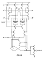
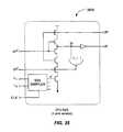
- FIG. 26 The internal high-level organization of A2S and S2A converters 2602 and 2604 according to an alternate embodiment is shown in Fig. 26 .
- Each interface includes four high-level components:
- S2A converter 2604 additionally requires extra asynchronous buffering stages 2618 between its datapath output and its output PCS, and on the "A" channel output of the PCS (i.e., buffer 2620). These provide a guarantee that any transfer initiated by an "A" token can be absorbed in the datapath if the environment is not prepared to read.
- converters 2602 and 2604 Exemplary implementation details of converters 2602 and 2604 according to specific embodiments are given below. Some elements of the designs have been omitted for clarity. These include staticizers on the output nodes of all dynamic logic, and extra reset circuitry which any practical implementation would require. Both of these additions are straightforward to implement. Other circuit details (particularly of the control processes) are not covered since there are many different solutions, and all are fairly straightforward applications of the design style described herein.
- An exemplary CSP specification of A2S control process 2608 is the following:
- S2A control process 2610 is somewhat simpler since it does not need to store the state of the synchronous datapath channel:
- Implicit in the design of these control processes is the internal enable signal ("en”), which triggers the set (en high) and reset (en low) phases of the internal dynamic logic. "en” is not strictly synchronized to CLK. It will cycle once per clock cycle (except in the case that a cycle is missed due to a maximum arbiter resolve time), but “en” is sequenced by the validities if the internal signals, not CLK (as illustrated in Fig. 28 ).
- arbiter 3202 shown in this circuit can be any standard mutual exclusion element such as, for example, a Seitz arbiter or a QFR.
- the "a" variable is implemented as a dual-rail signal pair to allow the use of domino pull-down logic stages elsewhere in the circuit. Doing so facilitates the synchronized, quasi-delay-insensitive design style used throughout the converters.
- the circuit in Fig. 29 limits the metastability hazard to the case that an arbiter output resolves exactly as CLK goes low.
- the rising edge of A g 1 as CLK goes low can cause an intermediate on a 1 .
- the rising edge of A g 0 as CLK goes low can cause A g 0 to return low before it has completely pulled down a 0 . In either case, the metastable condition propagates beyond the arbiter.
- both control processes also share an internal state variable, "x".
- both control processes use the same state variable to set their synchronous output signal, S°.
- Fig. 30 illustrates an exemplary combined statebit-to-synchronous-latch circuit.
- the "xv" signal shown in the diagram encodes the validity of the "x" variable (plus the following RS latch), needed for subsequent completion (i.e., "en” control).
- This combination of a dynamic pull-down stage ( x ) followed by an RS flip-flop, followed by a clocked latch, plus the associated xv validity circuit provides a convenient asynchronous-to-synchronous circuit fragment when the timing of x is sufficiently restricted to ensure stability of the output clocked latch. Specifically, x cannot go valid too close to the falling edge of CLK. This condition is satisfied in the CTP.
- a final shared component of the designs according to a particular embodiments is the handling of the control processes' synchronous input S i .
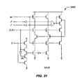
- the edge-triggered, self-disabling single-rail to dual-rail (S2DE) latch 3400 shown in Fig. 31 may be used.
- the S2DE latch provides a sufficiently safe synchronous-to-asynchronous conversion when it is possible to ensure that the rising edge of en will never coincide with the falling edge of CLK, which could cause a metastable condition on s i ⁇ 0,1 ⁇ .
- a more robust latch design (e.g., latch 3500 of Fig. 32 ) can be used to eliminate any potential metastability on s i ⁇ 0.1 ⁇ at the expense of extra transitions on its handshake cycle and an additional arbiter. These extra transitions can be hidden by inserting a buffer stage 3502 (slack 1/2) between the central control process and the S2DE latch 3400.
- CTP_A2S 2608 and CTP_S2A 2610 can be implemented in a variety of ways according to various embodiments following the general production rule synthesis techniques of the quasi-delay-insensitive design style described in "Synthesis of Asynchronous VLSI Circuits," by A.J. Martin incorporated herein by reference above. This flexibility arises from different reshuffling possibilities of the A? and go! handshaking expansions, and from different transition completion strategies. Finally, internal timing races may be introduced to simplify and/or speed up the circuits.
- L is the asynchronous input channel from the PCS
- "go” is the channel from the CTP indicating that a transfer should occur.
- the DTU_A2S reads from the L and go channels, waits for CLK to be low (note it may already be low), and then outputs the data value to the synchronous R output.
- Fig. 33 A specific circuit structure which implements the above CSP specification is given in Fig. 33 .
- the x -to-R latch and xv circuitry is identical to that used for the S o signal in the CTP circuits.
- the timing constraint on x (that it not go valid too close to the falling edge of CLK) is satisfied here.
- This implementation includes two parallel processes: one which captures the synchronous input L on every rising clock edge (and converts the single-rail data format into a 1 ofN rail format), and another which writes the value to the asynchronous output channel (R) once a "go" transfer token is received.
- N 4
- the first process can be implemented using the S2Q sampler circuit 3700 shown in Fig. 34 .
- S2Q circuit 3700 captures the values of its two synchronous inputs on every rising edge of CLK, and outputs their combined value on a 1 of4 channel, x. x transitions through its all-low state immediately following the rising edge of CLK before asserting the selected data rail. Similar circuits for N other than 4 can be implemented by changing the input combinational logic.
- the second process in this DTLJ_S2A implementation is the circuit 3800 shown in Fig. 35 . It is a WCHB stage (see “Synthesis of Asynchronous VLSI Circuits," by A.J. Martin incorporated herein by reference above) modified to accomodate its unstable x input. It treats x as an unacknowledged input, and writes its output R once go and x are valid.
- the inclusion of R 1 e in the pull-down logic (a departure from the WCHB template) provides some protection if R e and R 1 e do not transition low before the next validity phase of x (i.e., some time after the next rising edge of CLK), which might otherwise result in the assertion of multiple R rails. Doing so imposes less rigid synchronization of the transfer cycle to CLK.
- the x' rails can be excluded from the R i pull-up networks (another departure from the WCHB template) since the design guarantees that the R 1 d low-to-high transition occurs during a range of the clock cycle surrounding the falling edge of CLK, excluding the rising edge of CLK. As long as the minimum time between the rising edge of CLK and the rising edge of R 1 d is longer than the maximum x reset time (a timing assumption of the design), the unacknowledged x input poses no threat of destabilizing R.
- BUF element 3002 is a 1 of1 channel PCHB buffer.
- the CTP go d positive transition is acknowledged in three transitions instead of a minimum of seven, and the rising edge of go e can follow the falling edge of go d in a single transition compared to a minimum of seven.
- the pipelining saves 10 transitions to what would otherwise be the critical cycle of the design.
- S2A converter 2604 of Fig. 26 requires extra asynchronous buffering stages 2618 between its datapath output and its output PCS, and on the "A" channel output of the PCS (buffer 2620).
- the "A" channel buffers must initialize "filled", i.e., with a number of tokens corresponding to the amount of slack available in the datapath. This slack is defined by the number of data tokens a DTU plus its output buffers plus the PCS can hold before the go e signal would stall, i.e., not transition high following the falling edge of go d .
- At least one unit of slack (two half buffer stages) is needed between the DTUs and the PCS to ensure that the PCS can never issue an "A" token when its subsequent transfer at the datapath might stall.
- validity on the DTU output channels should not by itself result in an "A" token to be generated, since the R e 's of the DTUs (implied directly by the environment) may stall high. If a DTU's R e stalls high, its go e into the PDB stalls low. In this case, the CTP's go d transaction will not complete within a clock cycle, which the CTP_S2A specification above assumes.
- an additional unit of slack can be added to the DTU R channels and the A channel (with another initialization token). Doing so amortizes the outer loop latency over two clock cycles. The benefit of additional slack on these channels diminishes as the backward "hole" propagation latency becomes the critical cycle, incurred when the environment drains the outermost token in a full (previously stalled) state.
- the A2S and S2A converter architectures described above can be adapted to handle burst-mode transfers. It will be understood that, although one specific category of protocols is used herein to illustrate a specific implementation, various embodiments of the invention support a wide variety of burst transfer protocols. The following definitions are useful for understanding the described burst mode implementations.
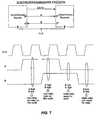
- Burst Transfer A conversion (either A2S or S2A) allowing more than one data token transfer per request/grant control handshake. For example, in implementations described above, one data token is transferred per clock cycle with both S i and S o high. By contrast, a burst transfer might transfer two, four, or any number of data tokens per clock cycle with both S i and S o high. According to a particular implementation, a maximum burst size is imposed, a constant referred to below as MAX_LEN.
- Message A sequence of data tokens.
- each data token has an associated tail bit which is zero on every data phase except the last token in the sequence.
- a message may be of arbitrary length, and the converters segment the message into bursts of lengths up to MAX_LEN.
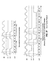
- Fig. 36 is a timing diagram which serves to illustrate such an implementation in which a message comprising data tokens DO-D9 is segmented into 3 bursts.
- Pipelined Burst Transfer A burst transfer protocol which allows the request/grant control phase of a burst transfer to take place during the transfer of a prior burst's message.
- the number of messages that the receiver will grant in advance of the communication of those messages is referred to herein as the number of grant control tokens in the sender-receiver loop. According to various embodiments, an arbitrary number of such tokens may be supported. A particular implementation imposes some finite maximum number of such outstanding granted bursts, a constant referred to as MAX_GRANT.
- Fig. 37 includes two timing diagrams, a first illustrating the signal timing for non-pipelined 3-word burst transfers, and a second illustrating signal timing for pipelined 4-word burst transfers.
- MAX_LEN a limit to the length of each message is established (MAX_LEN).
- the message length may be fixed (e.g., as shown in Fig. 37 ) or, alternatively, messages can be allowed to have a variable length up to MAX_LEN.
- a specific embodiment of a burst-mode converter designed according to the invention employs a message tail bit to support variable-length messages.
- Alternative embodiments employ other mechanisms for encoding variable message lengths (e.g., a burst count sent during the control handshake phase, or included in-band as a header word of the message).
- Alternative implementations eliminate such mechanisms where message sizes are fixed.
- Fig. 38 is a high level diagram showing such a burst mode A2S converter (BURST_A2S) 4100.
- the two new cells are burst complete logic (BURST_COMPLETE) 4102 and burst repeat cell (BURST_REPEAT) 4104.
- burst complete logic 4102 is a simple asynchronous delay-insensitive logic unit with the following CSP specification:
- the implementation of the burst complete logic varies in relation to the value of MAX_LEN.
- MAX_LEN e.g. 2 to 4.
- the cell can be implemented in a single pipeline stage with internal state bits.
- the cell may be decomposed into separate stages for incrementing the "i" internal variable and for comparing and reinitializing "i.”
- a specific circuit implementation of the burst complete logic is described below for a fixed-size message variation of a burst mode A2S converter.
- the burst repeat cell extends the "go" signal pulse to the datapath over several clock cycles corresponding to the length of the burst.
- the burst repeat cell may have the following specification:
- the burst repeat cell implements two counters: one tracking the number of outstanding bursts that have been granted by the control process (e.g., "g” incremented every time “go” is asserted within an active burst), and one tracking the length of the current active burst (e.g., "bcnt”).
- the "g” counter is required to support pipelined burst grants
- the "bcnt” counter is required to support segmentation of messages greater than MAX_LEN into multiple bursts.
- the burst repeat cell may be simplified by eliminating either or both of these features.
- burst mode A2S converter 802 of Fig. 9 Another difference in the burst mode A2S converter from the baseline A2S converter described above (e.g., A2S converter 802 of Fig. 9 ) is the amount of internal buffering on the LD and LT channels. That is, in a particular implementation of the baseline A2S converter, only a single input buffer (i.e., static slack 1) is required for correctness, although various implementations might use more for performance optimization (e.g., slack-matching to the control-to-datapath branch.) By contrast and according to a specific embodiment of the invention, for the burst mode A2S converter a single message (e.g., of MAX_LEN words) of buffering is required for correctness. Since now the control path is used only once per message, slack matching to it is less of a consideration.
- a single message e.g., of MAX_LEN words
- two requirements are placed on the message buffer:
- the burst mode A2S converter of Fig. 38 has two asynchronous input channels: the datapath LD channel (a collection of N 1 ofM channels), and an LT tail bit 1 of2 channel.
- Each data token received by the burst mode A2S converter on LD is accompanied by a tail token on LT.
- the LT token is "0.”
- the value of LT is "1.”
- the tail bit is also added to the burst mode A2S converter's synchronous output interface as another data bit (denoted "R.t" in the figure).
- LD data words enter the burst mode A2S converter, they are copied to two units: message buffer 4106 and pipeline completion (PC) unit 4108.
- message buffer 4106 stores the token until the array of data transfer units (DTUs) 4110 is ready to transfer it.
- PC unit 4108 consumes the LD token and outputs a single 1 of1 Ac token to burst complete logic 4102.
- the LT tail token associated with the LD data token is also copied to these two units: one copy is buffered with the data, and the other is sent to burst complete logic 4102.
- burst complete logic 4102 Upon receiving both Ac and LT tokens, burst complete logic 4102 either increments its internal burst counter (if LT is "0" and the counter has not reached MAX_LEN), or else it sends a 1 of1 token on its Bc output channel to A2S control unit 4112 (if LT is "1" or its counter has reached MAX_LEN).
- Control unit 4112 handles the "Bc" token just as it handles the "Ac” token in the non-burst A2S design. Namely, it asserts its "S o " handshake signal synchronously with CLK, waiting for its "S i " input to be asserted. Once both are asserted, it asserts its output "go" signal to the datapath for a single clock cycle. In the burst mode A2S converter design, the assertion of "go” represents the granting of an entire burst (up to MAX_LEN tokens) of data, rather than the single word it granted in the non-burst A2S design.
- Burst repeat cell 4104 provides the appropriate translation between the per-burst "go" signal from control unit 4112 and the per-word "bgo" control from datapath. Simply stated, it extends the single-cycle assertion of "go" over a number of cycles matching the length of the burst. In order to know when to end the burst, burst repeat cell 4104 both watches the output tail bit (i.e., R.t) and maintains an internal counter in case the message is longer than MAX_LEN (i.e., in case it must terminate the burst and continue the message over a subsequent burst when "go" is reasserted). According to an embodiment in which pipelined burst transfers are support, burst repeat cell 4104 also increments a grant counter whenever it sees an asserted "go" from control unit 4112 while a burst is still in progress.
- R.t the output tail bit
- MAX_LEN i.e., in case it must terminate the burst and continue the message over
- Fig. 39 is a high level diagram of such a burst mode S2A converter 4200 designed according to a specific embodiment of the present invention. According to a more specific embodiment, burst complete logic 4202 and burst repeat cell 4204 may be implemented as described above.
- Burst mode S2A converter 4200 has the same synchronous interface as the baseline S2A converter (e.g., S2A converter 804 of Fig. 9 ) with the addition of an L.t tail bit which can be considered an additional bit of data, its state serving to segment the data sequence on L.d into messages.
- the asynchronous output interface also remains unchanged except for the addition of the output tail bit, RT (a 1 of2 channel).
- the data output channel "R" in the baseline S2A becomes "RD" in the burst mode S2A converter.
- burst repeat cell 4204 For every burst grant cycle negotiated by L.e and L.v, up to MAX_LEN data tokens are transferred by the burst mode S2A converter's array of DTUs 4206.
- burst mode S2A converter design initializes with its data buffer completely empty and the "Bc" channel initialized with as many tokens as data buffer 4210 and burst repeat cell 4204 will support.
- the number of initial "Bc" tokens greater than one corresponds to the number of pipelined grant tokens control unit 4208 will issue.
- the internal "g" counter of burst repeat cell 4204 must support counts up to this number.
- the fixed-length burst mode A2S converter always sends MAX_LEN tokens per transfer, and the recipient synchronous logic counts the number of tokens transferred following a cycle with both S i and S o asserted to know when the message ends.
- the synchronous logic feeding a fixed-length burst mode S2A converter always provides valid data for MAX_LEN cycles beginning from a cycle with both S i and S o asserted (or following the end of the prior transfer when the control phase is pipelined).
- the asynchronous recipient logic then counts the data tokens it receives to know when messages begin or end.
- FIG. 42 An example implementation of fixed burst complete logic when MAX_LEN equals two is given in Fig. 42 (DECIMATE2_lofl).
- MAX_LEN is any power of two (2 N )
- a cascade of N DECIMATE_2_lofl units may be used to implement the fixed burst complete logic.
- MAX_LEN is not a power of two, or when the forward latency through cascaded DECIMATE2_1of1 units becomes unacceptably high, a more general counter design may be used.
- the fixed-length burst mode A2S and S2A converter designs may use the burst repeat cell described above by simply wiring the "T" tail bit input to logic zero. Alternatively, the unit may be simplified for this application by factoring out the tail bit logic from its implementation.
- DDR double data rate
- the DDR version of the A2S Datapath Transfer Unit can be specified as follows:
- the DDR version of the S2A Datapath Transfer Unit has the following specification:
- the tail bit like the synchronous handshake control signals S i and S o , remains a single-data rate signal. Each tail bit value applies to the pair of data tokens transferred on that cycle.
- A2S and S2A conversion circuits are used to implement a DDR-SDRAM interface.
- extensions to the circuits described above make such an implementation possible. These extensions include a master/slave converter system, which allows the conversion of different types of information to be linked, and a nop-counter, which can give increased performance when there are complex constraints on the minimum spacing between data items.
- the SDRAM interface uses a master/slave design in which multiple slave converters are controlled by commands sent through a "master" A2S converter. Basically, the control process of each of the slave converters is replaced with a shared mechanism that generates "go" signals for each. Based on the command word transferred, the system may also trigger one or more of the slave converters, possibly after some number of clock cycles of delay.
- the master converter is A2S.
- A2S A2S-S2A converter
- a similar system could be designed with a master S2A converter and still remain within the scope of the invention.
- the DDR-SDRAM protocol specifies that data are transferred (read or write) in a continuous burst starting a specified number of clock cycles after the corresponding read or write command. Hence the asynchronous side must ensure that data are available for writing, or empty buffer space available for reading, before issuing the associated read or write command. This requires that the converters for commands and data be linked.
- a slave A2S or S2A converter comprises a normal converter (such as any of those described above) with its control process removed.
- normal converters may comprise, for example, single-word converters (e.g., Fig. 45 ), burst converters (e.g., Fig. 46 ), or fixed burst converters (e.g., Fig. 47 ).
- Such converters may also be double data rate (DDR) converters, but are not required to be so.
- DDR double data rate
- Deleting the control process leaves the slave converter with an input signal "go" and an output completion channel Ac.
- the completion channel was called Ac for single-word converters and Bc for burst-mode converters). These channels will be referred to below as Ac for simplicity.
- a slave converter does not itself perform a synchronous handshake. Instead, it simply transfers data on every rising clock edge on which its input signal "go" is asserted. It is the responsibility of the larger system to satisfy the same conditions as are placed on the control unit of a standalone converter, i.e., to wait for a token on Ac, and perform any necessary synchronous flow control, before asserting the "go" signal.
- the Ac channel is initialized with tokens to match the amount of datapath buffering.
- Fig. 48 The general organization of an exemplary master/slave converter system is shown in Fig. 48 .
- MASTER_COMPLETE 5104 executes the following operation, specified in pseudocode, for every command:
- a SLAVE_TRIGGER unit 5106 is responsible for raising the "go" signals of the appropriate slave converters at the appropriate times, depending on the command.
- a simple version of SLAVE_TRIGGER 5106 could observe the output channel C from master A2S converter 5102. On each rising clock edge, if C is valid (C.v and C.e both high) and the command C.d indicates a slave transfer, then the corresponding slave converter is triggered through a delay line. In a particular embodiment, the delay in each delay line is programmable and corresponds to an integer number of clock periods.
- SLAVE_TRIGGER 5106 may be more complex including, for example, synchronous handshaking on the slave converters or other forms of synchronous control.
- slave converters 5108 and 5110 have more datapath buffering than their standalone counterparts. That is, in place of the control process of the standalone converter, with its relatively small latency from Ac to "go", the control latency of the slave converter passes through MASTER_COMPLETE 5104, master A2S 5102, and SLAVE_TRIGGER 5106 (with the associated delays). Therefore, the datapath buffering of the slave converter is increased to match this greater latency. The number of initial tokens on the Ac channel of slave S2A converter 5108 (representing initial empty buffer space) may be increased accordingly.
- the NOP_COLTNTER is a synchronous unit the responsibility of which is to ensure that items sent through an A2S converter are separated by at least a minimum number of clock cycles. The number is given with each item, and specifies the minimum number of skipped cycles between that item and the previous one.
- the DDR-SDRAM protocol has numerous requirements on the timing of commands which, for particular implementations, can all be expressed as minimums: before a certain command can be issued, there must have been at least a minimum number of cycles skipped (issuing null commands, or NOPs) since the previous command.
- the required number of NOPs may be generated on the asynchronous side and passed through the A2S. According to such an implementation, it would then merely be necessary for the synchronous side to generate additional NOPs when no command was available.
- the disadvantage of this approach is that it may add unnecessary delay between commands that are already widely separated. The minimum number of NOPs is not known until the following command is known, so passing those explicit NOPs through the A2S before the following command would add extra delay even though more than enough delay may have already passed.
- NOP_COLTNTER 5202 is a synchronous block attached to the output of A2S 5204. Its input and output each comprise synchronous handshake channels. The input channel carries items (commands) with an associated minimum NOP count, and the output channel sends out those same items spaced by the required number of cycles.
- CSP specification of this unit is the following:
- the SDRAM interface uses a NOP_COUNTER in conjunction with the master/slave design above.
- the NOP_COUNTER is attached to the master converter and may be considered part of the master converter for purposes of the rest of the design.
- the SLAVE_TRIGGER unit observes the output channel of the NOP_COUNTER as though it were the output of the master converter. This keeps the timing of the slave converters consistent with the command stream that emerges from the NOP_COUNTER and is visible to the other synchronous circuitry.
Landscapes
- Engineering & Computer Science (AREA)
- General Engineering & Computer Science (AREA)
- Theoretical Computer Science (AREA)
- Computer Hardware Design (AREA)
- Physics & Mathematics (AREA)
- General Physics & Mathematics (AREA)
- Information Transfer Systems (AREA)
- Communication Control (AREA)
- Synchronisation In Digital Transmission Systems (AREA)
- Pharmaceuticals Containing Other Organic And Inorganic Compounds (AREA)
Applications Claiming Priority (5)
| Application Number | Priority Date | Filing Date | Title |
|---|---|---|---|
| US212574 | 1980-12-03 | ||
| US35720102P | 2002-02-12 | 2002-02-12 | |
| US357201P | 2002-02-12 | ||
| US10/212,574 US6950959B2 (en) | 2002-02-12 | 2002-08-01 | Techniques for facilitating conversion between asynchronous and synchronous domains |
| PCT/US2003/004344 WO2003069485A2 (en) | 2002-02-12 | 2003-02-11 | Techniques for facilitating conversion between asynchronous and synchronous domains |
Publications (2)
| Publication Number | Publication Date |
|---|---|
| EP1474748A2 EP1474748A2 (en) | 2004-11-10 |
| EP1474748B1 true EP1474748B1 (en) | 2008-07-16 |
Family
ID=27737078
Family Applications (1)
| Application Number | Title | Priority Date | Filing Date |
|---|---|---|---|
| EP03711026A Expired - Lifetime EP1474748B1 (en) | 2002-02-12 | 2003-02-11 | Techniques for facilitating conversion between asynchronous and synchronous domains |
Country Status (7)
| Country | Link |
|---|---|
| US (2) | US6950959B2 (ja) |
| EP (1) | EP1474748B1 (ja) |
| JP (1) | JP4520742B2 (ja) |
| AT (1) | ATE401607T1 (ja) |
| AU (1) | AU2003215211A1 (ja) |
| DE (1) | DE60322185D1 (ja) |
| WO (1) | WO2003069485A2 (ja) |
Families Citing this family (40)
| Publication number | Priority date | Publication date | Assignee | Title |
|---|---|---|---|---|
| CN1647474A (zh) * | 2002-04-17 | 2005-07-27 | 皇家飞利浦电子股份有限公司 | 数据通信总线 |
| US7324564B2 (en) * | 2003-02-20 | 2008-01-29 | Sun Microsystems, Inc. | Transmitting odd-sized packets over a double data rate link |
| JP2004326222A (ja) * | 2003-04-22 | 2004-11-18 | Renesas Technology Corp | データ処理システム |
| US7275171B2 (en) * | 2003-05-22 | 2007-09-25 | Rambus Inc. | Method and apparatus for programmable sampling clock edge selection |
| JP4904154B2 (ja) * | 2003-07-14 | 2012-03-28 | フルクラム・マイクロシステムズ・インコーポレーテッド | 非同期スタティックランダムアクセスメモリ |
| JP3852437B2 (ja) * | 2003-11-19 | 2006-11-29 | セイコーエプソン株式会社 | 同期・非同期インターフェース回路及び電子機器 |
| US20050177660A1 (en) * | 2004-02-05 | 2005-08-11 | Rajesh Mamidwar | Method and system for merged rate-smoothing buffer with burst buffer |
| JP4956713B2 (ja) * | 2004-03-01 | 2012-06-20 | エスティー‐エリクソン、ソシエテ、アノニム | 互いに同期しない回路モジュールを備える回路 |
| ATE452371T1 (de) * | 2004-04-28 | 2010-01-15 | Koninkl Philips Electronics Nv | Schaltung mit asynchroner/synchroner schnittstelle |
| US8055821B2 (en) * | 2004-11-17 | 2011-11-08 | International Business Machines Corporation | Apparatus, system, and method for converting a synchronous interface into an asynchronous interface |
| US7584449B2 (en) * | 2004-11-22 | 2009-09-01 | Fulcrum Microsystems, Inc. | Logic synthesis of multi-level domino asynchronous pipelines |
| US7543172B2 (en) * | 2004-12-21 | 2009-06-02 | Rambus Inc. | Strobe masking in a signaling system having multiple clock domains |
| US7814280B2 (en) * | 2005-01-12 | 2010-10-12 | Fulcrum Microsystems Inc. | Shared-memory switch fabric architecture |
| JP4786354B2 (ja) * | 2006-01-27 | 2011-10-05 | 株式会社日立製作所 | iSCSI通信制御方法とそれを用いた記憶システム |
| US7668186B1 (en) * | 2006-03-07 | 2010-02-23 | Xilinx, Inc. | Token ecosystem for buffer management |
| US7610567B2 (en) * | 2006-04-27 | 2009-10-27 | Achronix Semiconductor Corporation | Systems and methods for performing automated conversion of representations of synchronous circuit designs to and from representations of asynchronous circuit designs |
| WO2007139928A2 (en) * | 2006-05-24 | 2007-12-06 | The Trustees Of Columbia University In The City Of New York | Methods, media, and means for forming asynchronous logic networks |
| WO2008008629A2 (en) | 2006-06-28 | 2008-01-17 | Achronix Semiconductor Corporation | Reconfigurable logic fabrics for integrated circuits and systems and methods for configuring reconfigurable logic fabrics |
| US7916718B2 (en) * | 2007-04-19 | 2011-03-29 | Fulcrum Microsystems, Inc. | Flow and congestion control in switch architectures for multi-hop, memory efficient fabrics |
| JP5030698B2 (ja) * | 2007-07-24 | 2012-09-19 | 株式会社リコー | 半導体装置及びノイズ低減方法 |
| US20090115488A1 (en) * | 2007-11-06 | 2009-05-07 | Jordi Cortadella | Variability-Aware Asynchronous Scheme Based on Two-Phase Protocols Using a Gated Latch Enable Scheme |
| TWI407744B (zh) * | 2008-02-04 | 2013-09-01 | Realtek Semiconductor Corp | 網路信號處理裝置 |
| JP5017153B2 (ja) * | 2008-03-14 | 2012-09-05 | 富士通株式会社 | 非同期同期通信網の変換装置、データ変換方法、データ変換プログラム、及び通信システム |
| WO2009155370A1 (en) * | 2008-06-18 | 2009-12-23 | University Of Southern California | Multi-level domino, bundled data, and mixed templates |
| US8370557B2 (en) * | 2008-12-19 | 2013-02-05 | Intel Corporation | Pseudo dual-port SRAM and a shared memory switch using multiple memory banks and a sideband memory |
| US8074193B2 (en) * | 2009-03-11 | 2011-12-06 | Institute of Computer Science (ICS) of the Foundation for Research & Technology Hellas-Foundation for Research and Technology Hellas (FORTH) | Apparatus and method for mixed single-rail and dual-rail combinational logic with completion detection |
| US8161435B2 (en) | 2009-07-20 | 2012-04-17 | Achronix Semiconductor Corporation | Reset mechanism conversion |
| US8301933B2 (en) * | 2009-09-14 | 2012-10-30 | Achronix Semiconductor Corporation | Multi-clock asynchronous logic circuits |
| US7900078B1 (en) * | 2009-09-14 | 2011-03-01 | Achronix Semiconductor Corporation | Asynchronous conversion circuitry apparatus, systems, and methods |
| US9026761B2 (en) * | 2010-12-20 | 2015-05-05 | Stmicroelectronics (Grenoble 2) Sas | Interface system, and corresponding integrated circuit and method |
| US8599982B2 (en) | 2010-12-20 | 2013-12-03 | Stmicroelectronics S.R.L. | Interface system, and corresponding integrated circuit and method |
| EP2466478B1 (en) * | 2010-12-20 | 2013-11-27 | STMicroelectronics (Grenoble 2) SAS | Communication system, and corresponding integrated circuit and method |
| FR2978315B1 (fr) * | 2011-07-20 | 2013-09-13 | Thales Sa | Reseau de transmission d'informations et noeud de reseau correspondant |
| ITTO20120289A1 (it) * | 2012-04-02 | 2013-10-03 | St Microelectronics Srl | Circuito per comunicazioni asincrone, sistema e procedimento relativi |
| GB2513529A (en) * | 2012-11-15 | 2014-11-05 | Ibm | System and method of low latency data tranfer between clock domains operated in various synchronization modes |
| US9520180B1 (en) | 2014-03-11 | 2016-12-13 | Hypres, Inc. | System and method for cryogenic hybrid technology computing and memory |
| US9558309B2 (en) * | 2014-05-09 | 2017-01-31 | University Of Southern California | Timing violation resilient asynchronous template |
| US9843339B1 (en) * | 2016-08-26 | 2017-12-12 | Hrl Laboratories, Llc | Asynchronous pulse domain to synchronous digital domain converter |
| WO2020008229A1 (en) * | 2018-07-03 | 2020-01-09 | Dolphin Integration | Circuit and method for protecting asynchronous circuits |
| CN113407467B (zh) * | 2021-07-19 | 2023-05-30 | 北京中科芯蕊科技有限公司 | 一种基于Mousetrap的同步异步转换接口及装置 |
Family Cites Families (30)
| Publication number | Priority date | Publication date | Assignee | Title |
|---|---|---|---|---|
| US4773066A (en) * | 1986-04-15 | 1988-09-20 | The Mitre Corporation | Synchronized multiple access apparatus and method for a local area network |
| US4849751A (en) * | 1987-06-08 | 1989-07-18 | American Telephone And Telegraph Company, At&T Bell Laboratories | CMOS Integrated circuit digital crossbar switching arrangement |
| US4954983A (en) * | 1987-10-13 | 1990-09-04 | Tektronix, Inc. | Data driver for multiple mode buffered processor-peripheral data transfer with selective return of data to processor |
| US5452231A (en) * | 1988-10-05 | 1995-09-19 | Quickturn Design Systems, Inc. | Hierarchically connected reconfigurable logic assembly |
| US5752070A (en) * | 1990-03-19 | 1998-05-12 | California Institute Of Technology | Asynchronous processors |
| US5418930A (en) * | 1991-09-05 | 1995-05-23 | International Business Machines Corporation | Circuit for interfacing asynchronous to synchronous communications |
| JPH0581192A (ja) * | 1991-09-18 | 1993-04-02 | Fujitsu Ltd | バスアービトレーシヨン方式 |
| JPH0784947A (ja) * | 1993-09-20 | 1995-03-31 | Hitachi Ltd | インターフェース装置 |
| JPH0784948A (ja) * | 1993-09-20 | 1995-03-31 | Hitachi Ltd | インターフェース装置 |
| JPH07249001A (ja) * | 1994-03-14 | 1995-09-26 | Hitachi Ltd | インターフェース装置 |
| US5586273A (en) * | 1994-08-18 | 1996-12-17 | International Business Machines Corporation | HDLC asynchronous to synchronous converter |
| US5659684A (en) * | 1995-02-03 | 1997-08-19 | Isdn Systems Corporation | Methods and apparatus for interconnecting personal computers (PCs) and local area networks (LANs) using packet protocols transmitted over a digital data service (DDS) |
| US5949791A (en) * | 1996-03-19 | 1999-09-07 | Lucent Technologies Inc. | Method and apparatus for converting synchronous narrowband signals into broadband asynchronous transfer mode signals in an integrated telecommunications network |
| US5802055A (en) * | 1996-04-22 | 1998-09-01 | Apple Computer, Inc. | Method and apparatus for dynamic buffer allocation in a bus bridge for pipelined reads |
| GB2313524A (en) * | 1996-05-24 | 1997-11-26 | Ibm | Providing communications links in a computer network |
| US6065082A (en) * | 1996-08-06 | 2000-05-16 | International Business Machines Corporation | HDLC asynchronous to synchronous converter |
| US5892764A (en) * | 1996-09-16 | 1999-04-06 | Sphere Communications Inc. | ATM LAN telephone system |
| US6219711B1 (en) * | 1997-05-13 | 2001-04-17 | Micron Electronics, Inc. | Synchronous communication interface |
| JP3791139B2 (ja) * | 1997-07-30 | 2006-06-28 | 株式会社デンソー | 車両用制御装置 |
| JP3488812B2 (ja) * | 1997-08-28 | 2004-01-19 | シャープ株式会社 | データ伝送路 |
| US6038656A (en) * | 1997-09-12 | 2000-03-14 | California Institute Of Technology | Pipelined completion for asynchronous communication |
| US6246733B1 (en) * | 1998-05-20 | 2001-06-12 | International Business Machines Corporation | Synchronous interface for asynchronous data detection channels |
| US6279065B1 (en) * | 1998-06-03 | 2001-08-21 | Compaq Computer Corporation | Computer system with improved memory access |
| JP2000172636A (ja) * | 1998-12-08 | 2000-06-23 | Canon Inc | リアルタイムデータ転送系の非同期系データ転送制御装置および方法 |
| US6301630B1 (en) * | 1998-12-10 | 2001-10-09 | International Business Machines Corporation | Interrupt response in a multiple set buffer pool bus bridge |
| US6374307B1 (en) * | 1999-02-12 | 2002-04-16 | Steve A. Ristau | Non-intrusive DWDM billing system |
| TW507418B (en) * | 1999-02-26 | 2002-10-21 | Via Tech Inc | Synchronization element for converting asynchronous pulse signal into synchronous pulse signal |
| US6230228B1 (en) * | 1999-04-01 | 2001-05-08 | Intel Corporation | Efficient bridge architecture for handling multiple write transactions simultaneously |
| JP3663351B2 (ja) * | 2000-02-28 | 2005-06-22 | シャープ株式会社 | 自己同期システムとクロック同期システムとのインタフェース装置 |
| US7006498B2 (en) * | 2000-08-09 | 2006-02-28 | International Business Machines Corporation | System for transmitting local area network (LAN) data frames through an asynchronous transfer mode (ATM) crossbar switch |
-
2002
- 2002-08-01 US US10/212,574 patent/US6950959B2/en not_active Expired - Lifetime
- 2002-10-25 US US10/281,424 patent/US6961863B2/en not_active Expired - Fee Related
-
2003
- 2003-02-11 EP EP03711026A patent/EP1474748B1/en not_active Expired - Lifetime
- 2003-02-11 WO PCT/US2003/004344 patent/WO2003069485A2/en active Application Filing
- 2003-02-11 AU AU2003215211A patent/AU2003215211A1/en not_active Abandoned
- 2003-02-11 DE DE60322185T patent/DE60322185D1/de not_active Expired - Lifetime
- 2003-02-11 AT AT03711026T patent/ATE401607T1/de not_active IP Right Cessation
- 2003-02-11 JP JP2003568541A patent/JP4520742B2/ja not_active Expired - Fee Related
Also Published As
| Publication number | Publication date |
|---|---|
| JP2005518018A (ja) | 2005-06-16 |
| JP4520742B2 (ja) | 2010-08-11 |
| AU2003215211A8 (en) | 2003-09-04 |
| AU2003215211A1 (en) | 2003-09-04 |
| WO2003069485A2 (en) | 2003-08-21 |
| US6950959B2 (en) | 2005-09-27 |
| ATE401607T1 (de) | 2008-08-15 |
| US20030165158A1 (en) | 2003-09-04 |
| DE60322185D1 (de) | 2008-08-28 |
| EP1474748A2 (en) | 2004-11-10 |
| US6961863B2 (en) | 2005-11-01 |
| US20030159078A1 (en) | 2003-08-21 |
| WO2003069485A3 (en) | 2004-04-01 |
Similar Documents
| Publication | Publication Date | Title |
|---|---|---|
| EP1474748B1 (en) | Techniques for facilitating conversion between asynchronous and synchronous domains | |
| EP1590835B1 (en) | Asynchronous system-on-a-chip interconnect | |
| Nowick et al. | High-performance asynchronous pipelines: An overview | |
| Mullins et al. | Demystifying data-driven and pausible clocking schemes | |
| US6308229B1 (en) | System for facilitating interfacing between multiple non-synchronous systems utilizing an asynchronous FIFO that uses asynchronous logic | |
| US5920899A (en) | Asynchronous pipeline whose stages generate output request before latching data | |
| US20020167337A1 (en) | Low latency FIFO circuits for mixed asynchronous and synchronous systems | |
| US6925549B2 (en) | Asynchronous pipeline control interface using tag values to control passing data through successive pipeline stages | |
| EP1468372B1 (en) | Asynchronous crossbar with deterministic or arbitrated control | |
| EP0826179A1 (en) | Source synchronous clocked data link | |
| US20040128413A1 (en) | Low latency fifo circuits for mixed asynchronous and synchronous systems | |
| Moore et al. | Using stoppable clocks to safely interface asynchronous and synchronous subsystems | |
| Yantchev et al. | Low-latency asynchronous FIFO buffers | |
| Verbitsky et al. | StarSync: An extendable standard-cell mesochronous synchronizer | |
| Bainbridge et al. | MARBLE: An asynchronous on-chip macrocell bus | |
| Dobkin et al. | Two-phase synchronization with sub-cycle latency | |
| Apperson | A dual-clock FIFO for the reliable transfer of high-throughput data between unrelated clock domains | |
| Elrabaa | A new FIFO design enabling fully-synchronous on-chip data communication network | |
| Verbitskyv et al. | A four-stage mesochronous synchronizer with back-pressure and buffering for short and long range communications | |
| Saxena et al. | Implementation of asynchronous pipeline using Transmission Gate logic | |
| Dobkin et al. | Fast universal synchronizers | |
| Abdelhadi et al. | Two-phase asynchronous to synchronous interfaces for an open-source bundled-data flow | |
| Dobkin et al. | Zero latency synchronizers using four and two phase protocols | |
| Maniraj | Analysis of asynchronous routers for network-on-chip applications | |
| Chakrabarti et al. | RAPPID Synchronization |
Legal Events
| Date | Code | Title | Description |
|---|---|---|---|
| PUAI | Public reference made under article 153(3) epc to a published international application that has entered the european phase |
Free format text: ORIGINAL CODE: 0009012 |
|
| 17P | Request for examination filed |
Effective date: 20040813 |
|
| AK | Designated contracting states |
Kind code of ref document: A2 Designated state(s): AT BE BG CH CY CZ DE DK EE ES FI FR GB GR HU IE IT LI LU MC NL PT SE SI SK TR |
|
| AX | Request for extension of the european patent |
Extension state: AL LT LV MK RO |
|
| GRAP | Despatch of communication of intention to grant a patent |
Free format text: ORIGINAL CODE: EPIDOSNIGR1 |
|
| GRAS | Grant fee paid |
Free format text: ORIGINAL CODE: EPIDOSNIGR3 |
|
| GRAA | (expected) grant |
Free format text: ORIGINAL CODE: 0009210 |
|
| AK | Designated contracting states |
Kind code of ref document: B1 Designated state(s): AT BE BG CH CY CZ DE DK EE ES FI FR GB GR HU IE IT LI LU MC NL PT SE SI SK TR |
|
| REG | Reference to a national code |
Ref country code: GB Ref legal event code: FG4D |
|
| REG | Reference to a national code |
Ref country code: CH Ref legal event code: EP |
|
| REF | Corresponds to: |
Ref document number: 60322185 Country of ref document: DE Date of ref document: 20080828 Kind code of ref document: P |
|
| REG | Reference to a national code |
Ref country code: IE Ref legal event code: FG4D |
|
| REG | Reference to a national code |
Ref country code: SE Ref legal event code: TRGR |
|
| PG25 | Lapsed in a contracting state [announced via postgrant information from national office to epo] |
Ref country code: PT Free format text: LAPSE BECAUSE OF FAILURE TO SUBMIT A TRANSLATION OF THE DESCRIPTION OR TO PAY THE FEE WITHIN THE PRESCRIBED TIME-LIMIT Effective date: 20081216 Ref country code: ES Free format text: LAPSE BECAUSE OF FAILURE TO SUBMIT A TRANSLATION OF THE DESCRIPTION OR TO PAY THE FEE WITHIN THE PRESCRIBED TIME-LIMIT Effective date: 20081027 |
|
| PG25 | Lapsed in a contracting state [announced via postgrant information from national office to epo] |
Ref country code: FI Free format text: LAPSE BECAUSE OF FAILURE TO SUBMIT A TRANSLATION OF THE DESCRIPTION OR TO PAY THE FEE WITHIN THE PRESCRIBED TIME-LIMIT Effective date: 20080716 Ref country code: AT Free format text: LAPSE BECAUSE OF FAILURE TO SUBMIT A TRANSLATION OF THE DESCRIPTION OR TO PAY THE FEE WITHIN THE PRESCRIBED TIME-LIMIT Effective date: 20080716 Ref country code: SI Free format text: LAPSE BECAUSE OF FAILURE TO SUBMIT A TRANSLATION OF THE DESCRIPTION OR TO PAY THE FEE WITHIN THE PRESCRIBED TIME-LIMIT Effective date: 20080716 Ref country code: BG Free format text: LAPSE BECAUSE OF FAILURE TO SUBMIT A TRANSLATION OF THE DESCRIPTION OR TO PAY THE FEE WITHIN THE PRESCRIBED TIME-LIMIT Effective date: 20081016 |
|
| PG25 | Lapsed in a contracting state [announced via postgrant information from national office to epo] |
Ref country code: BE Free format text: LAPSE BECAUSE OF FAILURE TO SUBMIT A TRANSLATION OF THE DESCRIPTION OR TO PAY THE FEE WITHIN THE PRESCRIBED TIME-LIMIT Effective date: 20080716 |
|
| PG25 | Lapsed in a contracting state [announced via postgrant information from national office to epo] |
Ref country code: DK Free format text: LAPSE BECAUSE OF FAILURE TO SUBMIT A TRANSLATION OF THE DESCRIPTION OR TO PAY THE FEE WITHIN THE PRESCRIBED TIME-LIMIT Effective date: 20080716 Ref country code: EE Free format text: LAPSE BECAUSE OF FAILURE TO SUBMIT A TRANSLATION OF THE DESCRIPTION OR TO PAY THE FEE WITHIN THE PRESCRIBED TIME-LIMIT Effective date: 20080716 |
|
| PLBE | No opposition filed within time limit |
Free format text: ORIGINAL CODE: 0009261 |
|
| STAA | Information on the status of an ep patent application or granted ep patent |
Free format text: STATUS: NO OPPOSITION FILED WITHIN TIME LIMIT |
|
| PG25 | Lapsed in a contracting state [announced via postgrant information from national office to epo] |
Ref country code: SK Free format text: LAPSE BECAUSE OF FAILURE TO SUBMIT A TRANSLATION OF THE DESCRIPTION OR TO PAY THE FEE WITHIN THE PRESCRIBED TIME-LIMIT Effective date: 20080716 Ref country code: CZ Free format text: LAPSE BECAUSE OF FAILURE TO SUBMIT A TRANSLATION OF THE DESCRIPTION OR TO PAY THE FEE WITHIN THE PRESCRIBED TIME-LIMIT Effective date: 20080716 |
|
| 26N | No opposition filed |
Effective date: 20090417 |
|
| PG25 | Lapsed in a contracting state [announced via postgrant information from national office to epo] |
Ref country code: MC Free format text: LAPSE BECAUSE OF NON-PAYMENT OF DUE FEES Effective date: 20090228 |
|
| REG | Reference to a national code |
Ref country code: CH Ref legal event code: PL |
|
| PG25 | Lapsed in a contracting state [announced via postgrant information from national office to epo] |
Ref country code: CH Free format text: LAPSE BECAUSE OF NON-PAYMENT OF DUE FEES Effective date: 20090228 Ref country code: LI Free format text: LAPSE BECAUSE OF NON-PAYMENT OF DUE FEES Effective date: 20090228 |
|
| PG25 | Lapsed in a contracting state [announced via postgrant information from national office to epo] |
Ref country code: IE Free format text: LAPSE BECAUSE OF NON-PAYMENT OF DUE FEES Effective date: 20090211 |
|
| PG25 | Lapsed in a contracting state [announced via postgrant information from national office to epo] |
Ref country code: GR Free format text: LAPSE BECAUSE OF FAILURE TO SUBMIT A TRANSLATION OF THE DESCRIPTION OR TO PAY THE FEE WITHIN THE PRESCRIBED TIME-LIMIT Effective date: 20081017 |
|
| PG25 | Lapsed in a contracting state [announced via postgrant information from national office to epo] |
Ref country code: LU Free format text: LAPSE BECAUSE OF NON-PAYMENT OF DUE FEES Effective date: 20090211 |
|
| PG25 | Lapsed in a contracting state [announced via postgrant information from national office to epo] |
Ref country code: HU Free format text: LAPSE BECAUSE OF FAILURE TO SUBMIT A TRANSLATION OF THE DESCRIPTION OR TO PAY THE FEE WITHIN THE PRESCRIBED TIME-LIMIT Effective date: 20090117 |
|
| PG25 | Lapsed in a contracting state [announced via postgrant information from national office to epo] |
Ref country code: TR Free format text: LAPSE BECAUSE OF FAILURE TO SUBMIT A TRANSLATION OF THE DESCRIPTION OR TO PAY THE FEE WITHIN THE PRESCRIBED TIME-LIMIT Effective date: 20080716 |
|
| PG25 | Lapsed in a contracting state [announced via postgrant information from national office to epo] |
Ref country code: CY Free format text: LAPSE BECAUSE OF FAILURE TO SUBMIT A TRANSLATION OF THE DESCRIPTION OR TO PAY THE FEE WITHIN THE PRESCRIBED TIME-LIMIT Effective date: 20080716 |
|
| REG | Reference to a national code |
Ref country code: DE Ref legal event code: R081 Ref document number: 60322185 Country of ref document: DE Owner name: INTEL CORPORATION, INC., US Free format text: FORMER OWNER: FULCRUM MICROSYSTEMS INC., CALABASAS, US Effective date: 20130418 Ref country code: DE Ref legal event code: R082 Ref document number: 60322185 Country of ref document: DE Representative=s name: PATENT- UND RECHTSANWAELTE KRAUS & WEISERT, DE Effective date: 20130418 Ref country code: DE Ref legal event code: R081 Ref document number: 60322185 Country of ref document: DE Owner name: INTEL CORPORATION, US Free format text: FORMER OWNER: FULCRUM MICROSYSTEMS INC., CALABASAS, US Effective date: 20130418 Ref country code: DE Ref legal event code: R081 Ref document number: 60322185 Country of ref document: DE Owner name: INTEL CORPORATION, SANTA CLARA, US Free format text: FORMER OWNER: FULCRUM MICROSYSTEMS INC., CALABASAS, CALIF., US Effective date: 20130418 Ref country code: DE Ref legal event code: R082 Ref document number: 60322185 Country of ref document: DE Representative=s name: KRAUS & WEISERT PATENTANWAELTE PARTGMBB, DE Effective date: 20130418 |
|
| REG | Reference to a national code |
Ref country code: GB Ref legal event code: 732E Free format text: REGISTERED BETWEEN 20130523 AND 20130529 |
|
| REG | Reference to a national code |
Ref country code: DE Ref legal event code: R082 Ref document number: 60322185 Country of ref document: DE Representative=s name: PATENT- UND RECHTSANWAELTE KRAUS & WEISERT, DE |
|
| REG | Reference to a national code |
Ref country code: FR Ref legal event code: TP Owner name: INTEL CORPORATION, US Effective date: 20131001 |
|
| REG | Reference to a national code |
Ref country code: DE Ref legal event code: R082 Ref document number: 60322185 Country of ref document: DE Representative=s name: PATENT- UND RECHTSANWAELTE KRAUS & WEISERT, DE Effective date: 20130927 Ref country code: DE Ref legal event code: R081 Ref document number: 60322185 Country of ref document: DE Owner name: INTEL CORPORATION, US Free format text: FORMER OWNER: INTEL CORPORATION, INC., SANTA CLARA, US Effective date: 20130927 Ref country code: DE Ref legal event code: R081 Ref document number: 60322185 Country of ref document: DE Owner name: INTEL CORPORATION, SANTA CLARA, US Free format text: FORMER OWNER: INTEL CORPORATION, INC., SANTA CLARA, CALIF., US Effective date: 20130927 Ref country code: DE Ref legal event code: R082 Ref document number: 60322185 Country of ref document: DE Representative=s name: KRAUS & WEISERT PATENTANWAELTE PARTGMBB, DE Effective date: 20130927 |
|
| REG | Reference to a national code |
Ref country code: NL Ref legal event code: SD Effective date: 20140410 |
|
| PGFP | Annual fee paid to national office [announced via postgrant information from national office to epo] |
Ref country code: SE Payment date: 20140211 Year of fee payment: 12 Ref country code: NL Payment date: 20140208 Year of fee payment: 12 |
|
| PGFP | Annual fee paid to national office [announced via postgrant information from national office to epo] |
Ref country code: FR Payment date: 20140211 Year of fee payment: 12 Ref country code: IT Payment date: 20140211 Year of fee payment: 12 |
|
| REG | Reference to a national code |
Ref country code: NL Ref legal event code: V1 Effective date: 20150901 |
|
| REG | Reference to a national code |
Ref country code: SE Ref legal event code: EUG |
|
| PG25 | Lapsed in a contracting state [announced via postgrant information from national office to epo] |
Ref country code: NL Free format text: LAPSE BECAUSE OF NON-PAYMENT OF DUE FEES Effective date: 20150901 |
|
| REG | Reference to a national code |
Ref country code: FR Ref legal event code: ST Effective date: 20151030 |
|
| PG25 | Lapsed in a contracting state [announced via postgrant information from national office to epo] |
Ref country code: SE Free format text: LAPSE BECAUSE OF NON-PAYMENT OF DUE FEES Effective date: 20150212 |
|
| PG25 | Lapsed in a contracting state [announced via postgrant information from national office to epo] |
Ref country code: IT Free format text: LAPSE BECAUSE OF NON-PAYMENT OF DUE FEES Effective date: 20150211 |
|
| PG25 | Lapsed in a contracting state [announced via postgrant information from national office to epo] |
Ref country code: FR Free format text: LAPSE BECAUSE OF NON-PAYMENT OF DUE FEES Effective date: 20150302 |
|
| PGFP | Annual fee paid to national office [announced via postgrant information from national office to epo] |
Ref country code: GB Payment date: 20170208 Year of fee payment: 15 |
|
| GBPC | Gb: european patent ceased through non-payment of renewal fee |
Effective date: 20180211 |
|
| PG25 | Lapsed in a contracting state [announced via postgrant information from national office to epo] |
Ref country code: GB Free format text: LAPSE BECAUSE OF NON-PAYMENT OF DUE FEES Effective date: 20180211 |
|
| PGFP | Annual fee paid to national office [announced via postgrant information from national office to epo] |
Ref country code: DE Payment date: 20190129 Year of fee payment: 17 |
|
| REG | Reference to a national code |
Ref country code: DE Ref legal event code: R119 Ref document number: 60322185 Country of ref document: DE |
|
| PG25 | Lapsed in a contracting state [announced via postgrant information from national office to epo] |
Ref country code: DE Free format text: LAPSE BECAUSE OF NON-PAYMENT OF DUE FEES Effective date: 20200901 |