EP1471164A1 - Copper alloy sputtering target and method for manufacturing the target - Google Patents
Copper alloy sputtering target and method for manufacturing the target Download PDFInfo
- Publication number
- EP1471164A1 EP1471164A1 EP02783764A EP02783764A EP1471164A1 EP 1471164 A1 EP1471164 A1 EP 1471164A1 EP 02783764 A EP02783764 A EP 02783764A EP 02783764 A EP02783764 A EP 02783764A EP 1471164 A1 EP1471164 A1 EP 1471164A1
- Authority
- EP
- European Patent Office
- Prior art keywords
- target
- copper alloy
- less
- alloy sputtering
- sputtering target
- Prior art date
- Legal status (The legal status is an assumption and is not a legal conclusion. Google has not performed a legal analysis and makes no representation as to the accuracy of the status listed.)
- Granted
Links
Classifications
-
- C—CHEMISTRY; METALLURGY
- C22—METALLURGY; FERROUS OR NON-FERROUS ALLOYS; TREATMENT OF ALLOYS OR NON-FERROUS METALS
- C22C—ALLOYS
- C22C9/00—Alloys based on copper
- C22C9/02—Alloys based on copper with tin as the next major constituent
-
- C—CHEMISTRY; METALLURGY
- C23—COATING METALLIC MATERIAL; COATING MATERIAL WITH METALLIC MATERIAL; CHEMICAL SURFACE TREATMENT; DIFFUSION TREATMENT OF METALLIC MATERIAL; COATING BY VACUUM EVAPORATION, BY SPUTTERING, BY ION IMPLANTATION OR BY CHEMICAL VAPOUR DEPOSITION, IN GENERAL; INHIBITING CORROSION OF METALLIC MATERIAL OR INCRUSTATION IN GENERAL
- C23C—COATING METALLIC MATERIAL; COATING MATERIAL WITH METALLIC MATERIAL; SURFACE TREATMENT OF METALLIC MATERIAL BY DIFFUSION INTO THE SURFACE, BY CHEMICAL CONVERSION OR SUBSTITUTION; COATING BY VACUUM EVAPORATION, BY SPUTTERING, BY ION IMPLANTATION OR BY CHEMICAL VAPOUR DEPOSITION, IN GENERAL
- C23C14/00—Coating by vacuum evaporation, by sputtering or by ion implantation of the coating forming material
- C23C14/22—Coating by vacuum evaporation, by sputtering or by ion implantation of the coating forming material characterised by the process of coating
- C23C14/34—Sputtering
-
- C—CHEMISTRY; METALLURGY
- C22—METALLURGY; FERROUS OR NON-FERROUS ALLOYS; TREATMENT OF ALLOYS OR NON-FERROUS METALS
- C22C—ALLOYS
- C22C19/00—Alloys based on nickel or cobalt
-
- C—CHEMISTRY; METALLURGY
- C22—METALLURGY; FERROUS OR NON-FERROUS ALLOYS; TREATMENT OF ALLOYS OR NON-FERROUS METALS
- C22C—ALLOYS
- C22C9/00—Alloys based on copper
-
- C—CHEMISTRY; METALLURGY
- C22—METALLURGY; FERROUS OR NON-FERROUS ALLOYS; TREATMENT OF ALLOYS OR NON-FERROUS METALS
- C22C—ALLOYS
- C22C9/00—Alloys based on copper
- C22C9/01—Alloys based on copper with aluminium as the next major constituent
-
- C—CHEMISTRY; METALLURGY
- C22—METALLURGY; FERROUS OR NON-FERROUS ALLOYS; TREATMENT OF ALLOYS OR NON-FERROUS METALS
- C22F—CHANGING THE PHYSICAL STRUCTURE OF NON-FERROUS METALS AND NON-FERROUS ALLOYS
- C22F1/00—Changing the physical structure of non-ferrous metals or alloys by heat treatment or by hot or cold working
-
- C—CHEMISTRY; METALLURGY
- C23—COATING METALLIC MATERIAL; COATING MATERIAL WITH METALLIC MATERIAL; CHEMICAL SURFACE TREATMENT; DIFFUSION TREATMENT OF METALLIC MATERIAL; COATING BY VACUUM EVAPORATION, BY SPUTTERING, BY ION IMPLANTATION OR BY CHEMICAL VAPOUR DEPOSITION, IN GENERAL; INHIBITING CORROSION OF METALLIC MATERIAL OR INCRUSTATION IN GENERAL
- C23C—COATING METALLIC MATERIAL; COATING MATERIAL WITH METALLIC MATERIAL; SURFACE TREATMENT OF METALLIC MATERIAL BY DIFFUSION INTO THE SURFACE, BY CHEMICAL CONVERSION OR SUBSTITUTION; COATING BY VACUUM EVAPORATION, BY SPUTTERING, BY ION IMPLANTATION OR BY CHEMICAL VAPOUR DEPOSITION, IN GENERAL
- C23C14/00—Coating by vacuum evaporation, by sputtering or by ion implantation of the coating forming material
- C23C14/22—Coating by vacuum evaporation, by sputtering or by ion implantation of the coating forming material characterised by the process of coating
- C23C14/34—Sputtering
- C23C14/3407—Cathode assembly for sputtering apparatus, e.g. Target
- C23C14/3414—Metallurgical or chemical aspects of target preparation, e.g. casting, powder metallurgy
-
- H—ELECTRICITY
- H10—SEMICONDUCTOR DEVICES; ELECTRIC SOLID-STATE DEVICES NOT OTHERWISE PROVIDED FOR
- H10P—GENERIC PROCESSES OR APPARATUS FOR THE MANUFACTURE OR TREATMENT OF DEVICES COVERED BY CLASS H10
- H10P14/00—Formation of materials, e.g. in the shape of layers or pillars
- H10P14/40—Formation of materials, e.g. in the shape of layers or pillars of conductive or resistive materials
- H10P14/42—Formation of materials, e.g. in the shape of layers or pillars of conductive or resistive materials using a gas or vapour
-
- H—ELECTRICITY
- H10—SEMICONDUCTOR DEVICES; ELECTRIC SOLID-STATE DEVICES NOT OTHERWISE PROVIDED FOR
- H10W—GENERIC PACKAGES, INTERCONNECTIONS, CONNECTORS OR OTHER CONSTRUCTIONAL DETAILS OF DEVICES COVERED BY CLASS H10
- H10W20/00—Interconnections in chips, wafers or substrates
- H10W20/40—Interconnections external to wafers or substrates, e.g. back-end-of-line [BEOL] metallisations or vias connecting to gate electrodes
- H10W20/41—Interconnections external to wafers or substrates, e.g. back-end-of-line [BEOL] metallisations or vias connecting to gate electrodes characterised by their conductive parts
- H10W20/44—Conductive materials thereof
- H10W20/4403—Conductive materials thereof based on metals, e.g. alloys, metal silicides
- H10W20/4421—Conductive materials thereof based on metals, e.g. alloys, metal silicides the principal metal being copper
- H10W20/4424—Copper alloys
Definitions
- the present invention pertains to a copper alloy sputtering target capable of forming an interconnection material of a semiconductor device, particularly a stable and even seed layer during electroplating, and superior in sputtering deposition characteristics.
- the present invention also pertains to the manufacturing method of such a target.
- a diffusion barrier layer such as Ta/TaN
- Cu electroplating is often performed thereto.
- the base layer seed layer
- sputtering deposition is generally performed to copper or copper alloy.
- this base layer is important, and, if the base layer agglomerares, an even film cannot be formed upon forming a copper film with electroplating. For instance, defects such as voids, hillocks, disconnections and so on may be formed during the wiring.
- Japanese Patent Laid-Open Publication No. H5-311424 and Japanese Patent Laid-Open Publication No. H10-60633 disclose a pure copper target or a target to which 0.04 to 0.15wt% of Ti is added to the pure copper.
- the present inventors have discovered that, as a result of adding a suitable amount of metal elements, it is possible to obtain a copper alloy sputtering target capable of preventing the generation of defects such as voids, hillocks and disconnections during copper electroplating, which has low resistivity, which has electromigration resistance and oxidization resistance characteristics, and which is able to form a stable and even seed layer.
- the present invention provides:
- the copper alloy sputtering target of the present invention contains a 0.4 to 5wt%, preferably 0.5 to 1wt% of Sn; 0.2 to 5wt%, preferably 0.5 to 1wt% of Al; 0.3 to 5wt%, preferably 0.5 to 1wt% of Ti; respectively, or a total of 0.2 to 5wt% of at least one component selected from Sn, Al and Ti.
- resistivity of the target material When 0.4 to 5wt% of Sn is independently added, resistivity of the target material will be 2.3 ⁇ ⁇ cm or more; when 0.2 to 5wt% of Al is independently added, resistivity of the target material will be 2.2 ⁇ ⁇ cm or more, and when 0.3 to 5wt% of Ti is independently added, resistivity of the target material will be 9 ⁇ ⁇ cm or more. Further, when these are mixed and added, resistivity of the target material will be 2.2 ⁇ ⁇ cm or more. These may be suitably selected and used for the formation of a seed layer during copper electroplating.
- the structure of the copper alloy sputtering target of the present invention does not substantially contain any precipitates, when the foregoing additive amount of alloy exceeds 0.2wt%, precipitates will arise during the manufacture process of the target.
- precipitates occur not during the initial phase of sputtering, but from a stage in which the erosion of the target caused by sputtering has progressed to a certain degree.
- precipitates are caused by minute particles getting mixed into the sputtering film, or due to the micro unevenness of the film composition midway during sputtering.
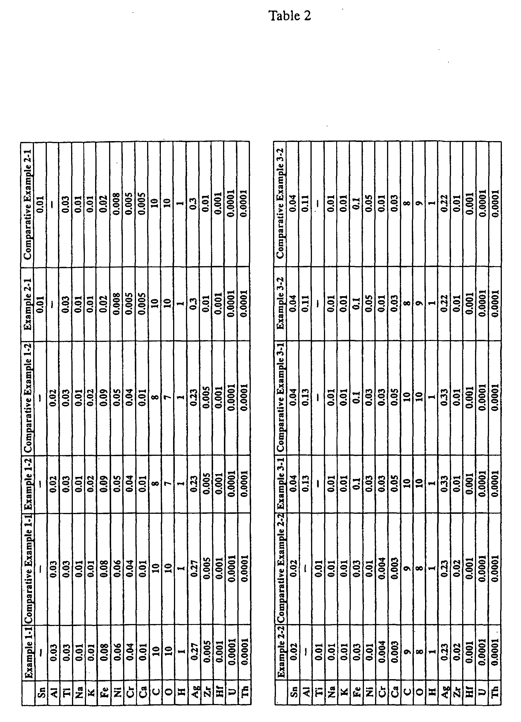
- Na and K are respectively 0.5ppm or less, preferably 0.1ppm or less; Fe, Ni, Cr and Ca are respectively 2ppm or less, preferably 1ppm or less; U and Th are respectively 1ppb or less, oxygen is 5ppm or less, hydrogen is 2ppm or less; and unavoidable impurities excluding alloying additional elements are 50ppm or less. These elements are harmful components that may diffuse and contaminate the semiconductor device.
- the crystal grain size of the target material is 50 ⁇ m or less, and the variation in the average grain size by location is within ⁇ 20%.
- the crystal grain size of the target and variations in the average grain size by location will affect the uniformity of the film thickness.
- the characteristic values of the target material will change and therefore cause the interconnection material of the semiconductor device, particularly the resistivity of the seed layer, to change, and it is desirable that the variation be within 0.2%.
- orientation of the crystal will also affect the uniformity of the film thickness. Generally, although it is considered that a random orientation is favorable, depending on the type of additive element, a specific crystal orientation with the variation being within a certain range will yield a further superior uniformity of the film thickness.
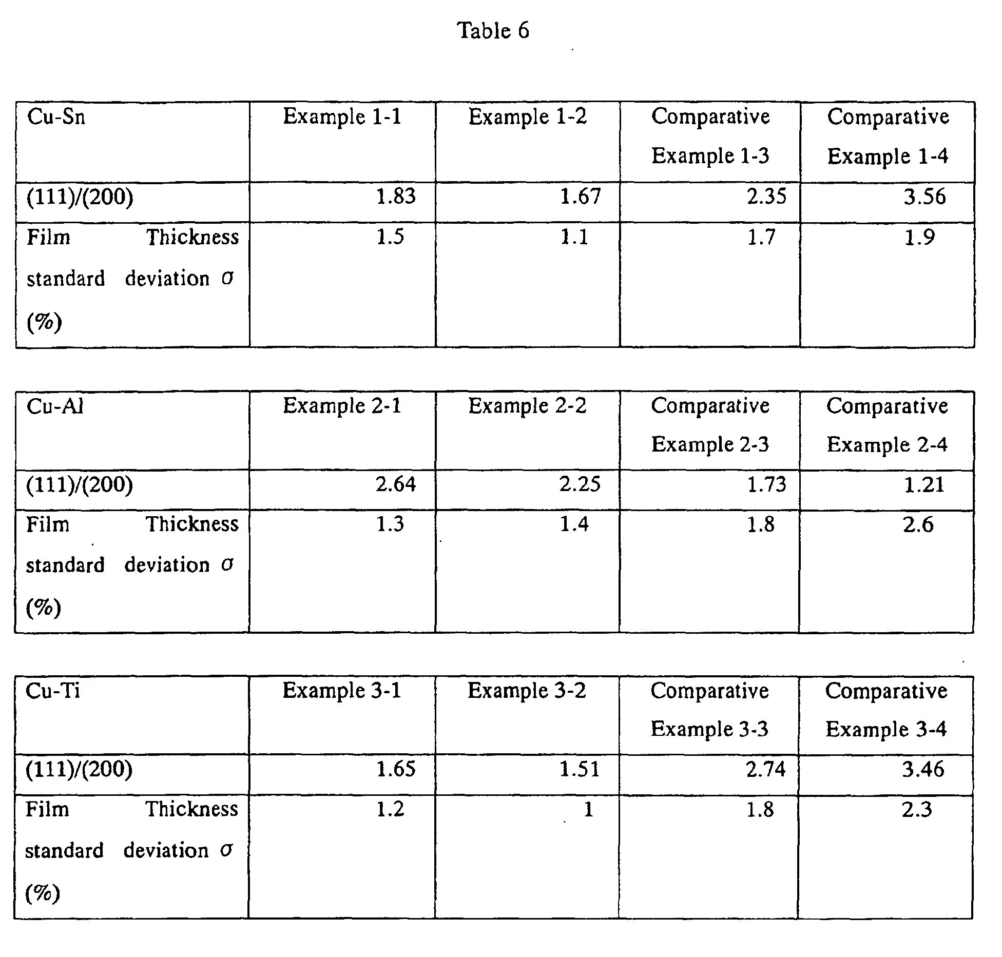
- the ratio I(111)/I(200) of the X-ray diffraction peak intensity I(111) of the (111) face and the X-ray diffraction peak intensity I (200) of the (200) face is 2.2 or more in the sputtering face
- the ratio I(111)/I(200) of the X-ray diffraction peak intensity I(111) of the (111) face and the X-ray diffraction peak intensity I (200) of the (200) face is 2.2 or less in the sputtering face.
- the film thickness standard deviation ⁇ will be 1.5% or less, and a copper alloy sputtering target superior in uniformity of the film thickness can be obtained thereby.
- Electrolytic copper (purity of 99.95%) was subject to electrolytic refining in nitric solution so as to differentiate anodes from cathodes with a diaphragm such that it became a purity of 99.9999%.
- 1.0wt% of Sn (purity of 99.9999%) was added thereto, and this was subject to vacuum melting in order to prepare a high purity copper alloy ingot ( ⁇ 160 ⁇ 60t) containing 1.0wt% of Sn.
- This ingot was heated to 400°C and subject to hot forging such that it became ⁇ 190 ⁇ 40t. Further, this was heated to 400°C and rolled until it became ⁇ 265 ⁇ 20t. Thereafter, this was rolled until it became ⁇ 360 ⁇ 10t with cold rolling, heat treatment was performed thereto at 500°C for 1 hour, and this was sandwiched with copper plates under water for forced cooling.
- Electrolytic copper (purity of 99.95%) was subject to electrolytic refining in nitric solution so as to differentiate anodes from cathodes with a diaphragm such that it became a purity of 99.9999%.
- 0.5wt% of Sn (purity of 99.9999%) was added thereto, and this was subject to vacuum melting in order to prepare a high purity copper alloy ingot ( ⁇ 160 ⁇ 60t) containing 0.5wt% of Sn.
- Example 1-1 a copper alloy target containing 0.5wt% of Sn was prepared.
- Example 1-1 Using the same materials as Example 1-1, after performing heat treatment at 500 degrees for 1 hour, this was cooled in a furnace. The other conditions were the same as Example 1-1. As a result, a copper alloy target containing 1.0wt% of Sn was prepared.
- Example 1-2 Using the same materials as Example 1-2, after performing heat treatment at 500 degrees for 1 hour, this was cooled in a furnace. The other conditions were the same as Example 1-2. As a result, a copper alloy target containing 0.5wt% of Sn was prepared.
- Electrolytic copper (purity of 99.95%) was subject to electrolytic refining in nitric solution so as to differentiate anodes from cathodes with a diaphragm such that it became a purity of 99.9999%.
- 1.0wt% of Al (purity of 99.9999%) was added thereto, and this was subject to vacuum melting in order to prepare a high purity copper alloy ingot ( ⁇ 160 ⁇ 60t) containing 1.0wt% of Al.
- This ingot was heated to 400°C and subject to hot forging such that it became ⁇ 190 ⁇ 40t. Further, this was heated to 400°C and rolled until it became ⁇ 265 ⁇ 20t.
- Electrolytic copper (purity of 99.95%) was subject to electrolytic refining in nitric solution so as to differentiate anodes from cathodes with a diaphragm such that it became a purity of 99.9999%.
- 0.5wt% of Al (purity of 99.9999%) was added thereto, and this was subject to vacuum melting in order to prepare a high purity copper alloy ingot ( ⁇ 160 ⁇ 60t) containing 0.5wt% of Al.
- Example 2-1 a copper alloy target containing 0.5wt% of Al was prepared.
- Example 2-1 Using the same materials as Example 2-1, after performing heat treatment at 500 degrees for 1 hour, this was cooled in a furnace. The other conditions were the same as Example 2-1. As a result, a copper alloy target containing 1.0wt% of Al was prepared.
- Example 2-2 Using the same materials as Example 2-2, after performing heat treatment at 500 degrees for 1 hour, this was cooled in a furnace. The other conditions were the same as Example 2-2. As a result, a copper alloy target containing 0.5wt% of Al was prepared.
- Electrolytic copper (purity of 99.95%) was subject to electrolytic refining in nitric solution so as to differentiate anodes from cathodes with a diaphragm such that it became a purity of 99.9999%.
- 1.0wt% of Ti (purity of 99.9999%) was added thereto, and this was subject to vacuum melting in order to prepare a high purity copper alloy ingot ( ⁇ 160 ⁇ 60t) containing 1.0wt% of Ti.
- This ingot was heated to 400°C and subject to hot forging such that it became ⁇ 190 ⁇ 40t. Further, this was heated to 400°C and rolled until it became ⁇ 265 ⁇ 20t. Thereafter, this was rolled until it became ⁇ 360 ⁇ 10t with cold rolling, heat treatment was performed thereto at 500°C for 1 hour, and this was sandwiched with copper plates under water for forced cooling.
- Electrolytic copper (purity of 99.95%) was subject to electrolytic refining in nitric solution so as to differentiate anodes from cathodes with a diaphragm such that it became a purity of 99.9999%.
- 0.5wt% of Ti (purity of 99.9999%) was added thereto, and this was subject to vacuum melting in order to prepare a high purity copper alloy ingot ( ⁇ 160 ⁇ 60t) containing 0.5wt% of Ti.
- Example 3-1 a copper alloy target containing 0.5wt% of Ti was prepared.
- Example 3-1 Using the same materials as Example 3-1, after performing heat treatment at 500 degrees for 1 hour, this was cooled in a furnace. The other conditions were the same as Example 3-1. As a result, a copper alloy target containing 1.0wt% of Ti was prepared.
- Example 3-2 Using the same materials as Example 3-2, after performing heat treatment at 500 degrees for 1 hour, this was cooled in a furnace. The other conditions were the same as Example 3-2. As a result, a copper alloy target containing 0.5wt% of Ti was prepared.
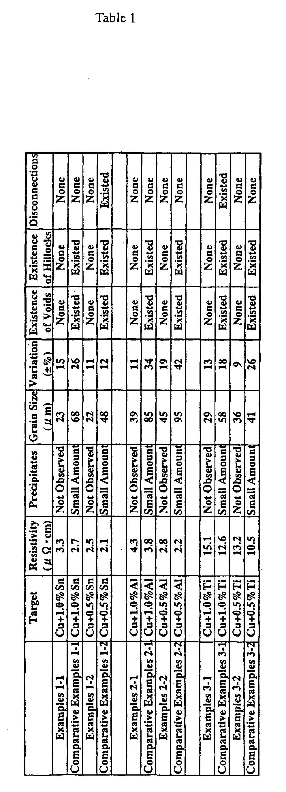
- the crystal grain size was calculated with the method of section prescribed in JIS H0501, and the variation was calculated by radially measuring 17 points (center, and 8 points of 1/2R and 8 points of R) of the sputtering face of the target. Moreover, the existence of precipitates was searched with high resolution SEM.
- the resistivity was calculated by measuring 17 points, respectively, in the upper face, lower face and middle face of the target with the four-terminal method.
- EM characteristics evaluation after depositing a Ta/TaN diffusion barrier to a wiring groove having a wiring width of 0.2 ⁇ m and depth of 0.8 ⁇ m, a copper alloy seed film of 500 ⁇ (deposition film thickness on a flat substrate) was formed on each of the various targets described above. Thereafter, with copper containing phosphorus as the anode, a copper film was embedded with the electroplating method, and excess film at the upper part was removed with the CMP method.
- annealing was performed at 400°C in an Ar gas atmosphere, current having a current density of 10 12 /ampere was applied to the wiring net for 1 hour in order to observe the existence of voids and hillocks in the wiring as electromigration (EM) characteristics.
- EM electromigration
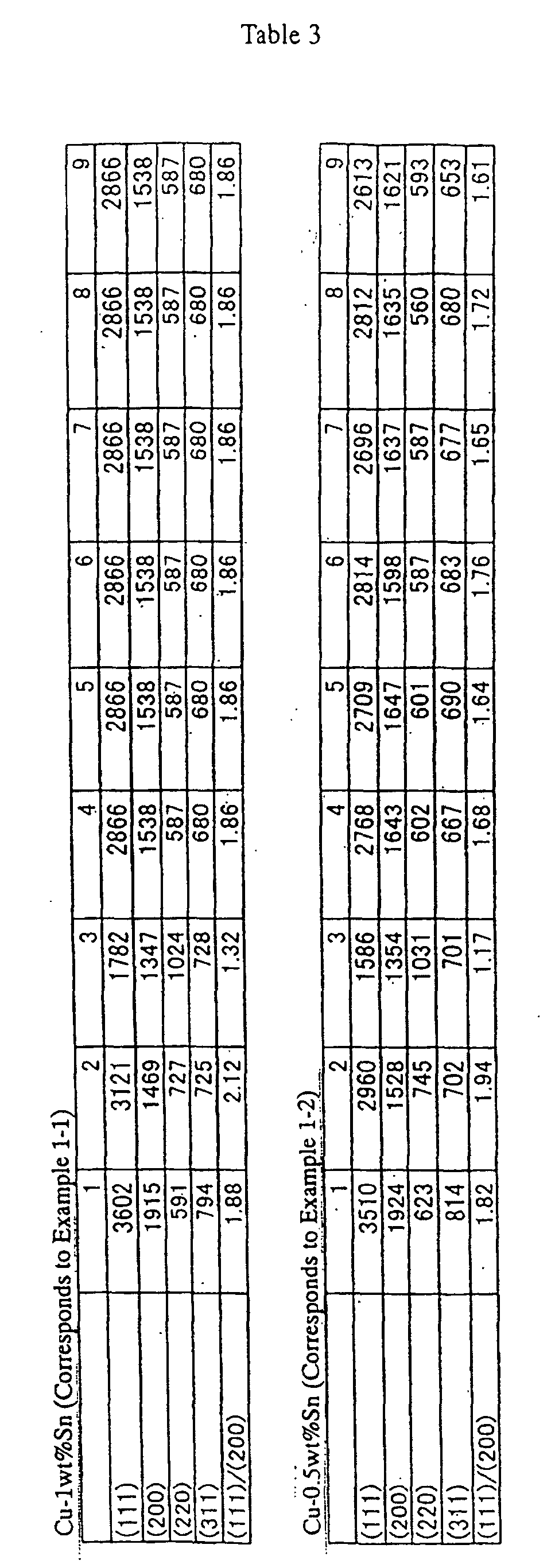
- the ratio I(111)/I(200) of the X-ray diffraction peak intensity I(111) of the (111) face and the X-ray diffraction peak intensity I (200) of the (200) face which corresponds to Example 1-1 and Example 1-2 is shown in Table 3, the ratio of I(111)/I(200) corresponding to Example 2-1 and Example 2-2 is shown in Table 4, and the ratio of I(111)/I(200) corresponding to Examples 3-1 and Example 3-2 is shown in Table 5, respectively.
- Comparative Examples 1-1 to 3-4 are also shown. Comparative Examples 2-3 and 2-4 are targets in which the final heat treatment was not performed, and Comparative Examples 1-3, 1-4, 3-3 and 3-4 are cases where the heat treatment temperature was set to 750°C for 1 hour.
- the copper alloy sputtering target of the present invention possesses favorable characteristics.
- the copper alloy sputtering target of the present invention yields superior effects in that it is capable of preventing the generation of defects such as voids, hillocks and disconnections during copper electroplating, it has low resistivity, it has electromigration resistance and oxidization resistance characteristics, and it is able to form a stable and even seed layer.
Landscapes
- Chemical & Material Sciences (AREA)
- Engineering & Computer Science (AREA)
- Materials Engineering (AREA)
- Mechanical Engineering (AREA)
- Metallurgy (AREA)
- Organic Chemistry (AREA)
- Chemical Kinetics & Catalysis (AREA)
- Physics & Mathematics (AREA)
- Thermal Sciences (AREA)
- Crystallography & Structural Chemistry (AREA)
- Physical Vapour Deposition (AREA)
- Electrodes Of Semiconductors (AREA)
Abstract
Description


Claims (15)
- A copper alloy sputtering target most suitable for formation of an interconnection material of a semiconductor device, particularly for formation of a seed layer, wherein said target contains 0.4 to 5wt% of Sn, the structure of the target does not substantially contain any precipitates, and the resistivity of the target material is 2.3µ Ω cm or more.
- A copper alloy sputtering target according to claim 1, wherein said target contains 0.5 to 1wt% of Sn.
- A copper alloy sputtering target most suitable for formation of an interconnection material of a semiconductor device, particularly for formation of a seed layer, wherein said target contains 0.2 to 5wt% of Al, the structure of the target does not substantially contain any precipitates, and the resistivity of the target material is 2.2µ Ω cm or more.
- A copper alloy sputtering target according to claim 3, wherein said target contains 0.5 to 1wt% of Al.
- A copper alloy sputtering target most suitable for formation of an interconnection material of a semiconductor device, particularly for formation of a seed layer, wherein said target contains 0.3 to 5wt% of Ti, the structure of the target does not substantially contain any precipitates, and the resistivity of the target material is 9µ Ω cm or more.
- A copper alloy sputtering target according to claim 5, wherein said target contains 0.5 to 1wt% of Ti.
- A copper alloy sputtering target most suitable for formation of an interconnection material of a semiconductor device, particularly for formation of a seed layer, wherein said target contains a total of 0.2 to 5wt% of at least one component selected from Sn, Al and Ti, the structure of the target does not substantially contain any precipitates, and the resistivity of the target material is greater than the resistivity of the copper alloy having the same composition in a thermal equilibrium state.
- A copper alloy sputtering target according to claim 7, wherein said target contains a total of 0.5 to 1wt% of at least one component selected from Sn, Al and Ti.
- A copper alloy sputtering target according to claim 7 or claim 8, wherein the increase in resistivity due to the alloying element is resistivity that is 1.2 times or more than that of the thermal equilibrium.
- A copper alloy sputtering target according to any one of claims 1 to 9, wherein Na and K are respectively 0.5ppm or less; Fe, Ni, Cr and Ca are respectively 2ppm or less; U and Th are respectively 1ppb or less, oxygen is 5ppm or less, hydrogen is 2ppm or less; and unavoidable impurities excluding alloying additional elements are 50ppm or less.
- A copper alloy sputtering target according to any one of claims 1 to 9, wherein Na and K are respectively 0.1ppm or less; Fe, Ni, Cr and Ca are respectively 1ppm or less; U and Th are respectively 1ppb or less, oxygen is 5ppm or less, hydrogen is 2ppm or less; and unavoidable impurities excluding alloying additional elements are 10ppm or less.
- A copper alloy sputtering target according to any one of claims 1 to 11, wherein the crystal grain size of the target material is 50µm or less, and the variation in the average grain size by location is within ±20%.
- A copper alloy sputtering target according to any one of claims 1 to 12, wherein the variation in the alloying element of the target material is within 0.2%.
- A copper alloy sputtering target according to any one of claims 1 to 13, wherein, when the alloy contains Al, the ratio I(111)/I(200) of the X-ray diffraction peak intensity I(111) of the (111) face and the X-ray diffraction peak intensity I (200) of the (200) face is 2.2 or more in the sputtering face, and, when the alloy contains Sn and/or Ti, the ratio I(111)/I(200) of the X-ray diffraction peak intensity I(111) of the (111) face and the X-ray diffraction peak intensity I (200) of the (200) face is 2.2 or less in the sputtering face, and the variation in I(111)/I(200) in the sputtering face is respectively within ±30%.
- A manufacturing method of a copper alloy sputtering target according to any one of claims 1 to 14, comprising the steps of performing hot forging and/or hot rolling to a high purity copper alloy ingot obtained by vacuum melting; further performing cold rolling thereto; and thereafter sandwiching this with copper plates underwater and performing forced cooling thereto during heat treatment.
Priority Applications (1)
| Application Number | Priority Date | Filing Date | Title |
|---|---|---|---|
| EP12155232.7A EP2465969B1 (en) | 2002-01-30 | 2002-12-04 | Copper alloy sputtering target |
Applications Claiming Priority (3)
| Application Number | Priority Date | Filing Date | Title |
|---|---|---|---|
| JP2002020928 | 2002-01-30 | ||
| JP2002020928 | 2002-01-30 | ||
| PCT/JP2002/012697 WO2003064722A1 (en) | 2002-01-30 | 2002-12-04 | Copper alloy sputtering target and method for manufacturing the target |
Related Child Applications (2)
| Application Number | Title | Priority Date | Filing Date |
|---|---|---|---|
| EP12155232.7A Division EP2465969B1 (en) | 2002-01-30 | 2002-12-04 | Copper alloy sputtering target |
| EP12155232.7 Division-Into | 2012-02-13 |
Publications (3)
| Publication Number | Publication Date |
|---|---|
| EP1471164A1 true EP1471164A1 (en) | 2004-10-27 |
| EP1471164A4 EP1471164A4 (en) | 2008-04-09 |
| EP1471164B1 EP1471164B1 (en) | 2013-01-23 |
Family
ID=27654375
Family Applications (2)
| Application Number | Title | Priority Date | Filing Date |
|---|---|---|---|
| EP12155232.7A Expired - Lifetime EP2465969B1 (en) | 2002-01-30 | 2002-12-04 | Copper alloy sputtering target |
| EP02783764A Expired - Lifetime EP1471164B1 (en) | 2002-01-30 | 2002-12-04 | Copper alloy sputtering target and method for manufacturing the target |
Family Applications Before (1)
| Application Number | Title | Priority Date | Filing Date |
|---|---|---|---|
| EP12155232.7A Expired - Lifetime EP2465969B1 (en) | 2002-01-30 | 2002-12-04 | Copper alloy sputtering target |
Country Status (6)
| Country | Link |
|---|---|
| US (1) | US9896745B2 (en) |
| EP (2) | EP2465969B1 (en) |
| JP (1) | JP4118814B2 (en) |
| KR (1) | KR100600975B1 (en) |
| TW (1) | TW573035B (en) |
| WO (1) | WO2003064722A1 (en) |
Cited By (4)
| Publication number | Priority date | Publication date | Assignee | Title |
|---|---|---|---|---|
| WO2006005095A1 (en) * | 2004-07-15 | 2006-01-19 | Plansee Se | Material for conductor tracks made of copper alloy |
| EP1584706A4 (en) * | 2002-11-21 | 2008-08-27 | Nippon Mining Co | COPPER ALLOY SPRAY TARGET AND WIRING FOR SEMICONDUCTOR ELEMENT |
| CN102165093A (en) * | 2008-09-30 | 2011-08-24 | Jx日矿日石金属株式会社 | High-purity copper or high-purity copper alloy sputtering target, process for manufacturing the sputtering target, and high-purity copper or high-purity copper alloy sputtered film |
| CN103966558A (en) * | 2013-01-29 | 2014-08-06 | 株式会社Sh铜业 | Cu-Mn alloy sputtering target material, Cu-Mn alloy sputtering target material manufacture method and semiconductor element |
Families Citing this family (36)
| Publication number | Priority date | Publication date | Assignee | Title |
|---|---|---|---|---|
| JPH09267644A (en) * | 1996-01-30 | 1997-10-14 | Hara Kunihito | Awning sheet for vehicle glass |
| KR100700885B1 (en) * | 2003-03-17 | 2007-03-29 | 닛코킨조쿠 가부시키가이샤 | Copper alloy sputtering target, manufacturing method and semiconductor device wiring |
| JP4329532B2 (en) * | 2003-07-15 | 2009-09-09 | 日立電線株式会社 | Flat conductor, method for manufacturing the same, and lead wire |
| EP2626444A3 (en) * | 2003-12-25 | 2013-10-16 | JX Nippon Mining & Metals Corporation | Copper or copper alloy target/copper alloy backing plate assembly |
| JP4524471B2 (en) * | 2004-08-30 | 2010-08-18 | Dowaメタルテック株式会社 | Copper alloy foil and manufacturing method thereof |
| JP5084106B2 (en) * | 2005-03-07 | 2012-11-28 | Dowaメタニクス株式会社 | Copper titanium alloy sheet and method for producing the same |
| JP5263525B2 (en) * | 2006-06-23 | 2013-08-14 | 日本碍子株式会社 | Method for producing copper-based rolled alloy |
| JP2010502841A (en) * | 2006-09-08 | 2010-01-28 | トーソー エスエムディー,インク. | Copper sputtering target having very small crystal grain size and high electromigration resistance and method for producing the same |
| EP2014787B1 (en) * | 2006-10-03 | 2017-09-06 | JX Nippon Mining & Metals Corporation | Cu-Mn ALLOY SPUTTERING TARGET |
| JP4709238B2 (en) * | 2008-02-08 | 2011-06-22 | 株式会社日立製作所 | Cu-based wiring material and electronic component using the same |
| JP5092939B2 (en) * | 2008-07-01 | 2012-12-05 | 日立電線株式会社 | Flat plate copper sputtering target material for TFT and sputtering method |
| JP2010065317A (en) * | 2008-08-14 | 2010-03-25 | Kobe Steel Ltd | DISPLAY DEVICE, AND Cu ALLOY FILM FOR USE IN THE DISPLAY DEVICE |
| JP4620185B2 (en) | 2008-09-30 | 2011-01-26 | Jx日鉱日石金属株式会社 | High purity copper and method for producing high purity copper by electrolysis |
| JP5118618B2 (en) * | 2008-12-24 | 2013-01-16 | Jx日鉱日石金属株式会社 | High purity shape memory alloy target and alloy thin film |
| JPWO2011001974A1 (en) * | 2009-07-01 | 2012-12-13 | Jx日鉱日石金属株式会社 | Cu-Ga target and manufacturing method thereof |
| JP5202643B2 (en) * | 2009-07-23 | 2013-06-05 | Jx日鉱日石金属株式会社 | Cu-Ga alloy sintered compact sputtering target and method for manufacturing the same |
| CN102046836B (en) * | 2009-07-27 | 2012-10-03 | Jx日矿日石金属株式会社 | Cu-Ga sintered sputtering target and method for manufacturing same |
| US8345471B2 (en) | 2010-10-07 | 2013-01-01 | Hynix Semiconductor Inc. | Magneto-resistance element and semiconductor memory device including the same |
| EP2682499A4 (en) * | 2011-03-01 | 2014-09-03 | Jx Nippon Mining & Metals Corp | CATHODE COPPER-TITANIUM ALLOY SPUTTER TARGET, SEMICONDUCTOR WIRING LINE FORMED USING THE CATHODIC SPUTTER TARGET, AND SEMICONDUCTOR ELEMENT AND DEVICE EQUIPPED WITH EACH OF THE SEMICONDUCTOR WIRING LINE |
| US9090970B2 (en) | 2011-09-14 | 2015-07-28 | Jx Nippon Mining & Metals Corporation | High-purity copper-manganese-alloy sputtering target |
| EP2808419B1 (en) | 2012-01-23 | 2016-08-31 | JX Nippon Mining & Metals Corporation | High-purity copper-manganese alloy sputtering target |
| WO2013111689A1 (en) | 2012-01-25 | 2013-08-01 | Jx日鉱日石金属株式会社 | High-purity copper-chromium alloy sputtering target |
| JP5567042B2 (en) * | 2012-02-10 | 2014-08-06 | 株式会社Shカッパープロダクツ | Copper sputtering target material for TFT |
| JP6182296B2 (en) * | 2012-03-09 | 2017-08-16 | 古河電気工業株式会社 | Sputtering target and manufacturing method thereof |
| TWI582254B (en) * | 2012-03-09 | 2017-05-11 | Furukawa Electric Co Ltd | Sputtering target |
| JP6077102B2 (en) * | 2013-03-06 | 2017-02-08 | Jx金属株式会社 | Titanium target for sputtering and manufacturing method thereof |
| WO2015099119A1 (en) * | 2013-12-27 | 2015-07-02 | Jx日鉱日石金属株式会社 | High-purity copper or copper alloy sputtering target, and method for producing same |
| WO2015151901A1 (en) * | 2014-03-31 | 2015-10-08 | Jx日鉱日石金属株式会社 | Copper or copper alloy sputtering target |
| JP6358340B2 (en) * | 2014-12-12 | 2018-07-18 | 新日鐵住金株式会社 | Oriented copper plate, copper-clad laminate, flexible circuit board, and electronic device |
| KR20170118586A (en) * | 2015-02-19 | 2017-10-25 | 미쓰이금속광업주식회사 | Sputtering target of copper-based alloy |
| US10494712B2 (en) | 2015-05-21 | 2019-12-03 | Jx Nippon Mining & Metals Corporation | Copper alloy sputtering target and method for manufacturing same |
| JP6567762B2 (en) * | 2016-03-09 | 2019-08-28 | Jx金属株式会社 | Copper and copper alloy targets containing argon or hydrogen |
| KR102680283B1 (en) * | 2016-08-29 | 2024-07-03 | 한국재료연구원 | Copper thin layer substrate and fabrication method for the same |
| TWI663274B (en) | 2017-03-30 | 2019-06-21 | 日商Jx金屬股份有限公司 | Sputtering target and manufacturing method thereof |
| US10400700B2 (en) * | 2017-06-01 | 2019-09-03 | Caterpillar Inc. | Segmented calibration for aftertreatment optimization in internal combustion engine system |
| JP6650987B1 (en) * | 2018-11-09 | 2020-02-19 | Jx金属株式会社 | Titanium copper foil, brass products, electronic equipment parts and autofocus camera modules |
Family Cites Families (28)
| Publication number | Priority date | Publication date | Assignee | Title |
|---|---|---|---|---|
| JPS4923127A (en) | 1972-06-26 | 1974-03-01 | ||
| JPS61231131A (en) | 1985-04-05 | 1986-10-15 | Kobe Steel Ltd | Corrosion resistant copper alloy pipe |
| FR2583735B1 (en) | 1985-06-20 | 1990-11-23 | Rhone Poulenc Spec Chim | NEW COLLOIDAL DISPERSIONS OF A CERIUM IV COMPOUND IN AQUEOUS MEDIA AND THEIR PROCESS FOR OBTAINING SAME. |
| US4822560A (en) * | 1985-10-10 | 1989-04-18 | The Furukawa Electric Co., Ltd. | Copper alloy and method of manufacturing the same |
| JPH0653901B2 (en) | 1986-09-08 | 1994-07-20 | 古河電気工業株式会社 | Copper alloy for electronic and electrical equipment |
| DE3784605T2 (en) * | 1986-09-17 | 1993-06-17 | Fujitsu Ltd | METHOD FOR PRODUCING A SEMICONDUCTOR DEVICE AND SEMICONDUCTOR DEVICE. |
| JP2511289B2 (en) * | 1988-03-30 | 1996-06-26 | 株式会社日立製作所 | Semiconductor device |
| JP2552920B2 (en) | 1989-08-11 | 1996-11-13 | 住友金属鉱山株式会社 | Copper alloy for backing plate |
| JP2862727B2 (en) | 1992-05-12 | 1999-03-03 | 同和鉱業株式会社 | Sputtering target for forming metal thin film and method for producing the same |
| JPH06177128A (en) * | 1992-12-07 | 1994-06-24 | Japan Energy Corp | Semiconductor device and manufacturing method thereof |
| EP0601509A1 (en) * | 1992-12-07 | 1994-06-15 | Nikko Kyodo Co., Ltd. | Semiconductor devices and method of manufacturing the same |
| DE19525330C2 (en) * | 1995-07-12 | 1998-07-09 | Glyco Metall Werke | Layer material |
| JP3819487B2 (en) | 1996-08-16 | 2006-09-06 | 同和鉱業株式会社 | Manufacturing method of semiconductor device |
| JP3403918B2 (en) * | 1997-06-02 | 2003-05-06 | 株式会社ジャパンエナジー | High purity copper sputtering target and thin film |
| JPH10330927A (en) | 1997-06-05 | 1998-12-15 | Riyouka Massey Kk | Sputtering target material made of aluminum alloy |
| US6569270B2 (en) * | 1997-07-11 | 2003-05-27 | Honeywell International Inc. | Process for producing a metal article |
| JP2000034562A (en) | 1998-07-14 | 2000-02-02 | Japan Energy Corp | Sputtering target and thin film forming equipment parts |
| JP2000087158A (en) | 1998-09-11 | 2000-03-28 | Furukawa Electric Co Ltd:The | Copper alloy for semiconductor lead frame |
| JP2000239836A (en) | 1999-02-23 | 2000-09-05 | Japan Energy Corp | High purity copper or copper alloy sputtering target and method for producing the same |
| US6113761A (en) * | 1999-06-02 | 2000-09-05 | Johnson Matthey Electronics, Inc. | Copper sputtering target assembly and method of making same |
| US6391163B1 (en) * | 1999-09-27 | 2002-05-21 | Applied Materials, Inc. | Method of enhancing hardness of sputter deposited copper films |
| JP4005295B2 (en) | 2000-03-31 | 2007-11-07 | 富士通株式会社 | Manufacturing method of semiconductor device |
| US6228759B1 (en) * | 2000-05-02 | 2001-05-08 | Advanced Micro Devices, Inc. | Method of forming an alloy precipitate to surround interconnect to minimize electromigration |
| JP2002075995A (en) * | 2000-08-24 | 2002-03-15 | Matsushita Electric Ind Co Ltd | Semiconductor device and manufacturing method thereof |
| JP4794802B2 (en) * | 2002-11-21 | 2011-10-19 | Jx日鉱日石金属株式会社 | Copper alloy sputtering target and semiconductor device wiring |
| KR100700885B1 (en) * | 2003-03-17 | 2007-03-29 | 닛코킨조쿠 가부시키가이샤 | Copper alloy sputtering target, manufacturing method and semiconductor device wiring |
| EP2626444A3 (en) * | 2003-12-25 | 2013-10-16 | JX Nippon Mining & Metals Corporation | Copper or copper alloy target/copper alloy backing plate assembly |
| EP1785505B1 (en) * | 2004-08-10 | 2009-09-02 | Nippon Mining & Metals Co., Ltd. | Barrier film for flexible copper substrate and sputtering target for forming barrier film |
-
2002
- 2002-12-04 US US10/501,117 patent/US9896745B2/en active Active
- 2002-12-04 EP EP12155232.7A patent/EP2465969B1/en not_active Expired - Lifetime
- 2002-12-04 WO PCT/JP2002/012697 patent/WO2003064722A1/en not_active Ceased
- 2002-12-04 KR KR1020047011298A patent/KR100600975B1/en not_active Expired - Lifetime
- 2002-12-04 JP JP2003564309A patent/JP4118814B2/en not_active Expired - Lifetime
- 2002-12-04 EP EP02783764A patent/EP1471164B1/en not_active Expired - Lifetime
- 2002-12-09 TW TW091135520A patent/TW573035B/en not_active IP Right Cessation
Cited By (6)
| Publication number | Priority date | Publication date | Assignee | Title |
|---|---|---|---|---|
| EP1584706A4 (en) * | 2002-11-21 | 2008-08-27 | Nippon Mining Co | COPPER ALLOY SPRAY TARGET AND WIRING FOR SEMICONDUCTOR ELEMENT |
| EP2309021A1 (en) * | 2002-11-21 | 2011-04-13 | Nippon Mining & Metals Co., Ltd. | Copper alloy sputtering target and semiconductor element wiring |
| WO2006005095A1 (en) * | 2004-07-15 | 2006-01-19 | Plansee Se | Material for conductor tracks made of copper alloy |
| CN102165093A (en) * | 2008-09-30 | 2011-08-24 | Jx日矿日石金属株式会社 | High-purity copper or high-purity copper alloy sputtering target, process for manufacturing the sputtering target, and high-purity copper or high-purity copper alloy sputtered film |
| CN103966558A (en) * | 2013-01-29 | 2014-08-06 | 株式会社Sh铜业 | Cu-Mn alloy sputtering target material, Cu-Mn alloy sputtering target material manufacture method and semiconductor element |
| CN103966558B (en) * | 2013-01-29 | 2017-08-04 | 株式会社Sh铜业 | Cu Mn alloy sputtering targets, the manufacture method of Cu Mn alloy sputtering targets and semiconductor element |
Also Published As
| Publication number | Publication date |
|---|---|
| US9896745B2 (en) | 2018-02-20 |
| KR100600975B1 (en) | 2006-07-13 |
| EP2465969A2 (en) | 2012-06-20 |
| JP4118814B2 (en) | 2008-07-16 |
| WO2003064722A1 (en) | 2003-08-07 |
| EP1471164B1 (en) | 2013-01-23 |
| EP2465969B1 (en) | 2016-05-11 |
| EP1471164A4 (en) | 2008-04-09 |
| EP2465969A3 (en) | 2013-07-17 |
| JPWO2003064722A1 (en) | 2005-05-26 |
| TW200302287A (en) | 2003-08-01 |
| US20050121320A1 (en) | 2005-06-09 |
| KR20040078673A (en) | 2004-09-10 |
| TW573035B (en) | 2004-01-21 |
Similar Documents
| Publication | Publication Date | Title |
|---|---|---|
| US9896745B2 (en) | Copper alloy sputtering target and method for manufacturing the target | |
| US10665462B2 (en) | Copper alloy sputtering target and semiconductor element wiring | |
| TWI248468B (en) | Copper alloy sputtering target, process for producing the same and semiconductor element wiring | |
| US20100013096A1 (en) | Cu-Mn Alloy Sputtering Target and Semiconductor Wiring | |
| CN101395296B (en) | Sputtering target | |
| JPH10330923A (en) | High purity copper sputtering target and thin film | |
| US10431439B2 (en) | Tantalum sputtering target | |
| US10494712B2 (en) | Copper alloy sputtering target and method for manufacturing same | |
| TW201241216A (en) | Copper-titanium alloy sputtering target, semiconductor wiring line formed using the sputtering target, and semiconductor element and device each equipped with the semiconductor wiring line | |
| JP2009114539A (en) | Copper alloy sputtering target and semiconductor device wiring | |
| JP2000034562A (en) | Sputtering target and thin film forming equipment parts | |
| JP6961861B1 (en) | Copper alloy strips and their manufacturing methods, resistor materials for resistors using them, and resistors | |
| TW202200800A (en) | Copper alloy strip and its manufacturing method, resistance material for resistor using the copper alloy strip and resistor | |
| EP0299605B1 (en) | Iron-copper-chromium alloy for high-strength lead frame or pin grid array and process for preparation thereof | |
| US9909196B2 (en) | High-purity copper-cobalt alloy sputtering target | |
| JP2023097756A (en) | Copper alloys, copper alloy plastic processed materials, parts for electronic and electrical equipment, terminals, bus bars, lead frames, heat dissipation substrates | |
| US20040123920A1 (en) | Homogenous solid solution alloys for sputter-deposited thin films |
Legal Events
| Date | Code | Title | Description |
|---|---|---|---|
| PUAI | Public reference made under article 153(3) epc to a published international application that has entered the european phase |
Free format text: ORIGINAL CODE: 0009012 |
|
| 17P | Request for examination filed |
Effective date: 20040709 |
|
| AK | Designated contracting states |
Kind code of ref document: A1 Designated state(s): AT BE BG CH CY CZ DE DK EE ES FI FR GB GR IE IT LI LU MC NL PT SE SI SK TR |
|
| RAP1 | Party data changed (applicant data changed or rights of an application transferred) |
Owner name: NIKKO MATERIALS CO., LTD. |
|
| RAP1 | Party data changed (applicant data changed or rights of an application transferred) |
Owner name: NIPPON MINING & METALS CO., LTD. |
|
| A4 | Supplementary search report drawn up and despatched |
Effective date: 20080306 |
|
| 17Q | First examination report despatched |
Effective date: 20100216 |
|
| RAP1 | Party data changed (applicant data changed or rights of an application transferred) |
Owner name: JX NIPPON MINING & METALS CORPORATION |
|
| RIC1 | Information provided on ipc code assigned before grant |
Ipc: C22F 1/00 20060101ALI20120808BHEP Ipc: H01L 21/768 20060101ALI20120808BHEP Ipc: C23C 14/34 20060101AFI20120808BHEP Ipc: C22C 19/00 20060101ALI20120808BHEP Ipc: C22C 9/02 20060101ALI20120808BHEP Ipc: C22C 9/01 20060101ALI20120808BHEP Ipc: C22C 9/00 20060101ALI20120808BHEP |
|
| GRAP | Despatch of communication of intention to grant a patent |
Free format text: ORIGINAL CODE: EPIDOSNIGR1 |
|
| GRAS | Grant fee paid |
Free format text: ORIGINAL CODE: EPIDOSNIGR3 |
|
| GRAA | (expected) grant |
Free format text: ORIGINAL CODE: 0009210 |
|
| AK | Designated contracting states |
Kind code of ref document: B1 Designated state(s): DE FR IT |
|
| REG | Reference to a national code |
Ref country code: DE Ref legal event code: R096 Ref document number: 60244459 Country of ref document: DE Effective date: 20130321 |
|
| PLBE | No opposition filed within time limit |
Free format text: ORIGINAL CODE: 0009261 |
|
| STAA | Information on the status of an ep patent application or granted ep patent |
Free format text: STATUS: NO OPPOSITION FILED WITHIN TIME LIMIT |
|
| 26N | No opposition filed |
Effective date: 20131024 |
|
| REG | Reference to a national code |
Ref country code: DE Ref legal event code: R097 Ref document number: 60244459 Country of ref document: DE Effective date: 20131024 |
|
| REG | Reference to a national code |
Ref country code: FR Ref legal event code: PLFP Year of fee payment: 14 |
|
| REG | Reference to a national code |
Ref country code: FR Ref legal event code: PLFP Year of fee payment: 15 |
|
| REG | Reference to a national code |
Ref country code: FR Ref legal event code: CA Effective date: 20170801 |
|
| REG | Reference to a national code |
Ref country code: FR Ref legal event code: PLFP Year of fee payment: 16 |
|
| PGFP | Annual fee paid to national office [announced via postgrant information from national office to epo] |
Ref country code: FR Payment date: 20211109 Year of fee payment: 20 Ref country code: DE Payment date: 20211102 Year of fee payment: 20 |
|
| PGFP | Annual fee paid to national office [announced via postgrant information from national office to epo] |
Ref country code: IT Payment date: 20211110 Year of fee payment: 20 |
|
| REG | Reference to a national code |
Ref country code: DE Ref legal event code: R071 Ref document number: 60244459 Country of ref document: DE |