EP1469345A2 - Methode zur Bestimmung von Regeln zur Aufteilung in komplementäre Muster, Methode zur Aufteilung in komplementäre Muster, sowie Programm dafür - Google Patents
Methode zur Bestimmung von Regeln zur Aufteilung in komplementäre Muster, Methode zur Aufteilung in komplementäre Muster, sowie Programm dafür Download PDFInfo
- Publication number
- EP1469345A2 EP1469345A2 EP04291022A EP04291022A EP1469345A2 EP 1469345 A2 EP1469345 A2 EP 1469345A2 EP 04291022 A EP04291022 A EP 04291022A EP 04291022 A EP04291022 A EP 04291022A EP 1469345 A2 EP1469345 A2 EP 1469345A2
- Authority
- EP
- European Patent Office
- Prior art keywords
- pattern
- division
- analysis
- mask
- displacement
- Prior art date
- Legal status (The legal status is an assumption and is not a legal conclusion. Google has not performed a legal analysis and makes no representation as to the accuracy of the status listed.)
- Granted
Links
Images







Classifications
-
- G—PHYSICS
- G03—PHOTOGRAPHY; CINEMATOGRAPHY; ANALOGOUS TECHNIQUES USING WAVES OTHER THAN OPTICAL WAVES; ELECTROGRAPHY; HOLOGRAPHY
- G03F—PHOTOMECHANICAL PRODUCTION OF TEXTURED OR PATTERNED SURFACES, e.g. FOR PRINTING, FOR PROCESSING OF SEMICONDUCTOR DEVICES; MATERIALS THEREFOR; ORIGINALS THEREFOR; APPARATUS SPECIALLY ADAPTED THEREFOR
- G03F7/00—Photomechanical, e.g. photolithographic, production of textured or patterned surfaces, e.g. printing surfaces; Materials therefor, e.g. comprising photoresists; Apparatus specially adapted therefor
- G03F7/20—Exposure; Apparatus therefor
- G03F7/2045—Exposure; Apparatus therefor using originals with apertures, e.g. stencil exposure masks
- G03F7/2047—Exposure with radiation other than visible light or UV light, e.g. shadow printing, proximity printing
-
- G—PHYSICS
- G03—PHOTOGRAPHY; CINEMATOGRAPHY; ANALOGOUS TECHNIQUES USING WAVES OTHER THAN OPTICAL WAVES; ELECTROGRAPHY; HOLOGRAPHY
- G03F—PHOTOMECHANICAL PRODUCTION OF TEXTURED OR PATTERNED SURFACES, e.g. FOR PRINTING, FOR PROCESSING OF SEMICONDUCTOR DEVICES; MATERIALS THEREFOR; ORIGINALS THEREFOR; APPARATUS SPECIALLY ADAPTED THEREFOR
- G03F1/00—Originals for photomechanical production of textured or patterned surfaces, e.g., masks, photo-masks, reticles; Mask blanks or pellicles therefor; Containers specially adapted therefor; Preparation thereof
- G03F1/20—Masks or mask blanks for imaging by charged particle beam [CPB] radiation, e.g. by electron beam; Preparation thereof
-
- H—ELECTRICITY
- H01—ELECTRIC ELEMENTS
- H01J—ELECTRIC DISCHARGE TUBES OR DISCHARGE LAMPS
- H01J37/00—Discharge tubes with provision for introducing objects or material to be exposed to the discharge, e.g. for the purpose of examination or processing thereof
- H01J37/30—Electron-beam or ion-beam tubes for localised treatment of objects
- H01J37/317—Electron-beam or ion-beam tubes for localised treatment of objects for changing properties of the objects or for applying thin layers thereon, e.g. for ion implantation
- H01J37/3174—Particle-beam lithography, e.g. electron beam lithography
-
- H—ELECTRICITY
- H01—ELECTRIC ELEMENTS
- H01J—ELECTRIC DISCHARGE TUBES OR DISCHARGE LAMPS
- H01J2237/00—Discharge tubes exposing object to beam, e.g. for analysis treatment, etching, imaging
- H01J2237/30—Electron or ion beam tubes for processing objects
- H01J2237/317—Processing objects on a microscale
- H01J2237/3175—Lithography
- H01J2237/31793—Problems associated with lithography
- H01J2237/31794—Problems associated with lithography affecting masks
Definitions
- the present invention relates to a method of determining conditions for complementary division of a pattern comprised by an opening formed in a stencil mask used in for example a lithography step of a semiconductor device and a complementary division method and a program using the same.
- X-ray, ion, electron beam lithography use stencil masks. Patterns are formed in a stencil mask by openings, so donut-shaped and other hard-to-form patterns are formed by complementary division (see Japanese Patent No. 3348097, Japanese Unexamined Patent Publication (Kokai) No. 2003-45786, Japanese Unexamined Patent Publication (Kokai) No. 2002-353102, Japanese Unexamined Patent Publication (Kokai) No. 2002-260983, and Japanese Unexamined Patent Publication (Kokai) No. 2002-260992).
- Stencil masks suffer from two problems. One is that an internal stress changes by the formation of an opening of a pattern in the membrane (thin film) and therefore the positions of the surrounding patterns change. Another is that there is a possibility of mask destruction due to the concentration of stress occurring due to the opening shape. The occurrence of this problem can be reduced by complementary division.
- the complementary division has been mainly performed for hard-to-form pattterns, for example, donut patterns and leaf patterns.
- the optimum complementary division conditions have not been proposed for other patterns such as line patterns, line-and-space patterns (LS patterns), and large area patterns which become factors causing pattern displacement and mask destruction due to stress concentration.
- An object of the present invention is to provide a complementary division condition determining method and program able to propose the optimum complementary division conditions for suppression of pattern displacement and mask destruction.
- Another object of the present invention is to provide a complementary division method for performing complementary division processing by using the above optimum complementary division conditions.
- a complementary division condition determining method comprising a step of measuring a displacement of a peripheral mark when forming an opening in a mask and determining an internal stress of said mask based on said measured displacement; a first analysis step of setting a first analysis model forming split patterns obtained by dividing a pattern for division under various division conditions at said mask having said internal stress and analyzing pattern displacement and stress concentration occurring due to the openings of said split patterns based on said first analysis model; a second analysis step of setting a second analysis model assuming a membrane between said split patterns as a two-ended fixed structure and analyzing the displacement of the membrane between said split patterns due to the external force based on said second analysis model; and a step of determining complementary division conditions based on the results of said first and second analysis steps and an allowable displacement and stress concentration.
- a program for making a computer execute processing for determining division conditions for dividing pattern data comprising a routine for determining an internal stress of a mask based on a displacement of a peripheral mark when forming an opening in the mask; a first analysis routine for setting a first analysis model forming split patterns obtained by dividing a pattern for division under various division conditions at said mask having said internal stress and analyzing pattern displacement and stress concentration occurring due to the openings of said split patterns based on said first analysis model; a second analysis routine for setting a second analysis model assuming a membrane between said split patterns as a two-ended fixed structure and analyzing the displacement of the membrane between said split patterns due to the external force based on said second analysis model; and a routine for determining the complementary division conditions based on the results in said first and second analysis routines and an allowable displacement and stress concentration.
- a complementary division method for dividing a pattern defining an opening formed in a mask comprising a step of measuring a displacement of a peripheral mark when forming an opening in said mask and determining an internal stress of said mask based on the measured displacement; a first analysis step of setting a first analysis model forming split patterns obtained by dividing a pattern for division under various division conditions at said mask having said internal stress and analyzing pattern displacement and stress concentration occurring due to the openings of said split patterns based on said first analysis model; a second analysis step of setting a second analysis model assuming a membrane between said split patterns as a two-ended fixed structure and analyzing the displacement of the membrane between said split patterns due to external force based on said second analysis model; a step of determining the complementary division conditions based on the results of said first and second analysis steps and an allowable displacement and stress concentration; and a step of extracting said pattern for division from the pattern data of said mask and dividing said pattern for division based on said
- the complementary division condition determining method and program of the present invention determine the internal stress of the mask based on the displacement of a peripheral mark when forming an opening in the mask and use this value for the first analysis.
- the pattern displacement and stress concentration occurring due to the openings of the split patterns are analyzed based on the first analysis model.
- the displacement of the membrane between the split patterns due to external force is analyzed.
- the order of the first and second analyses is not important.
- the complementary division conditions are determined based on the allowable displacement and stress concentration.
- the complementary division method of the present invention divides the pattern for division based on the complementary division conditions determined as described above.
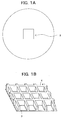
- FIG. 1A is a plan view of a stencil mask prepared when applying the complementary division method according to the present invention
- FIG. 1B is a detailed perspective view in an exposure area of FIG. 1A.
- an exposure area 2 to which X-rays, ions, or electron beams are emitted is arranged at the center of for example a disk-shaped member.
- a plurality of thin films (hereinafter referred to as "membranes") 3 having thicknesses of about 100 nm to 10 ⁇ m are formed in the exposure area 2. Not illustrated opening patterns are formed in the membranes 3.
- struts 4 are formed for reinforcing the thin membranes 3.
- the above stencil mask is prepared based on for example an SOI wafer.
- the thickness of the struts 4 is the same as that of for example an 8-inch diameter silicon substrate, that is, about 725 ⁇ m.
- FIG. 2 is a flow chart of complementary division for arranging patterns comprised by openings in the above stencil mask.
- a pattern is extracted from the pattern data (design data) (step ST1) and judged whether or not the extracted pattern is a hard-to-form pattern such as a donut pattern or a leaf pattern (step ST2).
- a hard-to-form pattern is always complementary divided by the first complementary division processing (step ST3).
- FIGS. 3A to 3F are views for explaining the first complementary division processing.
- the explanation is given with reference to the examples of a donut pattern and leaf pattern which become problems when preparing a stencil mask.
- a donut pattern n1 and a leaf pattern n2 are included in pattern data N as shown in FIG. 3A
- a pattern n211 at the center portion cannot be supported and therefore the shape n21 results.
- a pattern n31 missing the center portion is formed in a wafer W as shown in FIG. 3C.
- the portion supporting the center projecting portion n221 is small, so it droops due to gravity. Stress may concentrate at the support point thereof to cause a destruction.
- this stencil mask M for exposure, for example, as shown in FIG.3C, a pattern n32 having a shape with a deformed center portion n321 is formed.
- the donut pattern n1 is divided into split patterns n1-1 to n1-4.
- the split patterns n1-1 and n1-2 are arranged in a first area M1 of the mask, while the split patterns n1-3 and n1-4 are arranged in a second area M2 of the mask.
- a donut pattern n301 will be formed at the wafer W as shown in FIG. 3F.
- the leaf pattern n2 is divided into split patterns n2-1 to n2-3.
- the split patterns n2-1 and n2-2 are arranged in the first area M1 of the mask, and the split pattern n2-3 is arranged in the second area M2 of the mask. Then, by exposing the areas M1 and M2 of the mask overlappingly, a leaf pattern n302 will be formed in the wafer W as shown in FIG. 3F.
- a pattern not processed by the first complementary division processing or a pattern to which the first complementary division processing was applied is a pattern causing position offset of the other patterns or the mask destruction in the stencil mask. If necessary, it is divided by the second complementary division processing (step ST4).
- the complementary division processing is terminated.
- the complementarily split patterns are formed allocated to the different areas of the mask as explained with reference to FIG. 3E.
- the present invention relates to the second complementary division processing in the flow of the complementary division and provides a complementary division condition determining method for determining the complementary division conditions of a pattern for complementary division in the second complementary division processing and a program for executing this and a complementary division method for performing the complementary division using the determined complementary division conditions.
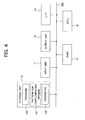
- FIG. 4 is a block diagram of the hardware of a data processing system (computer) for determining complementary division conditions by running the program according to the present invention.
- the data processing device has, as shown in FIG. 4, an input unit 11, an output unit 12, an interface (I/F) 13, a RAM 14, a storage unit 15, and a central processing unit (CPU) 16.
- the input unit 11, the output unit 12, the I/F 13, the RAM 14, the storage unit 15, and the CPU 16 are connected by a bus BS.
- the input unit 11 outputs intended input data to the CPU 16.
- the input unit 11 is a data input device such as a keyboard or mouse, CDROM (R-RW) drive, or floppy disk drive (FD).
- the input unit 11 can be used for input of for example a pattern for complementary division 151 and parameters 152 as the input data.
- the output unit 12 outputs data in accordance with the predetermined output data output from the CPU 16.
- the output unit 12 is a display etc. and performs a display in accordance with the output data output from the CPU 16.
- the interface (I/F) 13 transfers the intended data with another data processing system under the control of the CPU 16.
- the RAM 14 is used as a workspace when the CPU 16 performs the predetermined processing.
- the storage unit 15 is used for writing and reading the intended data by the CPU 16.
- the storage unit 15 stores the pattern for complementary division 151, various parameters 152, etc. in addition to a program 150 according to the present invention.
- the program 150 includes processing routines concerning the complementary division condition determining processing according to the present invention and executed by the CPU 16 using the RAM 14 as a workspace.
- the pattern for complementary division 151 is a pattern for the second complementary division processing as will be explained later.
- the parameters 152 include data of characteristics of the stencil mask (material etc. of the mask) used for the stress-strain analysis, values of the allowable displacement and stress concentration, and numerical values used for judgment in various analyses.
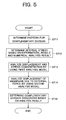
- FIG. 5 is a flow chart of the complementary division condition determining method executed by the above program.
- a pattern for the second complementary division processing is determined (step ST11).
- the processing from step ST12 to step ST15 is performed for the pattern for complementary division to determine the division conditions for the pattern.
- FIGS. 6A to 6D show examples of patterns for second complementary division processing.
- hard-to-form shapes such as donut patterns and leaf patterns are dealt with by the first complementary division processing.
- the second complementary division processing deals with mainly close to rectangular patterns which are not hard to form, but which may cause position offset of other patterns or mask destruction in the stencil mask.
- the patterns shown in FIG. 6A are contact hole patterns for contact to the device.
- the pattern shown in FIG. 6B is a line pattern (including also a general rectangle) long in one direction and without any patterns at its periphery.
- the patterns shown in FIG. 6C are line-and-space patterns (LS patterns) comprised of a plurality of line patterns arranged side by side at predetermined intervals.
- the pattern shown in FIG. 6D is a large area pattern as will be defined later.
- the optimum complementary division conditions for these individual patterns for division are determined by the flow shown in FIG. 5.
- the determined complementary division conditions are used in the second complementary division processing shown in FIG. 2 (step ST4). Due to the optimal division of these patterns in the second complementary division processing, the offset or the stress concentration at each opening is reduced to the lowest limit and thereby the entire offset or stress concentration can be minimized.
- the division conditions of a pattern for complementary division are determned by stress-strain analysis by the finite element method etc., but it is first necessary to determine the conditions used for this stress-strain analysis (step ST12).
- the physical properties of the material of the stencil mask are made, for example, a Young's modulus of 63.9 MPa and a Poisson ratio of 0.2 as disclosed in Jpn. J. Appl. Phys., vol. 38 (1999) pp. 7027-7030.
- the internal stress value of a stencil mask is unknown. Namely, this is because even if the physical properties of the material of stencil masks used are the same, the internal stresses remaining after the fabrication of the stencil masks will differ due to the difference of the process, dimensions, etc. Accordingly, in the present invention, the results of experiments and the results of numerical analysis are calilbrated so as to determine the internal stress of a stencil mask to be prepared (step ST12).
- FIG. 7 is an enlarged view of a pattern of a calibration use mask.
- the displacement of position offset measurement marks 3b arranged at the periphery of an opening 3a of 100 ⁇ m square when forming the opening 3a in for example a membrane 3 of 1 mm square surrounded by not illustrated struts is found by experiment and numerical analysis. Note that the position offset measurement marks 3b are not openings. In the present experiment, use is made of mask blanks of the actually prepared stencil mask.
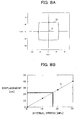
- FIG. 8A shows measurement results of the displacement of position offset measurement marks 3b when actually fabricating a stencil mask having the pattern shown in FIG. 7.
- FIG. 8A shows the result of measurement of the displacement of the position offset measurement marks 3b at eight points located nearest the periphery of the opening 3a and the position offset measurement marks 3b at four points located outside the opening 3a in a horizontal direction.
- FIG. 8A shows a position D1 of the position offset measurement marks 3b from the center O of the opening 3a.
- the displacement of the position offset measurement marks 3b at the periphery was 22 nm from the experimental result shown in FIG. 8A.
- FIG. 8B is a view of a relationship between the internal stress remaining in the stencil mask and the pattern displacement calculated by numerical analysis (simulation) from the values of the physical properties of the material etc. of the stencil mask when forming an opening having the same pattern as that in the experiment. As shown by the line S in the figure, the position offset of a peripheral mark when forming an opening increases in proportion to the internal stress remaining in the stencil mask.
- the internal stress of the stencil mask is found. In the present example, in the previous experimental result, the displacement was 22 nm, therefore, as shown in FIG. 8B, the internal stress existing in the stencil mask becomes 17 MPa.
- step ST12 After determining the internal stress of the stencil mask as described above (step ST12), the displacement and stress concentration occurring due to the pattern comprised by the opening are analyzed by using the first analysis model (step ST13). As the conditions of the analysis at this time, other than the previously determined internal stress, use is made of the Young's modulus and the Poisson ratio. Further, the displacement of the membrane between the patterns due to external force received is analyzed by using the second analysis model (step ST14). Below, a detailed explanation will be given of the processing of steps ST13 and ST14.
- FIG. 9 is a view of the first analysis model for analyzing the position offset and stress concentration occurring due to opening patterns obtained after complementary division formed in a membrane.
- the first analysis model assumes a case of formation of split patterns obtained by dividing a pattern for complementary division under various division conditions in a stencil mask having internal stress found previously.
- FIG. 9 shows a first model in which split patterns SP comprised by openings obtained by complementary division of for example a line-shaped pre-division pattern PP are formed in the membrane 3.
- split patterns SP comprised by openings obtained by complementary division of for example a line-shaped pre-division pattern PP are formed in the membrane 3.
- LY is mainly a short side of the rectangular shaped pattern for division
- LX is a divided width.
- FIG. 10 is a view of a second analysis model for analyzing displacement of the membrane between the split patterns due to external force.
- the second analysis model is a model taking note of the fact that the membrane 3 between the split patterns comprised by the openings has a two-ended fixed structure (refer to FIG. 9).
- the second analysis model is a model taking note of the fact that two ends of the membrane having the width LX and the length LY are fixed.
- step ST15 After the first analysis (step ST13 of FIG. 5) using the first analysis model and the second analysis (step ST14 of FIG. 5) using the second analysis model, the complementary division conditions are determined from these two analysis results and the allowable offset and stress concentration (step ST15).
- the values of the allowable offset and stress concentration are input and stored as parameters 152 in advance (refer to FIG. 4).
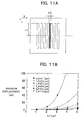
- stress-strain analysis is carried out by for example the finite element method while changing the LX and LY (corresponding to the divided width in the present example) of the second analysis model envisioning the membrane indicated by hatching of the LS patterns shown in FIG. 11A.
- the analyzed result of displacement and the offset allowable by the stencil mask are compared to determine the optimum complementary division widths. For example, as found in the above, the result obtained by stress-strain analysis by setting the external force at 1.461 MPa is shown in FIG. 11B.
- the second analysis model in this case uses the membrane between lines arranged in parallel as in FIG. 11A as a model, so LY becomes a divided width for dividing the LS patterns.
- LX 0.1, 0.2, 0.3, 0.4, 0.5, 1.0
- the allowable maximum displacement is 1/2 of the membrane width LX.
- a divided width of the LS patterns is made 3 ⁇ m or less.
- the divided width in the LS patterns is determined by the second analysis processing.
- Ra and Re are any values different for every stencil mask.
- the divided width (first divided width) of the above equation (2) use is made of the value of the divided width obtained by the determination of the divided width for the line pattern and the LS patterns described above.
- the left side of the above equation (1) is the area ratio between the circumscribed rectangle CP and the pattern BP.
- the above equation (2) is a conditional equation concerning the aspect ratio of patterns after division and is determined depending upon the stencil mask.
- the first analysis processing by the first analysis model (step ST14) and the second analysis processing by the second analysis model (step ST15) are carried out.
- the first analysis model is used for analysis of the displacement and Mises stress in the case of changing the LX and LY of the split patterns comprised by the openings (refer to FIG. 9).
- the second analysis model is used for analysis of the displacement of the membrane portion between the split patterns due to external force.
- FIG. 13A shows the analysis result of the pattern displacement; and
- FIG. 13B shows the analysis result of the Mises stress.
- FIG. 14 shows the result obtained by analyzing the displacement of the membrane due to external force by using the second model taking note of the membrane between the patterns divided under the same conditions as those of FIGS. 13A and 13B.
- the external force 1.641 MPa determined in the previous step.
- the optimum divided width of a large area pattern can be determined.
- a value which does not become larger than the allowable aspect ratio and does not exceed the circumscribed rectangle short side is preferred.
- the pattern displacement and stress concentration generated by the openings of split patterns are analyzed by the first analysis based on the internal stress value of the stencil mask determined based on experiments and simulation (numerical analysis). Further, the displacement of the membrane between the split patterns due to external force is analyzed by the second analysis. By these two analyses, the influence exerted by a pattern upon a stencil mask can be numerically grasped. Based on the above analysis results and the allowable values, the optimum complementary division conditions can be determined for various patterns for complementary division.
- the optimum division conditions were proposed for LS patterns and a large area pattern as examples, but the present invention is not limited to these.
- the optimum division conditions can also be calculated by analysis using two models in the same way for the contact patterns shown in FIG. 6A.
- the patterns for complementary division are not particularly limited.
- the internal stress value used for the analysis of the above embodiment was a value found for one stencil mask, but it is possible to find the same for stencil masks of various structures and materials.
- the Young's modulus and the Poisson ratio also differ according to the structure of the stencil mask. Therefore, physical values in accordance with the stencil mask used may also be used.
- the external force calculated by using the equation used in Appl. Phys. Lett., vol. 66, pp. 2655 (1995) was used for the stress-strain analysis, but this external force was obtained by considering wet washing.
- the calculation method and value of the external force differ in accordance with the process environment of the stencil mask.
- the optimum complementary division conditions for suppressing pattern displacement and mask destruction can be proposed for every pattern for complementary division.
Landscapes
- Physics & Mathematics (AREA)
- General Physics & Mathematics (AREA)
- Health & Medical Sciences (AREA)
- Toxicology (AREA)
- Chemical & Material Sciences (AREA)
- Analytical Chemistry (AREA)
- Electron Beam Exposure (AREA)
- Preparing Plates And Mask In Photomechanical Process (AREA)
- Exposure Of Semiconductors, Excluding Electron Or Ion Beam Exposure (AREA)
Applications Claiming Priority (2)
| Application Number | Priority Date | Filing Date | Title |
|---|---|---|---|
| JP2003112045A JP3903947B2 (ja) | 2003-04-16 | 2003-04-16 | 相補分割方法 |
| JP2003112045 | 2003-04-16 |
Publications (3)
| Publication Number | Publication Date |
|---|---|
| EP1469345A2 true EP1469345A2 (de) | 2004-10-20 |
| EP1469345A3 EP1469345A3 (de) | 2006-02-22 |
| EP1469345B1 EP1469345B1 (de) | 2007-06-20 |
Family
ID=32906048
Family Applications (1)
| Application Number | Title | Priority Date | Filing Date |
|---|---|---|---|
| EP04291022A Expired - Lifetime EP1469345B1 (de) | 2003-04-16 | 2004-04-16 | Methode zur Bestimmung von Regeln zur Aufteilung in komplementäre Muster, sowie Programm dafür, und Methode zur Aufteilung in komplementäre Muster |
Country Status (6)
| Country | Link |
|---|---|
| US (1) | US7010434B2 (de) |
| EP (1) | EP1469345B1 (de) |
| JP (1) | JP3903947B2 (de) |
| KR (1) | KR20040090458A (de) |
| DE (1) | DE602004007060T2 (de) |
| TW (1) | TWI237308B (de) |
Families Citing this family (8)
| Publication number | Priority date | Publication date | Assignee | Title |
|---|---|---|---|---|
| JP2005032825A (ja) * | 2003-07-08 | 2005-02-03 | Sony Corp | 相補分割方法、マスク作製方法およびプログラム |
| JP4657646B2 (ja) * | 2004-07-30 | 2011-03-23 | ソニー株式会社 | マスクパターン配置方法、マスク作製方法、半導体装置の製造方法、プログラム |
| US8031680B2 (en) * | 2006-05-18 | 2011-10-04 | Motorola Mobility, Inc. | Communicating non-scheduling information in wireless networks |
| US7962866B2 (en) | 2006-12-29 | 2011-06-14 | Cadence Design Systems, Inc. | Method, system, and computer program product for determining three-dimensional feature characteristics in electronic designs |
| US7937674B2 (en) * | 2006-12-29 | 2011-05-03 | Cadence Design Systems, Inc. | Method, system, and computer program product for predicting thin film integrity, manufacturability, reliability, and performance in electronic designs |
| US7827519B2 (en) | 2006-12-29 | 2010-11-02 | Cadence Design Systems, Inc. | Method, system, and computer program product for preparing multiple layers of semiconductor substrates for electronic designs |
| KR101866448B1 (ko) * | 2011-02-10 | 2018-06-11 | 삼성전자주식회사 | 포토마스크 형성 방법, 이를 수행하는 프로그래밍된 명령을 저장하는 컴퓨터에서 판독 가능한 저장 매체 및 마스크 이미징 시스템 |
| US8832621B1 (en) | 2011-11-28 | 2014-09-09 | Cadence Design Systems, Inc. | Topology design using squish patterns |
Family Cites Families (6)
| Publication number | Priority date | Publication date | Assignee | Title |
|---|---|---|---|---|
| JP3479024B2 (ja) * | 2000-03-28 | 2003-12-15 | Necエレクトロニクス株式会社 | 電子線露光用マスク及びそのパターン設計方法 |
| JP2002260983A (ja) | 2001-02-28 | 2002-09-13 | Nec Corp | Eb転写マスク及びその製造方法 |
| JP4746753B2 (ja) | 2001-03-05 | 2011-08-10 | ルネサスエレクトロニクス株式会社 | 荷電粒子線露光用マスクの形成方法および荷電粒子線用マスクを形成するためのパターンデータの処理プログラム |
| JP3649160B2 (ja) * | 2001-07-04 | 2005-05-18 | ソニー株式会社 | ステンシルマスク、その製造方法、該ステンシルマスクを使用した半導体デバイスの製造方法 |
| JP3348097B1 (ja) | 2001-07-16 | 2002-11-20 | 株式会社半導体先端テクノロジーズ | パターン転写用マスク、パターン転写方法および半導体装置の製造方法 |
| JP2003045786A (ja) | 2001-08-01 | 2003-02-14 | Seiko Instruments Inc | ステンシルマスクのレイアウト図形データ分割処理装置、ステンシルマスクのレイアウト図形データ分割処理方法、コンピュータにステンシルマスクのレイアウト図形データ分割処理を行わせるためのプログラム |
-
2003
- 2003-04-16 JP JP2003112045A patent/JP3903947B2/ja not_active Expired - Fee Related
-
2004
- 2004-04-08 US US10/819,969 patent/US7010434B2/en not_active Expired - Fee Related
- 2004-04-13 KR KR1020040025344A patent/KR20040090458A/ko not_active Withdrawn
- 2004-04-16 TW TW093110739A patent/TWI237308B/zh not_active IP Right Cessation
- 2004-04-16 EP EP04291022A patent/EP1469345B1/de not_active Expired - Lifetime
- 2004-04-16 DE DE602004007060T patent/DE602004007060T2/de not_active Expired - Fee Related
Also Published As
| Publication number | Publication date |
|---|---|
| TW200425274A (en) | 2004-11-16 |
| JP2004319790A (ja) | 2004-11-11 |
| US20040210423A1 (en) | 2004-10-21 |
| JP3903947B2 (ja) | 2007-04-11 |
| KR20040090458A (ko) | 2004-10-25 |
| DE602004007060T2 (de) | 2008-03-06 |
| TWI237308B (en) | 2005-08-01 |
| EP1469345A3 (de) | 2006-02-22 |
| DE602004007060D1 (de) | 2007-08-02 |
| EP1469345B1 (de) | 2007-06-20 |
| US7010434B2 (en) | 2006-03-07 |
Similar Documents
| Publication | Publication Date | Title |
|---|---|---|
| US7278125B2 (en) | Semiconductor integrated circuit pattern verification method, photomask manufacturing method, semiconductor integrated circuit device manufacturing method, and program for implementing semiconductor integrated circuit pattern verification method | |
| JP4971050B2 (ja) | 半導体装置の寸法測定装置 | |
| EP3291009A1 (de) | Verfahren zur korrektur von zielmustern | |
| US20070143733A1 (en) | Method of compensating photomask data for the effects of etch and lithography processes | |
| WO2001098830A2 (en) | Modification of mask layout data to improve mask fidelity | |
| EP1469345B1 (de) | Methode zur Bestimmung von Regeln zur Aufteilung in komplementäre Muster, sowie Programm dafür, und Methode zur Aufteilung in komplementäre Muster | |
| US6475684B2 (en) | Method of correcting line width variation due to loading effect caused during etching of a photomask and recording medium formed according to the method | |
| US20090176168A1 (en) | Exposure data preparation method and exposure method | |
| US6447960B2 (en) | Electron beam exposure mask and pattern designing method thereof | |
| US6577406B2 (en) | Structure for lithographic focus control features | |
| US8101324B2 (en) | Photomask manufacturing method, photomask manufacturing apparatus and photomask | |
| Leunissen et al. | Influence of gate patterning on line edge roughness | |
| US7858271B2 (en) | Method of measuring dimension of pattern and method of forming pattern | |
| JPWO2007029315A1 (ja) | パターン転写マスク、焦点変動測定方法及び装置、並びに半導体装置の製造方法 | |
| US20090305148A1 (en) | Pattern data creating method, photomask fabricating method, and method of manufacturing semiconductor device | |
| US6569578B2 (en) | Method for forming photo-mask | |
| US6973637B2 (en) | Process for the selective control of feature size in lithographic processing | |
| JP3649160B2 (ja) | ステンシルマスク、その製造方法、該ステンシルマスクを使用した半導体デバイスの製造方法 | |
| KR20220125338A (ko) | 다단계 프로세스 검사 방법 | |
| JP4416931B2 (ja) | Ebマスクの設計方法及び装置 | |
| CN112525116B (zh) | 衬底、图案、及测量装置的校正方法 | |
| CN115268233B (zh) | 一种曝光控制方法及装置 | |
| JP2003262947A (ja) | エッジ粗さ解析用レチクル、およびそれを用いたエッジ粗さ解析方法 | |
| US7241698B2 (en) | Method for sensor edge and mask height control for narrow track width devices | |
| JP4657646B2 (ja) | マスクパターン配置方法、マスク作製方法、半導体装置の製造方法、プログラム |
Legal Events
| Date | Code | Title | Description |
|---|---|---|---|
| PUAI | Public reference made under article 153(3) epc to a published international application that has entered the european phase |
Free format text: ORIGINAL CODE: 0009012 |
|
| AK | Designated contracting states |
Kind code of ref document: A2 Designated state(s): AT BE BG CH CY CZ DE DK EE ES FI FR GB GR HU IE IT LI LU MC NL PL PT RO SE SI SK TR |
|
| AX | Request for extension of the european patent |
Extension state: AL HR LT LV MK |
|
| PUAL | Search report despatched |
Free format text: ORIGINAL CODE: 0009013 |
|
| AK | Designated contracting states |
Kind code of ref document: A3 Designated state(s): AT BE BG CH CY CZ DE DK EE ES FI FR GB GR HU IE IT LI LU MC NL PL PT RO SE SI SK TR |
|
| AX | Request for extension of the european patent |
Extension state: AL HR LT LV MK |
|
| 17P | Request for examination filed |
Effective date: 20060807 |
|
| AKX | Designation fees paid |
Designated state(s): DE FR |
|
| GRAC | Information related to communication of intention to grant a patent modified |
Free format text: ORIGINAL CODE: EPIDOSCIGR1 |
|
| GRAP | Despatch of communication of intention to grant a patent |
Free format text: ORIGINAL CODE: EPIDOSNIGR1 |
|
| GRAS | Grant fee paid |
Free format text: ORIGINAL CODE: EPIDOSNIGR3 |
|
| GRAA | (expected) grant |
Free format text: ORIGINAL CODE: 0009210 |
|
| AK | Designated contracting states |
Kind code of ref document: B1 Designated state(s): DE FR |
|
| REF | Corresponds to: |
Ref document number: 602004007060 Country of ref document: DE Date of ref document: 20070802 Kind code of ref document: P |
|
| ET | Fr: translation filed | ||
| PLBE | No opposition filed within time limit |
Free format text: ORIGINAL CODE: 0009261 |
|
| STAA | Information on the status of an ep patent application or granted ep patent |
Free format text: STATUS: NO OPPOSITION FILED WITHIN TIME LIMIT |
|
| 26N | No opposition filed |
Effective date: 20080325 |
|
| PG25 | Lapsed in a contracting state [announced via postgrant information from national office to epo] |
Ref country code: DE Free format text: LAPSE BECAUSE OF NON-PAYMENT OF DUE FEES Effective date: 20081101 |
|
| REG | Reference to a national code |
Ref country code: FR Ref legal event code: ST Effective date: 20081231 |
|
| PG25 | Lapsed in a contracting state [announced via postgrant information from national office to epo] |
Ref country code: FR Free format text: LAPSE BECAUSE OF NON-PAYMENT OF DUE FEES Effective date: 20080430 |