EP1467490B1 - In Unterbereiche aufgeteilter Analog/Digitalwandler mit erhöhter Abtastgenauigkeit und geringer Verzerrung - Google Patents
In Unterbereiche aufgeteilter Analog/Digitalwandler mit erhöhter Abtastgenauigkeit und geringer Verzerrung Download PDFInfo
- Publication number
- EP1467490B1 EP1467490B1 EP20030008345 EP03008345A EP1467490B1 EP 1467490 B1 EP1467490 B1 EP 1467490B1 EP 20030008345 EP20030008345 EP 20030008345 EP 03008345 A EP03008345 A EP 03008345A EP 1467490 B1 EP1467490 B1 EP 1467490B1
- Authority
- EP
- European Patent Office
- Prior art keywords
- voltage
- analog
- input
- voltages
- vin
- Prior art date
- Legal status (The legal status is an assumption and is not a legal conclusion. Google has not performed a legal analysis and makes no representation as to the accuracy of the status listed.)
- Expired - Lifetime
Links
- 238000005070 sampling Methods 0.000 title description 3
- 238000010586 diagram Methods 0.000 description 7
- 239000003990 capacitor Substances 0.000 description 4
- 238000006243 chemical reaction Methods 0.000 description 1
Images


Classifications
-
- H—ELECTRICITY
- H03—ELECTRONIC CIRCUITRY
- H03M—CODING; DECODING; CODE CONVERSION IN GENERAL
- H03M1/00—Analogue/digital conversion; Digital/analogue conversion
- H03M1/12—Analogue/digital converters
- H03M1/14—Conversion in steps with each step involving the same or a different conversion means and delivering more than one bit
- H03M1/145—Conversion in steps with each step involving the same or a different conversion means and delivering more than one bit the steps being performed sequentially in series-connected stages
- H03M1/146—Conversion in steps with each step involving the same or a different conversion means and delivering more than one bit the steps being performed sequentially in series-connected stages all stages being simultaneous converters
-
- H—ELECTRICITY
- H03—ELECTRONIC CIRCUITRY
- H03M—CODING; DECODING; CODE CONVERSION IN GENERAL
- H03M1/00—Analogue/digital conversion; Digital/analogue conversion
- H03M1/12—Analogue/digital converters
- H03M1/34—Analogue value compared with reference values
- H03M1/36—Analogue value compared with reference values simultaneously only, i.e. parallel type
- H03M1/361—Analogue value compared with reference values simultaneously only, i.e. parallel type having a separate comparator and reference value for each quantisation level, i.e. full flash converter type
Definitions
- This invention relates to an analog-digital converter, and in particular to an analog-digital converter with high accuracy, which occupies a relatively small area when implemented in an integrated circuit, and can use relatively low supply voltages.
- US-6,011,502 discloses a two-step analog-digital converter, in which an input voltage signal is compared with a series of reference voltages, to provide the most significant bits of a digital output signal. The input voltage signal is then converted to a corresponding current, and an analog current corresponding to the most significant bits of the digital output signal is subtracted from that current. The resulting difference current is compared with a plurality of fine reference currents, and the least significant bits of a digital output signal are calculated on the basis of these comparisons.
- the patent document US-6,011,503 discloses a half-flash type A/D converter (see Fig. 3) comprising a first plurality of comparators (CP3 1-4 ), a first logic block (31), a digital/analog converter (32), a second plurality of comparators (CP3 5-8 ), and a second logic block (34).
- the digital/analog converter (32) operates in the conventional way.
- analog-digital converter in which an input analog voltage is compared with a plurality of coarse reference voltages, wherein the coarse reference voltages divide the available input voltage range into a plurality of sub-ranges, and include a centre coarse reference voltage; an intermediate analog voltage is generated based on the first comparison; and a difference voltage, representative of a difference between the input analog voltage and the intermediate analog voltage, is compared with a respective plurality of fine reference voltages; in which:
- FIG. 1 is a block schematic diagram of an analogdigital converter 10.
- An input differential analog signal vin is received at an input terminal 16, and supplied to the respective first inputs of three differential comparators 18, 19, and 20.
- the respective second inputs of the comparators 18, 19, 20 receive respective coarse reference values cr1, cr2, and cr3.
- the input signal is compared with the coarse reference values cr1, cr2, cr3, and the outputs from the comparators 18, 19, 20 are supplied to a first decode logic block 22.
- the decode logic block 22 Based on the outputs from the comparators 18, 19, 20, the decode logic block 22 produces a two-bit output made up of bits msb1 and msb2, which are supplied as partial circuit outputs, and are also supplied as control inputs to a digitalanalog converter block 24, and a fine reference selection block 26.
- the digital-analog converter block 24 supplies a differential analog voltage vdac to an inverting input of a subtractor 28.
- the subtractor 28 also receives the analog circuit input vin from the input terminal 16 as an input on its non-inverting terminal, and supplies an output (vin - vdac), which is equal to the difference between the two inputs.
- the fine reference selection block 26 Based on its control inputs, msb1, msb2, the fine reference selection block 26 outputs three differential fine reference voltages, fr1, fr2 and fr3, as first inputs to respective differential comparators 30, 31, 32.
- the differential comparators 30, 31, 32 also each receive the output (vin - vdac) from the subtractor 28 as their second input.
- the output signals from the comparators 30, 31, 32 are supplied to a second logic decode block 34, which supplies partial circuit outputs lsb1, lsb2 on the basis of these signals.
- the analog-digital converter 10 produces a four-bit output, made up of the partial circuit outputs msb1, msb2 and lsb1, lsb2.
- the block 36 shown in dashed lines in Figure 1, could be repeated to allow a longer output word to be formed.
- the partial output msb1, msb2 is supplied as an input to the block 36 shown in Figure 1
- the partial output lsb1, lsb2 could be supplied as an input to a second such block in that case.
- FIG. 2 shows a circuit 40 for generating the required reference voltages.
- the circuit 40 has associated switching circuitry (not shown), which is conventional, and allows the circuitry 40 to generate the coarse reference voltages cr1, cr2, cr3, the analog output from the block 24, and the fine reference voltages from the block 26, as will be described.
- the circuit 40 contains a ladder of sixteen matched resistors 42, connected between the circuit supply voltage references vref+ and vref- (the latter being referred to herein also as avss), such that the voltage drop across each of these sixteen resistors is equal.
- the voltage at the midpoint is defined herein as vmid
- the voltages at points one, two, three and four resistors nearer the positive supply voltage vref+ are defined respectively as lsb1+, lsb2+, lsb3+ and lsb4+
- the voltages at points one, two, three and four resistors nearer the negative supply voltage avss are defined respectively as lsb1-, lsb2-, lsb3- and lsb4-.
- the voltages at points five, six and seven resistors nearer the positive supply voltage vref+ are defined respectively as v5+, v6+ and v7+, and the voltages at points five, six and seven resistors nearer the negative supply voltage avss are defined respectively as v5-, v6- and v7-.
- the coarse reference voltages cr1, cr2 and cr3, supplied to the differential comparators 18, 19, 20 respectively, are lsb4+, vmid and lsb4-.
- Figure 3 is a schematic diagram showing the operation of one of the differential comparators 18, 19, 20, all of which act in the same way.
- the differential comparator is a conventional device, which receives the circuit positive and negative supply voltages (vref+, avss), the differential circuit input (vin+, vin-) and the respective differential coarse reference voltage (cr+, cr-) on its inputs.
- the eight inputs are connected through respective switches S1 - S8 in pairs to four capacitors C1 - C4, and the capacitors C1 and C2 are connected to the "+” input of the amplifier A, while the capacitors C3 and C4 are connected to the "-" input of the amplifier A. If the voltage difference between the "+” and “-” inputs of the amplifier A is positive, the amplifier outputs a logic "0", while, if the voltage difference between the "+” and "-” inputs of the amplifier A is negative, the amplifier outputs a logic "1".
- a first set of switches S1, S3, S5, S7, S9 and S10, are closed, and a second set, S2, S4, S6, S8, are open. Then, the switches of the second set are closed and the first set are opened.
- the capacitors C1 - C4 act to present to the amplifier inputs respective voltages which represent the difference between the voltage while the switches of the first set are closed and the voltage while the switches of the second set are closed.
- the comparator evaluates the expression: [ ( v in + + a v s s ) ⁇ ( c r + + v ref + ) ] ⁇ [ ( a v s s + v in ⁇ ) ⁇ ( c r ⁇ ⁇ v ref + ) ]
- each of the differential comparators 18, 19, 20 outputs a logic "1” if the differential input analog voltage (vin+ - vin-) is higher than the relevant differential coarse reference voltage (cr+ - cr-), and a logic "0" if the differential input analog voltage is lower than the relevant differential coarse reference voltage.
- the three output bits from the three comparators are then supplied to the first logic decode block 22, which supplies a corresponding two-bit output signal.
- the following table shows the values of the three bits output from the comparators 18, 19, 20 respectively, and the resulting two-bit logic decode block output signals, for input voltages (vin) in specific ranges.
- Input voltage vin Comparator outputs
- Logic decode block output avss ⁇ vin ⁇ lsb4- 000 00 lsb4- ⁇ vin ⁇ vmid 001 01 vmid ⁇ vin ⁇ lsb4+ 011 10 1sb4+ ⁇ vin ⁇ vref+ 111 11
- the two-bit logic decode output is supplied as a control input to the digital-analog converter block 24, and the fine reference selection block 26.
- Figure 2 illustrates how the value of the analog voltage vdac is selected on the basis of this control input, and how the fine reference voltages fr1, fr2, fr3 for the comparators 30, 31, 32 are selected on the basis of this control input.
- the following table illustrates the selection of the differential analog voltage vdac on the basis of the logic decode block output.
- Logic decode block output vdac+ vdac- 00 lsb4- lsb4+ 01 vmid vmid 10 vmid vmid 11 lsb4+ lsb4-
- the coarse reference voltages effectively divide the available input voltage range into four sub-ranges
- the selected analog voltage is the same for the centre two sub-ranges.
- the fine reference voltages fr1, fr2 and fri are then supplied to the differential comparators 30, 31 and 32 respectively.
- the voltage (vin - vdac) is compared with a series of fine reference values, which are themselves selected on the basis of the result of the comparison with the coarse reference values.
- the selected analog voltage is the same for the centre two sub-ranges of the available input voltage range
- the selected fine reference voltages are inverted, depending on whether the input voltage is within the upper or lower half of the available input voltage range. This has the advantage that the analog-digital converter can have higher sampling accuracy, in particular in the most important central part of the available input voltage range.
- Figure 4 is a schematic diagram showing the operation of one of the differential comparators 30, 31, 32, all of which act in the same way, and all of which operate in the same way as the comparator shown in Figure 3. Therefore, the description of Figure 3 will not be repeated here.
- the differential comparator receives the circuit negative supply voltage (avss), the differential circuit input (vin+, vin-), the differential voltage selected by the block 24 (vdac+, vdac-), and the respective differential fine reference voltage (fr+, fr-) on its inputs.
- This comparator evaluates the expression: [ ( v in + + a v s s ) ⁇ ( d a c + + f r + ) ] ⁇ [ ( a v s s + v in ⁇ ) ⁇ ( d a c ⁇ ⁇ f r ⁇ ) ]
- Each of these comparators therefore outputs a logic "1” if the difference between the circuit input and the selected analog voltage (vin - vdac) is higher than the relevant fine reference voltage, and a logic "0" if the difference between the circuit input and the selected analog voltage (vin - vdac) is lower than the relevant coarse reference voltage.
- the three output bits from the comparators 30, 31, 32 are then supplied to the second logic decode block 34, which supplies a corresponding two-bit output signal.
- the following table shows the values of the three bits output from the comparators 18, 19, 20, and the resulting two-bit logic decode block output signals, for input voltages (vin - vdac) in specific ranges.
- the two-bit output from the first logic decode block 22 forms the two most significant bits of the analog-digital converter output, while the two-bit output from the second logic decode block 34 forms the two least significant bits of the analog-digital converter output.
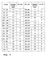
- Figure 5 is a table showing the values of certain outputs at points in the circuit, for input voltages vin within particular ranges.
- the three comparators 18, 19, 20 all output logical "1"s, and so the decode logic block 22 produces an output 11.
- the differential analog voltage vdac+, vdac- is given by vmid, vmid, and this is subtracted from the input voltage vin.
- the resulting voltage is higher than the lowest fine reference value fr1, but lower than the other two fine references fr2, fri, and so the comparators 30, 31, 32 produce outputs 100 respectively.
- These are then decoded in the second decode logic block 34 to produce outputs 01.
- the outputs from the two decode logic blocks are then combined to form an analog-digital converter output 1101.
Landscapes
- Engineering & Computer Science (AREA)
- Theoretical Computer Science (AREA)
- Analogue/Digital Conversion (AREA)
Claims (4)
- Analog/Digital-Wandler (10), der umfasst:einen Eingang (16) für eine analoge Eingangsspannung (vin) innerhalb eines verfügbaren Eingangsspannungsbereiches;eine erste Mehrzahl von Komparatoren (18, 19, 20) zum Vergleichen der analogen Eingangsspannung (vin) mit einer jeweiligen Mehrzahl von Grob-Referenzspannungen (cr1, cr2, cr3), wobei die Grob-Referenzspannungen (cr1, cr2, cr3) den verfügbaren Eingangsspannungsbereich in eine Mehrzahl von Unterbereichen teilen und eine Mitten-Grob-Referenzspannung umfassen;einen ersten Logikblock (22) zum Ausgeben eines ersten digitalen Teilausgangs (mbs1, mbs2) auf der Basis der Vergleiche der analogen Eingangsspannung (vin) mit den Grob-Referenzspannungen (cr1, cr2, cr3);einen Digital/Analog-Wandler (24) zum Erzeugen einer analogen Zwischenspannung (vdac) auf der Basis des ersten digitalen Teilausgangs (msb1, msb2);eine zweite Mehrzahl von Komparatoren (30, 31, 32) zum Vergleichen einer Differenzspannung (vin - vdac), die für eine Differenz zwischen der analogen Eingangsspannung (vin) und der analogen Zwischenspannung (vdac) repräsentativ ist, mit einer jeweiligen Mehrzahl von Fein-Referenzspannungen (fr1, fr2, fr3); undeinen zweiten Logikblock (34) zum Ausgeben eines zweiten digitalen Teilausgangs (lsb1, lsb2) auf der Basis der Vergleiche der Differenzspannung (vin - vdac) mit den Fein-Referenzspannungen (fr1, fr2, fr3);dadurch gekennzeichnet, dassder Digital/Analog-Wandler (24) ausgelegt ist, dieselbe analoge Zwischenspannung (vdac) für analoge Eingangsspannungen in einem ersten Unterbereich unmittelbar oberhalb der Mitten-Grob-Referenzspannung und einem zweiten Unterbereich unmittelbar unterhalb der Mitten-Grob-Referenzspannung zu erzeugen; undwobei die Fein-Referenzspannurigen (fr1, fr2, fr3) auf der Basis des ersten digitalen Teilausgangs (msb1, msb2) ausgewählt werden, derart, dass die ausgewählten Fein-Referenzspannungen (fr1, fr2, fr3) im Fall von oberhalb der Mitten-Grob-Referenzspannung liegenden analogen Eingangsspannungen relativ zu den im Fall von unterhalb der Mitten-Grob-Referenzspannung liegenden analogen Eingangsspannungen ausgewählten Fein-Referenzspannungen (fr1, fr2, fr3) invertiert werden.
- Analog/Digital-Wandler (10) gemäß Anspruch 1, wobei die analoge Eingangsspannung (vin) und die Grob-Referenzspannungen differentielle Spannungen sind und die erste Mehrzahl von Komparatoren (18, 19, 20) differentielle Komparatoren sind.
- Analog/Digital-Wandler (10) gemäß Anspruch 1 oder 2, wobei die analoge Zwischenspannung und die Fein-Referenzspannungen (fr1, fr2, fr3) differentielle Spannungen sind und die zweite Mehrzahl von Komparatoren (30, 31, 32) differentielle Komparatoren sind.
- Analog/Digital-Wandler (10) gemäß einem der vorhergehenden Anspruche, der ferner eine Widerstandsleiter (42) umfasst, um die Grob-Referenzspannungen (cr1, cr2, cr3), die Fein-Referenzspannungen (fr1, fr2, fr3) und die analoge Zwischenspannung (vdac) zu erzeugen.
Priority Applications (2)
| Application Number | Priority Date | Filing Date | Title |
|---|---|---|---|
| DE2003607228 DE60307228T2 (de) | 2003-04-10 | 2003-04-10 | In Unterbereiche aufgeteilter Analog/Digitalwandler mit erhöhter Abtastgenauigkeit und geringer Verzerrung |
| EP20030008345 EP1467490B1 (de) | 2003-04-10 | 2003-04-10 | In Unterbereiche aufgeteilter Analog/Digitalwandler mit erhöhter Abtastgenauigkeit und geringer Verzerrung |
Applications Claiming Priority (1)
| Application Number | Priority Date | Filing Date | Title |
|---|---|---|---|
| EP20030008345 EP1467490B1 (de) | 2003-04-10 | 2003-04-10 | In Unterbereiche aufgeteilter Analog/Digitalwandler mit erhöhter Abtastgenauigkeit und geringer Verzerrung |
Publications (2)
| Publication Number | Publication Date |
|---|---|
| EP1467490A1 EP1467490A1 (de) | 2004-10-13 |
| EP1467490B1 true EP1467490B1 (de) | 2006-08-02 |
Family
ID=32864987
Family Applications (1)
| Application Number | Title | Priority Date | Filing Date |
|---|---|---|---|
| EP20030008345 Expired - Lifetime EP1467490B1 (de) | 2003-04-10 | 2003-04-10 | In Unterbereiche aufgeteilter Analog/Digitalwandler mit erhöhter Abtastgenauigkeit und geringer Verzerrung |
Country Status (2)
| Country | Link |
|---|---|
| EP (1) | EP1467490B1 (de) |
| DE (1) | DE60307228T2 (de) |
Family Cites Families (4)
| Publication number | Priority date | Publication date | Assignee | Title |
|---|---|---|---|---|
| US3597761A (en) * | 1969-11-14 | 1971-08-03 | American Astronics Inc | High-speed analog-to-digital converter and method therefor |
| KR100235465B1 (ko) * | 1996-05-29 | 1999-12-15 | 유기범 | 플래시형 아날로그-디지탈 변환기 |
| US6121912A (en) * | 1998-09-30 | 2000-09-19 | National Semiconductor Corporation | Subranging analog-to-digital converter and method |
| JP4110681B2 (ja) * | 1999-08-02 | 2008-07-02 | ソニー株式会社 | ディジタル/アナログ変換回路及びそれを用いたアナログ/ディジタル変換回路 |
-
2003
- 2003-04-10 EP EP20030008345 patent/EP1467490B1/de not_active Expired - Lifetime
- 2003-04-10 DE DE2003607228 patent/DE60307228T2/de not_active Expired - Fee Related
Also Published As
| Publication number | Publication date |
|---|---|
| DE60307228T2 (de) | 2007-07-26 |
| DE60307228D1 (de) | 2006-09-14 |
| EP1467490A1 (de) | 2004-10-13 |
Similar Documents
| Publication | Publication Date | Title |
|---|---|---|
| EP3322096B1 (de) | Dac-kondensator-array, sar-analog-digital-wandler und verfahren zur verringerung des stromverbrauchs | |
| US10735008B2 (en) | Comparator offset voltage self-correction circuit | |
| US6069579A (en) | Folding type A/D converter and folding type A/D converter circuit | |
| US6346899B1 (en) | Analog current mode D/A converter using transconductors | |
| EP0493443B1 (de) | Paralleler ad-wandler mit 2n-1-vergleichern | |
| US5936566A (en) | Auto-reference pseudo-flash analog to digital converter | |
| US7767953B2 (en) | Voltage generator, analog-to-digital converter, and image sensor system | |
| US7486218B2 (en) | Cyclic analog-to-digital converter | |
| WO1995017782A1 (en) | Analog-to-digital conversion circuit with improved differential linearity | |
| EP1393447B1 (de) | Kapazitive faltschaltung zur verwendung in einem faltungs-interpolations-analog/digital-umsetzer | |
| EP0414389A1 (de) | Seriell-Paralleler Analog/Digital Konverter | |
| KR20000028902A (ko) | 아날로그 디지털 변환기 | |
| EP0383151B1 (de) | Mehrstufen-"Flash"-Analog-Digital-Converter mit Spannungsbewertung | |
| EP2894787A1 (de) | Analog-Digital-Wandler mit sukzessiver Hochgeschwindigkeitsannäherung | |
| US6259392B1 (en) | Multiplying digital-to-analog converters and methods that selectively connect unit and feedback capacitors to reference voltages and feedback voltages | |
| US9143156B1 (en) | High-resolution digital to analog converter | |
| JPH1041824A (ja) | D/a変換器及びa/d変換器 | |
| JPS6387022A (ja) | アナログ・デジタル変換器 | |
| US6288662B1 (en) | A/D converter circuit having ladder resistor network with alternating first and second resistors of different resistance values | |
| KR20140015048A (ko) | 저전압 구동용 dc/dc 변압기가 내장된 아날로그 디지털 변환기 | |
| JP2995599B2 (ja) | アナログデジタル変換方法 | |
| JP4110681B2 (ja) | ディジタル/アナログ変換回路及びそれを用いたアナログ/ディジタル変換回路 | |
| JPH02268521A (ja) | A/d変換方法及びa/d変換装置 | |
| US6304203B1 (en) | Successive approximation AD converter and microcomputer incorporating the same | |
| US6646585B2 (en) | Flash analog-to-digital converter |
Legal Events
| Date | Code | Title | Description |
|---|---|---|---|
| PUAI | Public reference made under article 153(3) epc to a published international application that has entered the european phase |
Free format text: ORIGINAL CODE: 0009012 |
|
| AK | Designated contracting states |
Kind code of ref document: A1 Designated state(s): AT BE BG CH CY CZ DE DK EE ES FI FR GB GR HU IE IT LI LU MC NL PT RO SE SI SK TR |
|
| AX | Request for extension of the european patent |
Extension state: AL LT LV MK |
|
| 17P | Request for examination filed |
Effective date: 20050413 |
|
| AKX | Designation fees paid |
Designated state(s): DE GB |
|
| GRAP | Despatch of communication of intention to grant a patent |
Free format text: ORIGINAL CODE: EPIDOSNIGR1 |
|
| GRAS | Grant fee paid |
Free format text: ORIGINAL CODE: EPIDOSNIGR3 |
|
| GRAA | (expected) grant |
Free format text: ORIGINAL CODE: 0009210 |
|
| AK | Designated contracting states |
Kind code of ref document: B1 Designated state(s): DE GB |
|
| REG | Reference to a national code |
Ref country code: GB Ref legal event code: FG4D |
|
| REF | Corresponds to: |
Ref document number: 60307228 Country of ref document: DE Date of ref document: 20060914 Kind code of ref document: P |
|
| PLBE | No opposition filed within time limit |
Free format text: ORIGINAL CODE: 0009261 |
|
| STAA | Information on the status of an ep patent application or granted ep patent |
Free format text: STATUS: NO OPPOSITION FILED WITHIN TIME LIMIT |
|
| PGFP | Annual fee paid to national office [announced via postgrant information from national office to epo] |
Ref country code: DE Payment date: 20070619 Year of fee payment: 5 |
|
| 26N | No opposition filed |
Effective date: 20070503 |
|
| PGFP | Annual fee paid to national office [announced via postgrant information from national office to epo] |
Ref country code: GB Payment date: 20070426 Year of fee payment: 5 |
|
| GBPC | Gb: european patent ceased through non-payment of renewal fee |
Effective date: 20080410 |
|
| PG25 | Lapsed in a contracting state [announced via postgrant information from national office to epo] |
Ref country code: DE Free format text: LAPSE BECAUSE OF NON-PAYMENT OF DUE FEES Effective date: 20081101 |
|
| PG25 | Lapsed in a contracting state [announced via postgrant information from national office to epo] |
Ref country code: GB Free format text: LAPSE BECAUSE OF NON-PAYMENT OF DUE FEES Effective date: 20080410 |