EP1458012A2 - Ultraviolet light irradiating method and an apparatus using the same - Google Patents
Ultraviolet light irradiating method and an apparatus using the same Download PDFInfo
- Publication number
- EP1458012A2 EP1458012A2 EP04003567A EP04003567A EP1458012A2 EP 1458012 A2 EP1458012 A2 EP 1458012A2 EP 04003567 A EP04003567 A EP 04003567A EP 04003567 A EP04003567 A EP 04003567A EP 1458012 A2 EP1458012 A2 EP 1458012A2
- Authority
- EP
- European Patent Office
- Prior art keywords
- work piece
- ultraviolet
- ultraviolet irradiating
- wafer
- irradiating apparatus
- Prior art date
- Legal status (The legal status is an assumption and is not a legal conclusion. Google has not performed a legal analysis and makes no representation as to the accuracy of the status listed.)
- Granted
Links
Images


Classifications
-
- A—HUMAN NECESSITIES
- A47—FURNITURE; DOMESTIC ARTICLES OR APPLIANCES; COFFEE MILLS; SPICE MILLS; SUCTION CLEANERS IN GENERAL
- A47G—HOUSEHOLD OR TABLE EQUIPMENT
- A47G19/00—Table service
- A47G19/12—Vessels or pots for table use
- A47G19/18—Containers for delivering jam, mustard, or the like
- A47G19/186—Containers for delivering jam, mustard, or the like combined with a spreading implement
-
- H—ELECTRICITY
- H10—SEMICONDUCTOR DEVICES; ELECTRIC SOLID-STATE DEVICES NOT OTHERWISE PROVIDED FOR
- H10P—GENERIC PROCESSES OR APPARATUS FOR THE MANUFACTURE OR TREATMENT OF DEVICES COVERED BY CLASS H10
- H10P72/00—Handling or holding of wafers, substrates or devices during manufacture or treatment thereof
- H10P72/04—Apparatus for manufacture or treatment
- H10P72/0442—Apparatus for placing on an insulating substrate, e.g. tape
-
- H—ELECTRICITY
- H10—SEMICONDUCTOR DEVICES; ELECTRIC SOLID-STATE DEVICES NOT OTHERWISE PROVIDED FOR
- H10P—GENERIC PROCESSES OR APPARATUS FOR THE MANUFACTURE OR TREATMENT OF DEVICES COVERED BY CLASS H10
- H10P72/00—Handling or holding of wafers, substrates or devices during manufacture or treatment thereof
- H10P72/04—Apparatus for manufacture or treatment
- H10P72/0431—Apparatus for thermal treatment
- H10P72/0436—Apparatus for thermal treatment mainly by radiation
-
- A—HUMAN NECESSITIES
- A47—FURNITURE; DOMESTIC ARTICLES OR APPLIANCES; COFFEE MILLS; SPICE MILLS; SUCTION CLEANERS IN GENERAL
- A47G—HOUSEHOLD OR TABLE EQUIPMENT
- A47G2400/00—Details not otherwise provided for in A47G19/00-A47G23/16
- A47G2400/02—Hygiene
Definitions
- This invention relates to an ultraviolet irradiating apparatus for emitting ultraviolet light toward a work piece such as a semiconductor wafer or electronic part and a frame holding the work piece through an ultraviolet sensitive adhesive tape applied to the back surface of the work piece.
- wafers In a conventional process of manufacturing semiconductor wafers (hereinafter simply called “wafers”) or electronic parts, work pieces are processed as held with an ultraviolet sensitive adhesive tape applied thereto.
- the semiconductor manufacturing process includes a dicing step for cutting a wafer into chips, for example.
- the wafer is mounted centrally of a ring-shaped frame, and held (supported) with an ultraviolet sensitive adhesive tape applied to the back surface of the wafer in a way to cover the ring-shaped frame as well.
- an ultraviolet sensitive adhesive tape is used because it has strong adhesion for withstanding impacts occurring in time of cutting, and in order to allow cut chips to separate easily from the adhesive tape in a die-bonding step following the dicing step. That is, the adhesive strength of this tape is lowered when irradiated by ultraviolet light, and this property of the tape is utilized.
- a work piece is enclosed in a cover, and an inert gas is fed into its interior.
- a predetermined quantity of ultraviolet light is emitted by opening and closing a shutter disposed between an ultraviolet lamp and the wafer (see Japanese Unexamined Patent Publication No. 6-204335).
- the apparatus using the conventional ultraviolet irradiating method has the following drawbacks.
- the adhesive tape which has once slackened by heat cannot be restored. While a wafer with the adhesive tape in the slack state is transported to the bonding step, the chips could contact each other to be damaged. When sucking chips from a wafer joined with a ring-shaped frame with a suction collet for transport, the collet may fail to suck the chips accurately, thereby damaging the chips.
- This invention has been made having regard to the state of the art noted above, and its principal object is to provide an ultraviolet irradiating method, and an ultraviolet irradiating apparatus using this method, for holding work pieces steadily without deforming an ultraviolet sensitive adhesive tape holding the work pieces.
- an ultraviolet irradiating method for emitting ultraviolet light toward a work piece and a frame holding the work piece through an ultraviolet sensitive adhesive tape applied to a back surface of the work piece, the method comprising a step of emitting ultraviolet light to the work piece while supporting an undersurface of the work piece held by the frame in time of ultraviolet irradiation of the work piece.
- ultraviolet light is emitted toward a work piece held by a frame through an ultraviolet sensitive adhesive tape, while the undersurface of the work piece is supported.
- the parts may be aligned while constantly maintaining the predetermined intervals without narrowing the intervals therebetween. Consequently, when picking up the parts with a suction collet from the adhesive tape, positions of the parts may be recognized accurately to pick up the parts accurately, thereby realizing an improvement in working efficiency.
- the frame preferably, is a ring-shaped frame having an inside diameter of at least 300mm. It is then possible to hold a large work piece of 300mm or more. In this case, it is desirable to support the work piece against displacement. That is, the larger the inside diameter is, the larger area and greater weight of the work piece is borne by the adhesive tape.
- the adhesive tape would tend to slacken easily under the influence of heat in time of ultraviolet irradiation.
- the work piece is a semiconductor wafer, glass component or semiconductor package substrate.
- a downward displacement of such a product held by the frame may be limited in time of ultraviolet irradiation. That is, where a high processing accuracy is needed such as in processing precision components, an excessive stress may be prevented from occurring with each work piece in time of handling, e.g. transporting, the work piece by precluding deformation of the ultraviolet sensitive type adhesive tape.
- an ultraviolet irradiating apparatus for emitting ultraviolet light toward a work piece and a ring-shaped frame holding the work piece through an ultraviolet sensitive adhesive tape applied to a back surface of the work piece, the apparatus comprising a regulating device for limiting a downward displacement of the work piece held by the ring-shaped frame in time of ultraviolet irradiation of the work piece.
- the regulating device limits a downward displacement of the work piece due to a deformation of the adhesive tape. That is, the regulating device prevents a downward displacement of the work piece due to softening of the adhesive tape under the influence of heat in time of ultraviolet irradiation and slackening under the weight of the work piece.
- chips formed by a dicing process are maintained in a substantially horizontal state. Adjoining chips are protected from damage done by mutual contact occurring with slackening of the adhesive tape. Further, the chips are transported in the substantially horizontal state to a bonding step, for allowing a suction collet to hold the chips accurately by suction.
- the parts may be aligned while constantly maintaining the predetermined intervals without narrowing the intervals therebetween. Consequently, when picking up the parts with a suction collet from the adhesive tape, positions of the parts may be recognized accurately to pick up the parts accurately, thereby realizing an improvement in working efficiency.
- the method set out in claim 1 may be implemented effectively.
- a distance from the undersurface of the work piece to the regulating device is set to at most 3mm. This setting is effective for maintaining the work piece supported in a substantially horizontal state by the ring-shaped frame.
- the regulating device is formed of glass plate.
- the glass plate may comprise soda glass or tempax glass. It is further desirable that the glass plate has a thickness of at least 100 ⁇ m.
- Such materials have sufficient rigidity for supporting the work piece in a way to limit a downward displacement thereof. At the same time, these materials are effective for transmitting ultraviolet light to cure the adhesive of the ultraviolet sensitive adhesive tape.
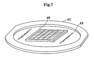
- the regulating device preferably, is formed of metal wires arranged in a grid. It is still more desirable that the metal wires arranged in grid form have a thickness of at most 0.5mm, and have intervals therebetween of at most 20mm.
- the regulating device is formed of a cold filter.
- Such materials have sufficient rigidity for supporting the work piece in a way to limit a downward displacement thereof. At the same time, these materials are effective for transmitting ultraviolet light to cure the adhesive of the ultraviolet sensitive adhesive tape.
- the work piece preferably, is a semiconductor wafer, glass component or semiconductor package substrate. That is, where a high processing accuracy is needed such as in processing precision components, an excessive stress may be prevented from occurring with each work piece in time of handling, e.g. transporting, the work piece by precluding deformation of the ultraviolet sensitive type adhesive tape.
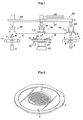
- Fig. 1 is a front view showing an outline of a mechanical portion of an ultraviolet irradiating apparatus according to this invention.
- Fig. 2 is a perspective view of a work piece held by a frame to be processed.
- a semiconductor wafer (hereinafter simply called “wafer”) has an ultraviolet sensitive adhesive tape larger than the wafer applied to the back surface thereof. The adhesive tape is applied at peripheries thereof also to a ring-shaped frame. In this embodiment, the wafer is transported as integrated with the ring-shaped frame.
- the ultraviolet irradiating apparatus in this embodiment includes a work piece loading section A for receiving a ring-shaped frame 3 integrated with a wafer 1 from a dicing apparatus, not shown, disposed in an upstream location, an ultraviolet irradiating section B, and a work piece unloading section C for delivering the wafer 1 after an ultraviolet irradiating process to a treating apparatus, not shown, disposed in a downstream location (e.g. a stocker for storing the processed wafer 1 as held by the ring-shaped frame 3 in an appropriate cassette, or a die bonding apparatus).
- the work piece loading section A may share the stocker with the work piece unloading section C for loading and unloading work pieces into/from cassettes.
- the work piece loading section A includes a loading belt 4 extending along a processing line, and a work piece table 6 vertically movable, with the wafer 1 placed thereon, by an air cylinder 5.
- the work piece unloading section C includes an unloading belt 7 extending along the processing line, and a work piece table 9 vertically movable by an air cylinder 8.
- the ultraviolet irradiating section B as shown in Fig. 1, and in an enlarged view of Fig. 3, includes a ring-shaped support base 10 for receiving a frame portion of the ring-shaped frame 3, a regulating member 11 for limiting a downward displacement of the wafer 1 with the ring-shaped frame 3 supported by the support base 10, a cylindrical housing 12 enclosing the support base 10, an ultraviolet lamp 13 disposed in a lower position for emitting ultraviolet light toward the undersurface of the wafer 1, an ultraviolet flux barrel 14, a shutter 15 and a shutter drive motor 16.
- a cold filter 17 is disposed at the bottom of the support base 10 for shielding infrared light.
- the regulating member 11 which forms a characterizing portion of the apparatus in this embodiment, serves to maintain the wafer 1 held by the ring-shaped frame 3 in a substantially horizontal posture against the adhesive tape 2 softening under the influence of heat in time of ultraviolet irradiation and slackening under the weight of the wafer 1.
- the regulating member 11 sets a gap G not exceeding 3mm from its surface to the adhesive tape attaching surface of the wafer 1 in horizontal posture. A gap exceeding 3mm would allow the adhesive tape 2 to slacken with the heat and the weight of wafer 1. Thus, it would be impossible to hold the wafer 1 in a substantially horizontal posture.
- the regulating member 11 may be formed of any suitable material that transmits ultraviolet light, such as soda glass or tempax glass. It is also possible to use the cold filter 17 as the regulating member 11.
- the thickness preferably, is at least 100 ⁇ m. With a thickness less than 100 ⁇ m, the regulating member 11 would have insufficient rigidity and would not be able to support reliably, in a positionally adjusted state, a large and heavy 300mm wafer 1, for example. It is desirable to use a polyester film or sheet of 150 ⁇ m or lager.
- the ring-shaped frame 3 used for holding the wafer 1 has an inside diameter of at least 300mm.
- a work piece suction mechanism 18 has a plurality of (e.g. four) suction pads 19 for supporting the ring-shaped frame 3 by suction.
- the wafer 1 and ring-shaped frame 3 are placed in a processing chamber 20 in time of ultraviolet irradiation.
- a cover plate 21 is disposed above the suction pads 19 for closing the processing chamber 20 when filling the processing chamber 20 with nitrogen gas for ultraviolet irradiation.
- the apparatus in this embodiment includes a traverse mechanism 22 for suction-supporting and transporting the ring-shaped frame 3 integrated with the wafer 1 from the work piece loading section A to the ultraviolet irradiating section B and from the ultraviolet irradiating section B to the work piece unloading section C.
- This traverse mechanism 22 includes a movable frame 27 having two work piece suction mechanisms 18 and 26 attached to opposite ends thereof to be vertically movable by air cylinders 23 and 24, respectively.
- the movable frame 27 is moved by an air cylinder 28 forward and backward along a guide rail 29 extending along the processing line.
- One of the suction mechanisms 18 feeds a wafer 1 from the work piece loading section A to the ultraviolet irradiating section B, while the other suction mechanism 26 deliver a wafer 1' processed in the ultraviolet irradiating section B to the work piece unloading section C.
- a wafer 1 having undergone a dicing process and joined with the ring-shaped frame 3 is transported to the ultraviolet irradiating section B and received by the support base 10.
- the regulating member 11 limits a downward displacement of the wafer 1 so that it does not fall below a predetermined height. That is, when the ultraviolet lamp 13 emits ultraviolet light, the ultraviolet sensitive adhesive tape 2 softens under the influence of heat and expands under the weight of the wafer 1. The regulating member 11 prevents a descent (displacement) of the wafer 1 occurring at this time.
- the wafer 1 is held by the ring-shaped frame 3 through the adhesive tape 2 in a substantially horizontal state.
- corners of adjoining chips formed after a dicing process are protected from damage done by mutual contact.
- the processed wafer 1 is transported in the substantially horizontal state after the adhesive is cured by ultraviolet irradiation in the ultraviolet irradiating section B.
- a suction collet can transport chips by accurately holding the chips by suction without damage to the corners of the chips.
- the chips may be maintained in an aligned state with predetermined intervals constantly secured instead of reducing the intervals.
- positions of the chips may be recognized accurately, thereby realizing an improvement in working efficiency.
Landscapes
- Engineering & Computer Science (AREA)
- Food Science & Technology (AREA)
- Container, Conveyance, Adherence, Positioning, Of Wafer (AREA)
- Dicing (AREA)
- Physical Or Chemical Processes And Apparatus (AREA)
- Mechanical Treatment Of Semiconductor (AREA)
Abstract
Description
Claims (15)
- An ultraviolet irradiating method for emitting ultraviolet light toward a work piece and a frame holding said work piece through an ultraviolet sensitive adhesive tape applied to a back surface of the work piece, said method comprising:a step of emitting ultraviolet light to said work piece while supporting an undersurface of said work piece held by said frame in time of ultraviolet irradiation of said work piece.
- An ultraviolet irradiating method as defined in claim 1, wherein said frame is a ring-shaped frame having an inside diameter of at least 300mm.
- An ultraviolet irradiating method as defined in claim 1, wherein said work piece is a semiconductor wafer, glass component or semiconductor package substrate.
- An ultraviolet irradiating apparatus for emitting ultraviolet light toward a work piece and a ring-shaped frame holding said work piece through an ultraviolet sensitive adhesive tape applied to a back surface of the work piece, said apparatus comprising:regulating means for limiting a downward displacement of said work piece held by said ring-shaped frame in time of ultraviolet irradiation of said work piece.
- An ultraviolet irradiating apparatus as defined in claim 4, wherein a distance from an undersurface of said work piece to said regulating means is set to at most 3mm.
- An ultraviolet irradiating apparatus as defined in claim 4, wherein said regulating means is formed of glass plate.
- An ultraviolet irradiating apparatus as defined in claim 6, wherein said glass plate comprises soda glass or tempax glass.
- An ultraviolet irradiating apparatus as defined in claim 7, wherein said glass plate has a thickness of at least 100µm.
- An ultraviolet irradiating apparatus as defined in claim 4, wherein said regulating means is formed of a plastic penetrable by ultraviolet light.
- An ultraviolet irradiating apparatus as defined in claim 9, wherein said plastic is a polyester film or polyester sheet.
- An ultraviolet irradiating apparatus as defined in claim 10, wherein said polyester film or polyester sheet has a thickness of at least 150µm.
- An ultraviolet irradiating apparatus as defined in claim 4, wherein said regulating means is formed of metal wires arranged in a grid.
- An ultraviolet irradiating apparatus as defined in claim 12, wherein said metal wires arranged in a grid have a thickness of at most 0.5mm, and have intervals therebetween of at most 20mm.
- An ultraviolet irradiating apparatus as defined in claim 4, wherein said regulating means is formed of a cold filter.
- An ultraviolet irradiating apparatus as defined in claim 4, wherein said work piece is a semiconductor wafer, glass component or semiconductor package substrate.
Applications Claiming Priority (2)
| Application Number | Priority Date | Filing Date | Title |
|---|---|---|---|
| JP2003066561 | 2003-03-12 | ||
| JP2003066561A JP4488686B2 (en) | 2003-03-12 | 2003-03-12 | Ultraviolet irradiation method and apparatus using the same |
Publications (3)
| Publication Number | Publication Date |
|---|---|
| EP1458012A2 true EP1458012A2 (en) | 2004-09-15 |
| EP1458012A3 EP1458012A3 (en) | 2006-05-10 |
| EP1458012B1 EP1458012B1 (en) | 2008-04-02 |
Family
ID=32767936
Family Applications (1)
| Application Number | Title | Priority Date | Filing Date |
|---|---|---|---|
| EP04003567A Expired - Lifetime EP1458012B1 (en) | 2003-03-12 | 2004-02-18 | Ultraviolet light irradiating method and an apparatus using the same |
Country Status (8)
| Country | Link |
|---|---|
| US (1) | US7091499B2 (en) |
| EP (1) | EP1458012B1 (en) |
| JP (1) | JP4488686B2 (en) |
| KR (1) | KR101011890B1 (en) |
| CN (1) | CN100361273C (en) |
| AT (1) | ATE391341T1 (en) |
| DE (1) | DE602004012789T2 (en) |
| TW (1) | TWI312173B (en) |
Families Citing this family (15)
| Publication number | Priority date | Publication date | Assignee | Title |
|---|---|---|---|---|
| JP4641423B2 (en) * | 2004-02-18 | 2011-03-02 | ルネサスエレクトロニクス株式会社 | Semiconductor device and manufacturing method thereof |
| KR100601509B1 (en) | 2004-09-22 | 2006-07-19 | 삼성에스디아이 주식회사 | Case of battery pack |
| JP2006281655A (en) * | 2005-04-01 | 2006-10-19 | Ichikoh Ind Ltd | UV irradiation equipment |
| JP4798754B2 (en) | 2005-05-24 | 2011-10-19 | リンテック株式会社 | Energy beam irradiation apparatus and method |
| JP2007214357A (en) * | 2006-02-09 | 2007-08-23 | Nitto Denko Corp | Work sticking support method and work sticking support apparatus using the same |
| KR100876155B1 (en) * | 2006-11-28 | 2008-12-26 | 삼성전자주식회사 | Wafer protective tape cutting device, back lapping equipment and wafer protective tape cutting method using the same |
| JP5324130B2 (en) | 2008-05-22 | 2013-10-23 | リンテック株式会社 | Light irradiation device |
| JP4796096B2 (en) * | 2008-06-12 | 2011-10-19 | リンテック株式会社 | Light irradiation apparatus and light irradiation method |
| CN103170461B (en) * | 2009-08-07 | 2015-04-08 | 晶元光电股份有限公司 | Chip classification method |
| JP5583374B2 (en) * | 2009-09-07 | 2014-09-03 | 株式会社島津製作所 | Photo-curing resin characteristic testing device, holder used in the testing device, and characteristic testing method |
| US8710458B2 (en) * | 2010-10-19 | 2014-04-29 | Taiwan Semiconductor Manufacturing Company, Ltd. | UV exposure method for reducing residue in de-taping process |
| JP5585379B2 (en) | 2010-10-21 | 2014-09-10 | 富士電機株式会社 | Semiconductor device manufacturing method and manufacturing apparatus thereof |
| KR102516339B1 (en) | 2018-04-06 | 2023-03-31 | 삼성전자주식회사 | Cover structure for a ray illuminator, ray illuminating apparatus having the same and a method of bonding a die to a substrate |
| JP7584259B2 (en) * | 2020-09-07 | 2024-11-15 | 株式会社ディスコ | Ultraviolet irradiation equipment |
| JP2023182043A (en) * | 2022-06-14 | 2023-12-26 | リンテック株式会社 | Electromagnetic wave irradiation device and electromagnetic wave irradiation method |
Family Cites Families (13)
| Publication number | Priority date | Publication date | Assignee | Title |
|---|---|---|---|---|
| JPS5921038A (en) | 1982-07-27 | 1984-02-02 | Nec Home Electronics Ltd | Releasing method for pellet |
| JPS61226933A (en) | 1985-03-30 | 1986-10-08 | Toshiba Corp | Mounting apparatus |
| JPH03180049A (en) | 1989-12-08 | 1991-08-06 | Sumitomo Electric Ind Ltd | Method for picking up semiconductor device |
| US5298365A (en) * | 1990-03-20 | 1994-03-29 | Hitachi, Ltd. | Process for fabricating semiconductor integrated circuit device, and exposing system and mask inspecting method to be used in the process |
| JPH06204335A (en) * | 1993-01-06 | 1994-07-22 | Nitto Denko Corp | Ultraviolet ray radiating device |
| US5435876A (en) * | 1993-03-29 | 1995-07-25 | Texas Instruments Incorporated | Grid array masking tape process |
| JPH08107088A (en) * | 1994-10-04 | 1996-04-23 | Fujitsu Ltd | Method for manufacturing semiconductor device |
| US5590787A (en) * | 1995-01-04 | 1997-01-07 | Micron Technology, Inc. | UV light sensitive die-pac for securing semiconductor dies during transport |
| GB9509487D0 (en) * | 1995-05-10 | 1995-07-05 | Ici Plc | Micro relief element & preparation thereof |
| JP3518786B2 (en) | 1995-12-02 | 2004-04-12 | リンテック株式会社 | Light irradiation device and light irradiation method for dicing tape |
| JP3464596B2 (en) * | 1996-09-13 | 2003-11-10 | 富士通株式会社 | Semiconductor device manufacturing method and manufacturing apparatus |
| US6202292B1 (en) * | 1998-08-26 | 2001-03-20 | Micron Technology, Inc. | Apparatus for removing carrier film from a semiconductor die |
| JP3504543B2 (en) | 1999-03-03 | 2004-03-08 | 株式会社日立製作所 | Semiconductor device separation method and device, and semiconductor device mounting method |
-
2003
- 2003-03-12 JP JP2003066561A patent/JP4488686B2/en not_active Expired - Fee Related
-
2004
- 2004-02-12 US US10/776,221 patent/US7091499B2/en not_active Expired - Fee Related
- 2004-02-18 EP EP04003567A patent/EP1458012B1/en not_active Expired - Lifetime
- 2004-02-18 AT AT04003567T patent/ATE391341T1/en not_active IP Right Cessation
- 2004-02-18 DE DE602004012789T patent/DE602004012789T2/en not_active Expired - Fee Related
- 2004-03-05 KR KR1020040014990A patent/KR101011890B1/en not_active Expired - Fee Related
- 2004-03-10 TW TW093106279A patent/TWI312173B/en not_active IP Right Cessation
- 2004-03-12 CN CNB2004100399041A patent/CN100361273C/en not_active Expired - Fee Related
Also Published As
| Publication number | Publication date |
|---|---|
| JP4488686B2 (en) | 2010-06-23 |
| US20040180515A1 (en) | 2004-09-16 |
| EP1458012A3 (en) | 2006-05-10 |
| KR101011890B1 (en) | 2011-02-01 |
| US7091499B2 (en) | 2006-08-15 |
| JP2004281430A (en) | 2004-10-07 |
| CN1531016A (en) | 2004-09-22 |
| DE602004012789D1 (en) | 2008-05-15 |
| CN100361273C (en) | 2008-01-09 |
| KR20040081012A (en) | 2004-09-20 |
| TWI312173B (en) | 2009-07-11 |
| ATE391341T1 (en) | 2008-04-15 |
| DE602004012789T2 (en) | 2008-07-24 |
| EP1458012B1 (en) | 2008-04-02 |
| TW200425305A (en) | 2004-11-16 |
Similar Documents
| Publication | Publication Date | Title |
|---|---|---|
| US7091499B2 (en) | Ultraviolet irradiating method and an apparatus using the same | |
| US7074646B2 (en) | In-line die attaching and curing apparatus for a multi-chip package | |
| US7406759B2 (en) | Releasing method and releasing apparatus of work having adhesive tape | |
| US20030088959A1 (en) | Wafer transfer apparatus | |
| TWI512877B (en) | Workpiece transport method and workpiece transport device | |
| TWI457976B (en) | Protective tape peeling method and device thereof | |
| KR101720335B1 (en) | Ultraviolet irradiation device | |
| CN108336007B (en) | Frame unit handling system | |
| US20090120589A1 (en) | Semiconductor die bonding apparatus having multiple bonding head units | |
| KR102581316B1 (en) | Transport equipment, substrate processing system, transport method and substrate processing method | |
| JP5312997B2 (en) | UV irradiation equipment | |
| JP6732383B2 (en) | Seat expansion device | |
| KR100849589B1 (en) | Cutting device | |
| KR930001495B1 (en) | Semiconductor wafer processing system | |
| US20080006922A1 (en) | Thermal release adhesive-backed carrier tapes | |
| CN107225700A (en) | The operating method of package substrate | |
| JPH08288318A (en) | Pickup method and device | |
| JP5847410B2 (en) | Die bonder and semiconductor manufacturing method | |
| KR20060044663A (en) | Ultra thin chip manufacturing process and manufacturing apparatus | |
| TWI724246B (en) | Conveying device, processing device and conveying method | |
| JP2024014456A (en) | processing equipment | |
| JP2026001810A (en) | Processing device and processing method | |
| JP3442995B2 (en) | Manufacturing method and manufacturing apparatus for electronic component device | |
| KR20040037815A (en) | Apparatus for irradiating UV and attaching die | |
| JP2022034480A (en) | Processing device |
Legal Events
| Date | Code | Title | Description |
|---|---|---|---|
| PUAI | Public reference made under article 153(3) epc to a published international application that has entered the european phase |
Free format text: ORIGINAL CODE: 0009012 |
|
| AK | Designated contracting states |
Kind code of ref document: A2 Designated state(s): AT BE BG CH CY CZ DE DK EE ES FI FR GB GR HU IE IT LI LU MC NL PT RO SE SI SK TR |
|
| AX | Request for extension of the european patent |
Extension state: AL LT LV MK |
|
| PUAL | Search report despatched |
Free format text: ORIGINAL CODE: 0009013 |
|
| AK | Designated contracting states |
Kind code of ref document: A3 Designated state(s): AT BE BG CH CY CZ DE DK EE ES FI FR GB GR HU IE IT LI LU MC NL PT RO SE SI SK TR |
|
| AX | Request for extension of the european patent |
Extension state: AL LT LV MK |
|
| 17P | Request for examination filed |
Effective date: 20060704 |
|
| R17C | First examination report despatched (corrected) |
Effective date: 20060901 |
|
| AKX | Designation fees paid |
Designated state(s): AT BE BG CH CY CZ DE DK EE ES FI FR GB GR HU IE IT LI LU MC NL PT RO SE SI SK TR |
|
| 17Q | First examination report despatched |
Effective date: 20060901 |
|
| GRAP | Despatch of communication of intention to grant a patent |
Free format text: ORIGINAL CODE: EPIDOSNIGR1 |
|
| GRAS | Grant fee paid |
Free format text: ORIGINAL CODE: EPIDOSNIGR3 |
|
| GRAA | (expected) grant |
Free format text: ORIGINAL CODE: 0009210 |
|
| AK | Designated contracting states |
Kind code of ref document: B1 Designated state(s): AT BE BG CH CY CZ DE DK EE ES FI FR GB GR HU IE IT LI LU MC NL PT RO SE SI SK TR |
|
| REG | Reference to a national code |
Ref country code: GB Ref legal event code: FG4D |
|
| REG | Reference to a national code |
Ref country code: CH Ref legal event code: EP Ref country code: IE Ref legal event code: FG4D |
|
| REF | Corresponds to: |
Ref document number: 602004012789 Country of ref document: DE Date of ref document: 20080515 Kind code of ref document: P |
|
| RIN2 | Information on inventor provided after grant (corrected) |
Inventor name: OKAWA, YUJI |
|
| ET | Fr: translation filed | ||
| PG25 | Lapsed in a contracting state [announced via postgrant information from national office to epo] |
Ref country code: SI Free format text: LAPSE BECAUSE OF FAILURE TO SUBMIT A TRANSLATION OF THE DESCRIPTION OR TO PAY THE FEE WITHIN THE PRESCRIBED TIME-LIMIT Effective date: 20080402 |
|
| NLV1 | Nl: lapsed or annulled due to failure to fulfill the requirements of art. 29p and 29m of the patents act | ||
| PG25 | Lapsed in a contracting state [announced via postgrant information from national office to epo] |
Ref country code: BG Free format text: LAPSE BECAUSE OF FAILURE TO SUBMIT A TRANSLATION OF THE DESCRIPTION OR TO PAY THE FEE WITHIN THE PRESCRIBED TIME-LIMIT Effective date: 20080702 Ref country code: ES Free format text: LAPSE BECAUSE OF FAILURE TO SUBMIT A TRANSLATION OF THE DESCRIPTION OR TO PAY THE FEE WITHIN THE PRESCRIBED TIME-LIMIT Effective date: 20080713 Ref country code: FI Free format text: LAPSE BECAUSE OF FAILURE TO SUBMIT A TRANSLATION OF THE DESCRIPTION OR TO PAY THE FEE WITHIN THE PRESCRIBED TIME-LIMIT Effective date: 20080402 Ref country code: PT Free format text: LAPSE BECAUSE OF FAILURE TO SUBMIT A TRANSLATION OF THE DESCRIPTION OR TO PAY THE FEE WITHIN THE PRESCRIBED TIME-LIMIT Effective date: 20080903 Ref country code: NL Free format text: LAPSE BECAUSE OF FAILURE TO SUBMIT A TRANSLATION OF THE DESCRIPTION OR TO PAY THE FEE WITHIN THE PRESCRIBED TIME-LIMIT Effective date: 20080402 |
|
| PG25 | Lapsed in a contracting state [announced via postgrant information from national office to epo] |
Ref country code: AT Free format text: LAPSE BECAUSE OF FAILURE TO SUBMIT A TRANSLATION OF THE DESCRIPTION OR TO PAY THE FEE WITHIN THE PRESCRIBED TIME-LIMIT Effective date: 20080402 |
|
| PG25 | Lapsed in a contracting state [announced via postgrant information from national office to epo] |
Ref country code: SE Free format text: LAPSE BECAUSE OF FAILURE TO SUBMIT A TRANSLATION OF THE DESCRIPTION OR TO PAY THE FEE WITHIN THE PRESCRIBED TIME-LIMIT Effective date: 20080702 Ref country code: CZ Free format text: LAPSE BECAUSE OF FAILURE TO SUBMIT A TRANSLATION OF THE DESCRIPTION OR TO PAY THE FEE WITHIN THE PRESCRIBED TIME-LIMIT Effective date: 20080402 Ref country code: DK Free format text: LAPSE BECAUSE OF FAILURE TO SUBMIT A TRANSLATION OF THE DESCRIPTION OR TO PAY THE FEE WITHIN THE PRESCRIBED TIME-LIMIT Effective date: 20080402 |
|
| PLBE | No opposition filed within time limit |
Free format text: ORIGINAL CODE: 0009261 |
|
| STAA | Information on the status of an ep patent application or granted ep patent |
Free format text: STATUS: NO OPPOSITION FILED WITHIN TIME LIMIT |
|
| PG25 | Lapsed in a contracting state [announced via postgrant information from national office to epo] |
Ref country code: SK Free format text: LAPSE BECAUSE OF FAILURE TO SUBMIT A TRANSLATION OF THE DESCRIPTION OR TO PAY THE FEE WITHIN THE PRESCRIBED TIME-LIMIT Effective date: 20080402 Ref country code: RO Free format text: LAPSE BECAUSE OF FAILURE TO SUBMIT A TRANSLATION OF THE DESCRIPTION OR TO PAY THE FEE WITHIN THE PRESCRIBED TIME-LIMIT Effective date: 20080402 |
|
| 26N | No opposition filed |
Effective date: 20090106 |
|
| PG25 | Lapsed in a contracting state [announced via postgrant information from national office to epo] |
Ref country code: EE Free format text: LAPSE BECAUSE OF FAILURE TO SUBMIT A TRANSLATION OF THE DESCRIPTION OR TO PAY THE FEE WITHIN THE PRESCRIBED TIME-LIMIT Effective date: 20080402 |
|
| PGFP | Annual fee paid to national office [announced via postgrant information from national office to epo] |
Ref country code: DE Payment date: 20090213 Year of fee payment: 6 |
|
| PGFP | Annual fee paid to national office [announced via postgrant information from national office to epo] |
Ref country code: BE Payment date: 20090216 Year of fee payment: 6 |
|
| PGFP | Annual fee paid to national office [announced via postgrant information from national office to epo] |
Ref country code: IT Payment date: 20090212 Year of fee payment: 6 |
|
| PG25 | Lapsed in a contracting state [announced via postgrant information from national office to epo] |
Ref country code: MC Free format text: LAPSE BECAUSE OF NON-PAYMENT OF DUE FEES Effective date: 20090228 Ref country code: CY Free format text: LAPSE BECAUSE OF FAILURE TO SUBMIT A TRANSLATION OF THE DESCRIPTION OR TO PAY THE FEE WITHIN THE PRESCRIBED TIME-LIMIT Effective date: 20080402 |
|
| REG | Reference to a national code |
Ref country code: CH Ref legal event code: PL |
|
| GBPC | Gb: european patent ceased through non-payment of renewal fee |
Effective date: 20090218 |
|
| PG25 | Lapsed in a contracting state [announced via postgrant information from national office to epo] |
Ref country code: CH Free format text: LAPSE BECAUSE OF NON-PAYMENT OF DUE FEES Effective date: 20090228 Ref country code: LI Free format text: LAPSE BECAUSE OF NON-PAYMENT OF DUE FEES Effective date: 20090228 |
|
| PGFP | Annual fee paid to national office [announced via postgrant information from national office to epo] |
Ref country code: FR Payment date: 20090213 Year of fee payment: 6 |
|
| PG25 | Lapsed in a contracting state [announced via postgrant information from national office to epo] |
Ref country code: IE Free format text: LAPSE BECAUSE OF NON-PAYMENT OF DUE FEES Effective date: 20090218 |
|
| PG25 | Lapsed in a contracting state [announced via postgrant information from national office to epo] |
Ref country code: GB Free format text: LAPSE BECAUSE OF NON-PAYMENT OF DUE FEES Effective date: 20090218 |
|
| BERE | Be: lapsed |
Owner name: NITTO DENKO CORP. Effective date: 20100228 |
|
| PG25 | Lapsed in a contracting state [announced via postgrant information from national office to epo] |
Ref country code: GR Free format text: LAPSE BECAUSE OF FAILURE TO SUBMIT A TRANSLATION OF THE DESCRIPTION OR TO PAY THE FEE WITHIN THE PRESCRIBED TIME-LIMIT Effective date: 20080703 |
|
| REG | Reference to a national code |
Ref country code: FR Ref legal event code: ST Effective date: 20101029 |
|
| PG25 | Lapsed in a contracting state [announced via postgrant information from national office to epo] |
Ref country code: FR Free format text: LAPSE BECAUSE OF NON-PAYMENT OF DUE FEES Effective date: 20100301 |
|
| PG25 | Lapsed in a contracting state [announced via postgrant information from national office to epo] |
Ref country code: BE Free format text: LAPSE BECAUSE OF NON-PAYMENT OF DUE FEES Effective date: 20100228 Ref country code: DE Free format text: LAPSE BECAUSE OF NON-PAYMENT OF DUE FEES Effective date: 20100901 |
|
| PG25 | Lapsed in a contracting state [announced via postgrant information from national office to epo] |
Ref country code: IT Free format text: LAPSE BECAUSE OF NON-PAYMENT OF DUE FEES Effective date: 20100218 |
|
| PG25 | Lapsed in a contracting state [announced via postgrant information from national office to epo] |
Ref country code: LU Free format text: LAPSE BECAUSE OF NON-PAYMENT OF DUE FEES Effective date: 20090218 |
|
| PG25 | Lapsed in a contracting state [announced via postgrant information from national office to epo] |
Ref country code: HU Free format text: LAPSE BECAUSE OF FAILURE TO SUBMIT A TRANSLATION OF THE DESCRIPTION OR TO PAY THE FEE WITHIN THE PRESCRIBED TIME-LIMIT Effective date: 20081003 |
|
| PG25 | Lapsed in a contracting state [announced via postgrant information from national office to epo] |
Ref country code: TR Free format text: LAPSE BECAUSE OF FAILURE TO SUBMIT A TRANSLATION OF THE DESCRIPTION OR TO PAY THE FEE WITHIN THE PRESCRIBED TIME-LIMIT Effective date: 20080402 |