EP1453364A1 - Film for circuit board - Google Patents
Film for circuit board Download PDFInfo
- Publication number
- EP1453364A1 EP1453364A1 EP02747661A EP02747661A EP1453364A1 EP 1453364 A1 EP1453364 A1 EP 1453364A1 EP 02747661 A EP02747661 A EP 02747661A EP 02747661 A EP02747661 A EP 02747661A EP 1453364 A1 EP1453364 A1 EP 1453364A1
- Authority
- EP
- European Patent Office
- Prior art keywords
- layer
- film
- resin
- heat
- circuit board
- Prior art date
- Legal status (The legal status is an assumption and is not a legal conclusion. Google has not performed a legal analysis and makes no representation as to the accuracy of the status listed.)
- Withdrawn
Links
Images

Classifications
-
- H—ELECTRICITY
- H05—ELECTRIC TECHNIQUES NOT OTHERWISE PROVIDED FOR
- H05K—PRINTED CIRCUITS; CASINGS OR CONSTRUCTIONAL DETAILS OF ELECTRIC APPARATUS; MANUFACTURE OF ASSEMBLAGES OF ELECTRICAL COMPONENTS
- H05K3/00—Apparatus or processes for manufacturing printed circuits
- H05K3/38—Improvement of the adhesion between the insulating substrate and the metal
- H05K3/386—Improvement of the adhesion between the insulating substrate and the metal by the use of an organic polymeric bonding layer, e.g. adhesive
- H05K3/387—Improvement of the adhesion between the insulating substrate and the metal by the use of an organic polymeric bonding layer, e.g. adhesive for electroless plating
-
- H—ELECTRICITY
- H05—ELECTRIC TECHNIQUES NOT OTHERWISE PROVIDED FOR
- H05K—PRINTED CIRCUITS; CASINGS OR CONSTRUCTIONAL DETAILS OF ELECTRIC APPARATUS; MANUFACTURE OF ASSEMBLAGES OF ELECTRICAL COMPONENTS
- H05K1/00—Printed circuits
- H05K1/02—Details
- H05K1/03—Use of materials for the substrate
-
- B—PERFORMING OPERATIONS; TRANSPORTING
- B32—LAYERED PRODUCTS
- B32B—LAYERED PRODUCTS, i.e. PRODUCTS BUILT-UP OF STRATA OF FLAT OR NON-FLAT, e.g. CELLULAR OR HONEYCOMB, FORM
- B32B15/00—Layered products comprising a layer of metal
- B32B15/04—Layered products comprising a layer of metal comprising metal as the main or only constituent of a layer, which is next to another layer of the same or of a different material
- B32B15/08—Layered products comprising a layer of metal comprising metal as the main or only constituent of a layer, which is next to another layer of the same or of a different material of synthetic resin
-
- B—PERFORMING OPERATIONS; TRANSPORTING
- B32—LAYERED PRODUCTS
- B32B—LAYERED PRODUCTS, i.e. PRODUCTS BUILT-UP OF STRATA OF FLAT OR NON-FLAT, e.g. CELLULAR OR HONEYCOMB, FORM
- B32B27/00—Layered products comprising a layer of synthetic resin
- B32B27/06—Layered products comprising a layer of synthetic resin as the main or only constituent of a layer, which is next to another layer of the same or of a different material
- B32B27/08—Layered products comprising a layer of synthetic resin as the main or only constituent of a layer, which is next to another layer of the same or of a different material of synthetic resin
-
- H—ELECTRICITY
- H05—ELECTRIC TECHNIQUES NOT OTHERWISE PROVIDED FOR
- H05K—PRINTED CIRCUITS; CASINGS OR CONSTRUCTIONAL DETAILS OF ELECTRIC APPARATUS; MANUFACTURE OF ASSEMBLAGES OF ELECTRICAL COMPONENTS
- H05K1/00—Printed circuits
- H05K1/02—Details
- H05K1/03—Use of materials for the substrate
- H05K1/0313—Organic insulating material
- H05K1/0353—Organic insulating material consisting of two or more materials, e.g. two or more polymers, polymer + filler, + reinforcement
- H05K1/036—Multilayers with layers of different types
-
- H—ELECTRICITY
- H05—ELECTRIC TECHNIQUES NOT OTHERWISE PROVIDED FOR
- H05K—PRINTED CIRCUITS; CASINGS OR CONSTRUCTIONAL DETAILS OF ELECTRIC APPARATUS; MANUFACTURE OF ASSEMBLAGES OF ELECTRICAL COMPONENTS
- H05K2201/00—Indexing scheme relating to printed circuits covered by H05K1/00
- H05K2201/01—Dielectrics
- H05K2201/0137—Materials
- H05K2201/0141—Liquid crystal polymer [LCP]
-
- H—ELECTRICITY
- H05—ELECTRIC TECHNIQUES NOT OTHERWISE PROVIDED FOR
- H05K—PRINTED CIRCUITS; CASINGS OR CONSTRUCTIONAL DETAILS OF ELECTRIC APPARATUS; MANUFACTURE OF ASSEMBLAGES OF ELECTRICAL COMPONENTS
- H05K2201/00—Indexing scheme relating to printed circuits covered by H05K1/00
- H05K2201/01—Dielectrics
- H05K2201/0137—Materials
- H05K2201/0154—Polyimide
-
- H—ELECTRICITY
- H05—ELECTRIC TECHNIQUES NOT OTHERWISE PROVIDED FOR
- H05K—PRINTED CIRCUITS; CASINGS OR CONSTRUCTIONAL DETAILS OF ELECTRIC APPARATUS; MANUFACTURE OF ASSEMBLAGES OF ELECTRICAL COMPONENTS
- H05K2201/00—Indexing scheme relating to printed circuits covered by H05K1/00
- H05K2201/03—Conductive materials
- H05K2201/0332—Structure of the conductor
- H05K2201/0388—Other aspects of conductors
- H05K2201/0394—Conductor crossing over a hole in the substrate or a gap between two separate substrate parts
-
- H—ELECTRICITY
- H05—ELECTRIC TECHNIQUES NOT OTHERWISE PROVIDED FOR
- H05K—PRINTED CIRCUITS; CASINGS OR CONSTRUCTIONAL DETAILS OF ELECTRIC APPARATUS; MANUFACTURE OF ASSEMBLAGES OF ELECTRICAL COMPONENTS
- H05K2203/00—Indexing scheme relating to apparatus or processes for manufacturing printed circuits covered by H05K3/00
- H05K2203/02—Details related to mechanical or acoustic processing, e.g. drilling, punching, cutting, using ultrasound
- H05K2203/0264—Peeling insulating layer, e.g. foil, or separating mask
-
- H—ELECTRICITY
- H05—ELECTRIC TECHNIQUES NOT OTHERWISE PROVIDED FOR
- H05K—PRINTED CIRCUITS; CASINGS OR CONSTRUCTIONAL DETAILS OF ELECTRIC APPARATUS; MANUFACTURE OF ASSEMBLAGES OF ELECTRICAL COMPONENTS
- H05K3/00—Apparatus or processes for manufacturing printed circuits
- H05K3/10—Apparatus or processes for manufacturing printed circuits in which conductive material is applied to the insulating support in such a manner as to form the desired conductive pattern
- H05K3/18—Apparatus or processes for manufacturing printed circuits in which conductive material is applied to the insulating support in such a manner as to form the desired conductive pattern using precipitation techniques to apply the conductive material
- H05K3/181—Apparatus or processes for manufacturing printed circuits in which conductive material is applied to the insulating support in such a manner as to form the desired conductive pattern using precipitation techniques to apply the conductive material by electroless plating
-
- H—ELECTRICITY
- H05—ELECTRIC TECHNIQUES NOT OTHERWISE PROVIDED FOR
- H05K—PRINTED CIRCUITS; CASINGS OR CONSTRUCTIONAL DETAILS OF ELECTRIC APPARATUS; MANUFACTURE OF ASSEMBLAGES OF ELECTRICAL COMPONENTS
- H05K3/00—Apparatus or processes for manufacturing printed circuits
- H05K3/38—Improvement of the adhesion between the insulating substrate and the metal
- H05K3/381—Improvement of the adhesion between the insulating substrate and the metal by special treatment of the substrate
-
- Y—GENERAL TAGGING OF NEW TECHNOLOGICAL DEVELOPMENTS; GENERAL TAGGING OF CROSS-SECTIONAL TECHNOLOGIES SPANNING OVER SEVERAL SECTIONS OF THE IPC; TECHNICAL SUBJECTS COVERED BY FORMER USPC CROSS-REFERENCE ART COLLECTIONS [XRACs] AND DIGESTS
- Y10—TECHNICAL SUBJECTS COVERED BY FORMER USPC
- Y10S—TECHNICAL SUBJECTS COVERED BY FORMER USPC CROSS-REFERENCE ART COLLECTIONS [XRACs] AND DIGESTS
- Y10S428/00—Stock material or miscellaneous articles
- Y10S428/901—Printed circuit
-
- Y—GENERAL TAGGING OF NEW TECHNOLOGICAL DEVELOPMENTS; GENERAL TAGGING OF CROSS-SECTIONAL TECHNOLOGIES SPANNING OVER SEVERAL SECTIONS OF THE IPC; TECHNICAL SUBJECTS COVERED BY FORMER USPC CROSS-REFERENCE ART COLLECTIONS [XRACs] AND DIGESTS
- Y10—TECHNICAL SUBJECTS COVERED BY FORMER USPC
- Y10T—TECHNICAL SUBJECTS COVERED BY FORMER US CLASSIFICATION
- Y10T428/00—Stock material or miscellaneous articles
- Y10T428/24—Structurally defined web or sheet [e.g., overall dimension, etc.]
- Y10T428/24802—Discontinuous or differential coating, impregnation or bond [e.g., artwork, printing, retouched photograph, etc.]
- Y10T428/24917—Discontinuous or differential coating, impregnation or bond [e.g., artwork, printing, retouched photograph, etc.] including metal layer
-
- Y—GENERAL TAGGING OF NEW TECHNOLOGICAL DEVELOPMENTS; GENERAL TAGGING OF CROSS-SECTIONAL TECHNOLOGIES SPANNING OVER SEVERAL SECTIONS OF THE IPC; TECHNICAL SUBJECTS COVERED BY FORMER USPC CROSS-REFERENCE ART COLLECTIONS [XRACs] AND DIGESTS
- Y10—TECHNICAL SUBJECTS COVERED BY FORMER USPC
- Y10T—TECHNICAL SUBJECTS COVERED BY FORMER US CLASSIFICATION
- Y10T428/00—Stock material or miscellaneous articles
- Y10T428/24—Structurally defined web or sheet [e.g., overall dimension, etc.]
- Y10T428/24942—Structurally defined web or sheet [e.g., overall dimension, etc.] including components having same physical characteristic in differing degree
- Y10T428/2495—Thickness [relative or absolute]
-
- Y—GENERAL TAGGING OF NEW TECHNOLOGICAL DEVELOPMENTS; GENERAL TAGGING OF CROSS-SECTIONAL TECHNOLOGIES SPANNING OVER SEVERAL SECTIONS OF THE IPC; TECHNICAL SUBJECTS COVERED BY FORMER USPC CROSS-REFERENCE ART COLLECTIONS [XRACs] AND DIGESTS
- Y10—TECHNICAL SUBJECTS COVERED BY FORMER USPC
- Y10T—TECHNICAL SUBJECTS COVERED BY FORMER US CLASSIFICATION
- Y10T428/00—Stock material or miscellaneous articles
- Y10T428/26—Web or sheet containing structurally defined element or component, the element or component having a specified physical dimension
- Y10T428/263—Coating layer not in excess of 5 mils thick or equivalent
- Y10T428/264—Up to 3 mils
- Y10T428/265—1 mil or less
-
- Y—GENERAL TAGGING OF NEW TECHNOLOGICAL DEVELOPMENTS; GENERAL TAGGING OF CROSS-SECTIONAL TECHNOLOGIES SPANNING OVER SEVERAL SECTIONS OF THE IPC; TECHNICAL SUBJECTS COVERED BY FORMER USPC CROSS-REFERENCE ART COLLECTIONS [XRACs] AND DIGESTS
- Y10—TECHNICAL SUBJECTS COVERED BY FORMER USPC
- Y10T—TECHNICAL SUBJECTS COVERED BY FORMER US CLASSIFICATION
- Y10T428/00—Stock material or miscellaneous articles
- Y10T428/28—Web or sheet containing structurally defined element or component and having an adhesive outermost layer
- Y10T428/2804—Next to metal
-
- Y—GENERAL TAGGING OF NEW TECHNOLOGICAL DEVELOPMENTS; GENERAL TAGGING OF CROSS-SECTIONAL TECHNOLOGIES SPANNING OVER SEVERAL SECTIONS OF THE IPC; TECHNICAL SUBJECTS COVERED BY FORMER USPC CROSS-REFERENCE ART COLLECTIONS [XRACs] AND DIGESTS
- Y10—TECHNICAL SUBJECTS COVERED BY FORMER USPC
- Y10T—TECHNICAL SUBJECTS COVERED BY FORMER US CLASSIFICATION
- Y10T428/00—Stock material or miscellaneous articles
- Y10T428/28—Web or sheet containing structurally defined element or component and having an adhesive outermost layer
- Y10T428/2852—Adhesive compositions
-
- Y—GENERAL TAGGING OF NEW TECHNOLOGICAL DEVELOPMENTS; GENERAL TAGGING OF CROSS-SECTIONAL TECHNOLOGIES SPANNING OVER SEVERAL SECTIONS OF THE IPC; TECHNICAL SUBJECTS COVERED BY FORMER USPC CROSS-REFERENCE ART COLLECTIONS [XRACs] AND DIGESTS
- Y10—TECHNICAL SUBJECTS COVERED BY FORMER USPC
- Y10T—TECHNICAL SUBJECTS COVERED BY FORMER US CLASSIFICATION
- Y10T428/00—Stock material or miscellaneous articles
- Y10T428/31504—Composite [nonstructural laminate]
- Y10T428/31511—Of epoxy ether
-
- Y—GENERAL TAGGING OF NEW TECHNOLOGICAL DEVELOPMENTS; GENERAL TAGGING OF CROSS-SECTIONAL TECHNOLOGIES SPANNING OVER SEVERAL SECTIONS OF THE IPC; TECHNICAL SUBJECTS COVERED BY FORMER USPC CROSS-REFERENCE ART COLLECTIONS [XRACs] AND DIGESTS
- Y10—TECHNICAL SUBJECTS COVERED BY FORMER USPC
- Y10T—TECHNICAL SUBJECTS COVERED BY FORMER US CLASSIFICATION
- Y10T428/00—Stock material or miscellaneous articles
- Y10T428/31504—Composite [nonstructural laminate]
- Y10T428/31511—Of epoxy ether
- Y10T428/31515—As intermediate layer
-
- Y—GENERAL TAGGING OF NEW TECHNOLOGICAL DEVELOPMENTS; GENERAL TAGGING OF CROSS-SECTIONAL TECHNOLOGIES SPANNING OVER SEVERAL SECTIONS OF THE IPC; TECHNICAL SUBJECTS COVERED BY FORMER USPC CROSS-REFERENCE ART COLLECTIONS [XRACs] AND DIGESTS
- Y10—TECHNICAL SUBJECTS COVERED BY FORMER USPC
- Y10T—TECHNICAL SUBJECTS COVERED BY FORMER US CLASSIFICATION
- Y10T428/00—Stock material or miscellaneous articles
- Y10T428/31504—Composite [nonstructural laminate]
- Y10T428/31511—Of epoxy ether
- Y10T428/31515—As intermediate layer
- Y10T428/31522—Next to metal
-
- Y—GENERAL TAGGING OF NEW TECHNOLOGICAL DEVELOPMENTS; GENERAL TAGGING OF CROSS-SECTIONAL TECHNOLOGIES SPANNING OVER SEVERAL SECTIONS OF THE IPC; TECHNICAL SUBJECTS COVERED BY FORMER USPC CROSS-REFERENCE ART COLLECTIONS [XRACs] AND DIGESTS
- Y10—TECHNICAL SUBJECTS COVERED BY FORMER USPC
- Y10T—TECHNICAL SUBJECTS COVERED BY FORMER US CLASSIFICATION
- Y10T428/00—Stock material or miscellaneous articles
- Y10T428/31504—Composite [nonstructural laminate]
- Y10T428/31511—Of epoxy ether
- Y10T428/31529—Next to metal
Definitions
- the present invention relates to a film for a circuit board, especially a film for a circuit board which can be utilized in an electronic circuit and the like of portable devices such as a cellular phone, PDA (personal digital assistant), a notebook personal computer and the like, particularly a film suitable for a flexible circuit board.
- portable devices such as a cellular phone, PDA (personal digital assistant), a notebook personal computer and the like, particularly a film suitable for a flexible circuit board.
- Polyimide resin films, liquid crystal polymer films, aramid resin films, polyether ether ketone films and the like have found wide acceptance as insulation materials of electronic devices and the like because they are excellent in heat resistance, dimensional stability, solvent resistance and electrical and mechanical properties.
- a product in which a conductor layer is formed on a polyimide resin film has often been used in the flexible printedcircuit boards (FPC) of tape automated bonding (TAB) or the like.
- a copper foil having a certain thickness of, for example, 35 ⁇ m, 18 ⁇ m or 12 ⁇ m is used.
- the thickness is increased, formation of a fine circuit by a subtractive method is difficult, whereas when the thickness is decreased, the cost is increased.
- the thickness is increased by plating a copper foil as well which is disadvantageous for formation of a fine circuit.
- the former requires formation of a metallic layer of cobalt, nickel or chromium as a base by a dry metalizing method such as sputtering or vacuum deposition for improving adhesion between the polyimide resin film and the conductor layer.
- a dry metalizing method such as sputtering or vacuum deposition for improving adhesion between the polyimide resin film and the conductor layer.
- the step is complicated and it is difficult to prevent generation of pinholes.
- the latter also requires a step of electroless nickel plating or the like prior to electroless copper plating or electroplating copper step in addition to special hydrophilic treatment on the surface of the polyimide resin film.
- the step is complicated, and adhesion strength is not necessarily at a satisfactory level.
- the invention aims to provide a film for producing simply a circuit board excellent in adhesion strength of a conductor layer, and further a film for a circuit board appropriate for formation of a fine printed circuit.
- the present inventors have assiduously conducted investigations for solving the foregoing problems, and have consequently found that a circuit board with a conductor layer excellent in adhesion can easily be produced from a film in which a specific roughenable cured resin layer is formed on a heat-resistant resin layer of a specific polyimide resin, liquid crystal polymer or the like through a general-purpose process of roughening, electroless copper plating and electroplating copper, and further that the film becomes a film suitable for a circuit board that allows formation of a fine printed circuit.
- the invention has been completed on the basis of such findings.
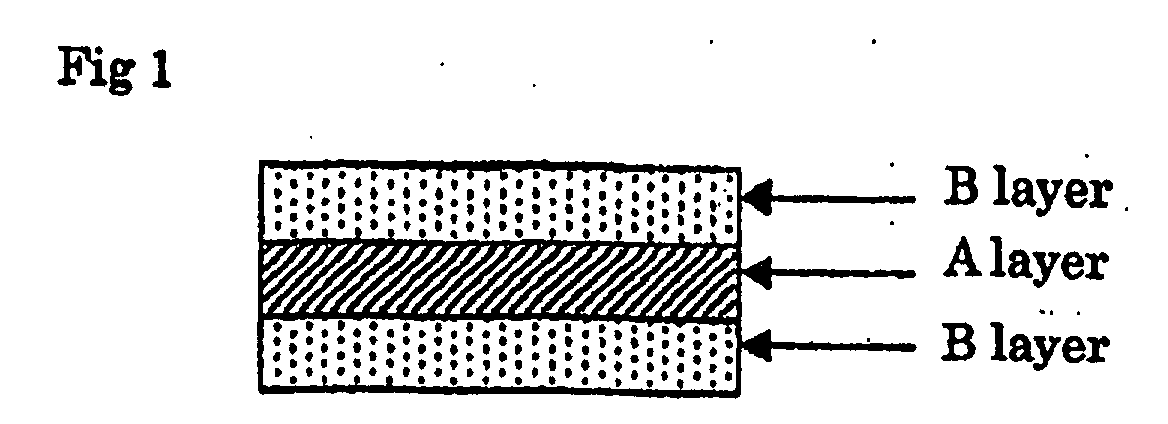
- the invention relates to a film for a circuit board characterized in that the following A layer is adjacent to the following B layer.
- the film for a circuit board in the invention has "a heat-resistant resin layer with a thickness of from 2 to 250 ⁇ m which layer is made of a heat-resistant resin having a glass transition point of 200°C or more or a decomposition temperature of 300°C or more” (which is sometimes abbreviated as “A layer” or “heat-resistant resin layer” in the present specification).
- the heat-resistant resin used in the invention has a glass transition point of 200°C or more or a decomposition temperature of 300°C or more which satisfies heat resistance in soldering required in the production of a multilayer printed wiring board.
- the decomposition temperature is defined in terms of a temperature at which the weight reduction rate becomes 5% when measured according to JIS (Japanese Industrial Standards) K 7120 (gravimetry of plastics).
- the heat-resistant resin comprising the heat-resistant resin layer is preferably selected from a polyimide resin, a liquid crystal polymer, an aramid resin and a polyether ether ketone. Especially, a polyimide resin is preferable.
- a liquid crystal polymer a liquid crystal polymer which is structurally a wholly aromatic polyester is preferably used.
- the thickness of the heat-resistant resin layer is less than 2 ⁇ m, mechanical strength of an insulation layer or a multilayer printed wiring board might be insufficient. When it exceeds 250 ⁇ m, the cost is increased, and the thickness of the insulation layer becomes more than is required. Thus, these are undesirable.
- a layer for a flexible printed circuit board a layer having a thickness of from 2 to 75 ⁇ m is ordinarily used. A layer having a thickness of from 75 to 250 ⁇ m is suitable for use in, for example, an interposer of CSP (chip-size package).
- heat-resistant resin films such as a polyimide film "Upilex-S” manufactured by Ube Industries, Ltd., a polyimide film “Kapton” manufactured by Du Pont-Toray Co., Ltd., a polyimide film "Apical” manufactured by Kaneka Corporation, an aramid film “Aramica” manufactured by Asahi Kasei Corporation, anaramid film “Mictron” manufactured by Toray Industries Inc., a liquid crystal polymer film “Vecstar” manufactured by Kuraray Co. , Ltd. and a polyether ether ketone film “Sumilite FS-1100C” manufactured by Sumitomo Bakelite Co., Ltd. are available.
- a polyimide film "Upilex-S” manufactured by Ube Industries, Ltd. a polyimide film "Kapton” manufactured by Du Pont-Toray Co., Ltd.
- a polyimide film "Apical” manufactured by Kaneka Corporation an aramid film “Aramica” manufactured by Asahi Kas
- a surface-treated layer may be used as the heat-resistant resin layer (A layer).
- the surface treatment include dry treatments such as corona discharge, plasma treatment and ion beam treatment, chemical treatments with a solvent, an acid and an alkali, mechanical polishing and the like.
- plasma treatment it is preferable to apply plasma treatment.
- the film for a circuit board in the invention has also "a roughenable cured resin layer with a thickness of from 5 to 20 ⁇ m which layer is made of a cured product of a thermosetting resin composition containing at least component (a) of an epoxy resin having two or more epoxy groups in a molecule and component (b) of an epoxy curing agent, the cured product being capable of roughening with an oxidizing agent” (which is sometimes abbreviated as B layer or “roughenable cured resin layer” in the present specification). This is described below.
- an aromatic epoxy resin having an aromatic ring structure in a molecule is preferably used for increasing the heat resistance.
- examples thereof can include epoxy resins having two or more epoxy groups in a molecule, such as a bisphenol A-type epoxy resin, a bisphenol F-type epoxy resin, a phenolic novolak-type epoxy resin, a bisphenol S-type epoxy resin, an alkylphenolic novolak-type epoxy resin, a biphenol-type epoxy resin, a naphthalene-type epoxy resin, an epoxy compound of a condensate of a phenol and an aromatic aldehyde having a phenolic hydroxyl group, and the like.
- the epoxy resin may be brominated or the like for imparting fire retardance.
- epoxy curing agent as component (b) can include an amine-type curing agent, a guanidine-type curing agent, an imidazole-type curing agent, a phenolic curing agent, an acid anhydride-type curing agent, epoxy adducts or microcapsules thereof, and the like. Further, with respect to the curing agents, those having a longer pot life are preferable. Two or more of the epoxy curing agents can also be used in combination.
- epoxy curing agents can include dicyandiamide, 2-phenyl-4-methyl-5-hydroxymethylimidazole, 2-phenyl-4,5-bis(hydroxymethyl)imidazole, 2,4-diamino-6-(2-methyl-1-imidazolylethyl)-1,3,5-triazine isocyanuric acid adduct, 2,4-diamino-6-(2-undecyl-1-imidazolylethyl)-1,3,5-triazine and the like.
- the phenolic curing agent having a nitrogen atom is especially preferable.
- the use of the phenolic curing agent having the nitrogen atom is effective for improving heat resistance, fire retardance and adhesion of the insulation layer.
- Examples of such an epoxy curing agent can include a triazine structure-containing novolak resin (for example, "Phenolite 7050 Series” manufactured by Dainippon Ink and Chemicals, Inc.) and a melamine-modified phenolic novolak resin (for example, "YLH 828" manufactured by Japan Epoxy Resins Co., Ltd.).
- thermosetting resin composition can ordinarily be used in the range of from 2 to 12% by weight in case of the amine-type curing agent, guanidine-type curing agent and imidazole-type curing agent, and ordinarily in the range of from 0.5 to 1.3 equivalents per equivalent of the epoxy group of the epoxy resin contained in the thermosetting resin composition in terms of a phenolic hydroxyl group equivalent or an acid anhydride equivalent.
- a curing accelerator can also be added.
- the curing accelerator include an imidazole-type compound, an organic phosphine-type compound and the like.
- it can preferably be used in the range of from 0.5 to 2% by weight based on the epoxy resin contained in the thermosetting resin composition.
- thermosetting resin composition which is a material of the roughenable cured resin layer in the film for a circuit board in the invention
- a composition having a glass transition point of 150°C or more This can easily be prepared by a skilled person upon using, for example, an aromatic epoxy resin having an aromatic ring structure in a molecule (a) or upon further using a phenolic curing agent having a nitrogen atom as component (b).
- thermosetting resin composition in the invention the surface of the cured product can be roughened with an oxidizing agent after heat curing.
- a conductor layer excellent in peel strength can easily be formed by roughening and plating the surface of the cured product.
- thermosetting resin composition in order to be able to roughen the surface of the thus-cured resin composition, a roughening component may be contained in the thermosetting resin composition.
- a phenolic curing agent as an epoxy curing agent (component (b)) and contains a phenoxy resin having a bisphenol S structure and a weight average molecular weight of from 5,000 to 100,000, roughening with an oxidizing agent is possible without containing a roughening component in particular.
- Examples of the roughening component can include a rubber component, an amino resin, an inorganic filler, an organic filler and the like.
- the rubber component can include a polybutadiene rubber, an epoxy-modified polybutadiene rubber, a urethane-modified polybutadiene rubber, an acrylonitrile-modified polybutadiene rubber, a methacrylonitrile-modified polybutadiene rubber, a carboxyl group-containing acrylonitrile ⁇ butadiene rubber, a carboxyl group-containing methacrylonitrile ⁇ butadiene rubber, an acrylic rubber-dispersed epoxy resin and the like.
- amino resin can include amino resins such as a melamine resin, a guanamine resin and a urea resin, these amino acids which are alkyl-etherified, and the like.
- examples of the inorganic filler include calcium carbonate, magnesium carbonate, magnesium oxide, aluminum hydroxide and the like.
- examples of the organic filler can include an epoxy resin powder, a crosslinked acrylic polymer, the foregoing amino resins which are heat-cured and pulverized, and the like.
- the proportion of the roughening component is preferably from 5 to 40% by weight, more preferably from 10 to 30% by weight. When it is less than 5% by weight, the roughening might be insufficient. Meanwhile, when it exceeds 40% by weight, the insulating property, chemical resistance and heat resistance of the insulation layer after curing tend to decrease.
- Examples of a phenoxy resin having a weight average molecular weight of from 5,000 to 100,000 can include phenoxy resins such as "Phenotohto YP50” (manufactured by Tohto Kasei Co., Ltd.) and “E-1256” (manufactured by Japan Epoxy Resins Co., Ltd.), and brominated phenoxy resins such as "YPB-40-PXM40” (manufactured by Tohto Kasei Co., Ltd.).
- examples of a phenoxy resin with a bisphenol S structure having a weight average molecular weight of from 5,000 to 10,000 can include "YL6747H30" (manufactured by Japan Epoxy Resins Co., Ltd., a cyclohexanone varnish of a phenoxy resin made of a bisphenol A-type epoxy resin "Epikote 828" and bisphenol S: nonvolatile component 30% by weight, weight average molecular weight 47,000), "YL6746H30” (manufactured by Japan Epoxy Resins Co., Ltd., a cyclohexanone varnish of a phenoxy resin made of a bixylenol-type epoxy resin "Epikote YX4000” and bisphenol S: nonvolatile content 30% by weight, weight average molecular weight 40,000), and the like. It is preferable that such a phenoxy resin is contained in the thermosetting resin composition in an amount of from 5 to 50% by weight.
- the thermosetting resin composition can also contain an inorganic filler other than the inorganic filler used as the roughening component for imparting various functions.
- examples of the inorganic filler used as the additive can include barium sulfate, barium titanate, silicon oxide powder, amorphous silica, talc, clay, mica powder and the like. These inorganic fillers other than the roughening component can be used in the thermosetting resin composition in the range of from 10 to 80% by weight.
- thermosetting resin composition of the invention can contain other various resin additives which are used in this field, if necessary.
- additives can include a thickening agent, a defoamer, a leveling agent, an adhesion-imparting agent, a colorant, a flame retardant adjuvant, an inorganic filler, an organic filler and the like.
- thermosetting resin composition in which the thermosetting resin composition already described has been dissolved in an appropriate organic solvent is prepared, and this resin varnish is coated on a peelable support film layer (C layer) as a support.
- the organic solvent is dried by heating, hot air blowing or the like to first form a thermosetting resin composition layer.
- the thermosetting resin composition of the film comprising the peelable support film layer (C layer) and the thermosetting resin composition layer is adhered to both surfaces or one surface of the heat-resistant film layer (A layer).
- the resulting film is heated to heat-cure the thermosetting resin composition layer and form the roughenable cured resin layer (B layer).
- the curing conditions vary with the components of the thermosetting resin composition.
- the curing temperature is usually selected from the range of from 100 to 200°C, and the curing temperature from the range of from 10 minutes to 15 hours.
- the curing which is performed by raising the temperature from a relatively low curing temperature to a high curing temperature is preferable to the curing which is not performed in this manner, in view of preventing occurrence of wrinkles or voids on the surface of the roughenable cured resin layer formed.
- the thickness of B layer is from 5 to 20 ⁇ m, preferably from 7 to 15 ⁇ m.
- the thickness of B layer is less than 5 ⁇ m, satisfactory formation of a roughened surface is difficult. Meanwhile, when it exceeds 20 ⁇ m, flexibility in using the layer in a flexible printed circuit board might be insufficient, warpage of a cured product layer in curing the resin composition might be increased, or a hole formation step might be difficult.
- Examples of the organic solvent used in preparing the resin varnish of the thermosetting resin composition can include ketones such as acetone, methyl ethyl ketone and cyclohexanone, acetate esters such as ethyl acetate, butyl acetate, cellosolve acetate, propylene glycol monomethyl ether acetate and carbitol acetate, cellosolves such as cellosolve and butyl cellosolve, carbitols such as carbitol and butyl carbitol, aromatic hydrocarbons such as toluene and xylene, amides such as dimethylformamide, dimethylacetamide and N-methylpyrrolidone, and the like. Two or more of these organic solvents can also be used in combination.
- ketones such as acetone, methyl ethyl ketone and cyclohexanone
- acetate esters such as ethyl acetate, butyl acetate, cell
- the peelable support film in the invention plays a part of support material when forming the roughenable cured resin layer from the thermosetting resin composition, and also plays a part of preventing adhesion of a contaminant or the like to the roughenable cured resin layer in the heat curing.
- peelable film used as the peelable support film layer (C layer) films of polyesters such as polyethylene terephthalate and polyethylene naphthalate, polycarbonates, a release paper and the like can be used.
- the thickness of the peelable support film is generally from 10 to 150 ⁇ m, preferably from 25 to 50 ⁇ m.
- the peelable support film may be subjected to mat treatment, corona treatment, release treatment or the like.
- the peelable support film in the invention is preferably peeled after heat-curing the thermosetting resin composition to form the roughenable cured resin layer.
- the peelable support film is usually subjected to release treatment in advance.
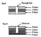
- through-holes are formed, if necessary.
- circuits are formed on both surfaces of the film, through-holes for connecting the circuits on both surfaces are usually formed.
- blind vias may be formed from the side of the roughenable cured resin layer.
- a method using a drill or a laser is mentioned.
- a laser is preferably used.
- the laser include a carbon dioxide gas laser, a UV-YAG laser, an excimer laser and the like.
- a UV-YAG laser is preferable.
- Examples of the oxidizing agent used to roughen the cured product surface and the inner wall of the through-hole or the blind via include an alkali permanganate solution, and solutions of oxidizing agents such as a bichromate, hydrogen peroxide, sulfuric acid and nitric acid. Especially, an alkali permanganate solution is preferable.
- Examples of the alkali permanganate solution can include a solution obtained by dissolving potassium permanganate or sodium permanganate in a sodium hydroxide aqueous solution.
- a conductor layer is formed on the roughened surface of the insulation layer (roughenable cured resin layer) and on the inner wall of the through-hole or the via hole by plating, and a circuit is formed on the surface of the insulation layer to form a circuit board, namely, a method of forming a circuit board using the film for a circuit board in the invention is described.
- the surface of the roughenable cured resin layer is roughened with the oxidizing agent such as the alkali permanganate solution to form a roughened anchor.
- a conductor layer is formed by a method which is a combination of electroless plating and electroplating. Further, it is also possible that a plating resist having a pattern opposite to that of the conductor layer is formed and the conductor layer is formed by electroless plating alone. Incidentally, adhesion strength of the conductor layer can be improved and stabilized by annealing at from 150 to 200°C for from 20 to 90 minutes after formation of the conductor layer.
- the through-holes or blind vias can usually be filled with the conductor simultaneously with the formation of the conductor layer on the surface of the insulation layer by the plating step.
- a method of forming a circuit by pattern-processing the conductor layer for example, a subtractive method and a semi-additive method which are known to a skilled person are available.
- a thickness of a electroless copper-plated layer is from 0.1 to 3 ⁇ m, preferably from 0.3 to 2.0 ⁇ m.
- a copper-electroplated layer (panel plated layer) is formed thereon with a thickness of from 3 to 35 ⁇ m, preferably from 5 to 20 ⁇ m, and an etching resist is then formed. Etching is performedwith an etching solution of ferric chloride, cupric chloride or the like to form a conductor pattern. Thereafter, the etching resist is removed thereby to obtain a circuit board.
- a electroless copper-plated layer is formed with a thickness of from 0.1 to 3 ⁇ m, preferably from 0.3 to 2.0 ⁇ m, and a pattern resist is then applied thereto to form a copper-electroplated layer (pattern plated layer) having a predetermined thickness (for example, from 9 to 18 ⁇ m). Thereafter, the pattern resist is removed to obtain a circuit board.
- the semi-additive method is appropriate for fine circuit formation.
- layer structure examples 1 to 8 are examples in which the roughenable cured resin layers (B layers) are formed on both surfaces of the heat-resistant resin layer (A layer). Even when the roughening resin composition layers are formed on both surfaces of the heat-resistant resin layer, a conductor layer can be formed only on one surface. Incidentally, the roughenable cured resin layer (B layer) can be formed only on one surface. However, since warpage of the film tends to increase in forming the cured product layer, it is undesirable.
- the roughenable cured resin layer is formed only on one surface of the heat-resistant resin layer, the cured resin layer (E layer) is formed on the remaining surface, and a copper foil is adhered to form a conductor layer.
- the invention is optionally used in combination with the prior technique.
- the resin composition used to form E layer is not required to be a resin composition capable of roughening in which the roughening component is incorporated as in B layer.
- B layer can be used also as E layer.
- thermosetting resin composition containing component (a) and component (b) and also known thermosetting compositions
- the copper foil (F layer) is not particularly limited, and those ordinarily used can be used.
- a copper foil having a thickness of from 3 to 18 ⁇ m is available.
- part(s) means part(s) by weight.
- thermosetting resin composition As thermosetting resin composition, This varnish type thermosetting resin composition was coated on a release-treated surface of a polyethylene naphthalate film having a thickness of 38 ⁇ m, and dried at from 80 to 120°C (on average 100°C)(residual amount of the solvent 2% by weight) to form a thermosetting resin composition layer having a film thickness of 10 ⁇ m. This layer was wound up in the form of a roll.
- thermosetting resin compositions having the thickness of 10 ⁇ m were adhered to both surfaces of a 25 ⁇ m thick polyimide film "Kapton EN" at the same time (both surfaces plasma-treated, manufactured by Du Pont-Toray Co., Ltd.) and the film was wound up in the form of a roll.
- the curing temperature was then raised from a low temperature to a high temperature. That is, the resulting product was cured at 120°C for 30 minutes and then at 170°C for 30 minutes.
- the layer structure of the resulting film for a (flexible) circuit board is polyethylene naphthalate film (peelable support film (C layer))/roughenable cured resin layer (B layer)/polyimide film (heat-resistant resin layer (A layer)/roughenable cured resin layer (B layer)/polyethylene naphthalate film (peelable support film (C layer)).
- thermosetting resin composition To the solution is added 4 parts of 2,4-diamino-6-(2-methyl-1-imidazolyl)ethyl-1,3,5-triazine as an epoxy curing agent. Further, 2 parts of pulverizing silica and 10 parts of calcium carbonate are added to form a resin varnish as thermosetting resin composition.
- the varnish type thermosetting resin composition is coated on a release-treated surface of a polyethylene terephthalate film having a thickness of 25 ⁇ m, and dried at from 80 to 120°C (on average 100°C) (residual amount of the solvent approximately 2% by weight) to forma thermosetting resin composition layer having a film thickness of 10 ⁇ m which is then wound up in the form of a roll.
- thermosetting resin composition having the thickness of 10 ⁇ m is adhered to one surface of a polyimide f ilm "Apical HP" (both surfaces corona-di scharged, manufactured by Kaneka Corporation) having a thickness of 12.5 ⁇ m, and the product is wound up in the form of a roll. This is cured at 120°C for 8 hours and then at 150°C for 4 hours.
- the layer structure of the resulting film for a (flexible) circuit board is polyethylene terephthalate film (peelable support film (C layer))/roughenable cured resin layer (B layer)/polyimide film (heat-resistant resin layer (A layer)).
- the polyethylene naphthalate film (peelable support film layer) was peeled from the film obtained in Example 1 to expose the roughenable cured resin layer.
- This layer was dipped in a swelling solution "Swelling Dip Securiganth P" (manufactured by Atotech Japan K. K.) at 80°C for 5 minutes to swell the surface of the roughenable cured resin layer which was then roughened by being dipped in an alkali manganate solution at 80°C for 10 minutes. Thereafter, manganese remaining on the surface of the roughenable cured resin layer was reductively removed.
- the layer structure of the resulting film for a (flexible) circuit board is electroless copper-plated layer (D1 layer)/roughenable cured resin layer (B layer)/polyimide film (heat-resistant resin layer (A layer)/roughenable cured resin layer (B layer)/electroless copper-plated layer (D1 layer).
- the layer structure of the resulting film for a (flexible) circuit board is copper-electroplated layer (D2 layer)/electroless copper-plated layer (D1 layer)/roughenable cured resin layer (B layer)/polyimide film (heat-resistant layer (A layer))/roughenable cured resin layer (B layer)/electroless copper-plated layer (D1 layer)/copper-electroplated layer (D2 layer).
- the adhesion strength of the plated coat was 0. 7 kg/cm.
- the polyethylene naphthalate film (peelable support film layer) is peeled from the film obtained in Example 2 to expose the roughenable cured resin layer.
- This layer is dipped in a swelling agent "Swelling Dip Securiganth P" (manufactured by Atotech Japan K.K.) at 80°C for 5 minutes to swell the surface of the roughenable cured resin layer which is then roughened by being dipped in an alkali manganate solution at 80°C for 10 minutes. Thereafter, manganese remaining on the surface of the roughenable cured resin layer is reductively removed.
- a catalyst for electroless copper plating is applied, and the resulting product is dipped in an electroless copper-plating solution at 32°C for 15 minutes to form an electroless copper-plated coat of 0.8 ⁇ m which is then dried at 120°C for 30 minutes.
- the layer structure of the resulting film for a (flexible) circuit board is electroless copper-plated layer (D1 layer)/roughenable cured resin layer (B layer)/polyimide film (heat-resistant resin layer (A layer)).
- electroplating with copper is performed at a cathode current density of 2.0 A/dm 2 for 20 minutes using a phosphorus-containing copper plate as an anode to form a copper-plated coat having a thickness of 8 ⁇ m, and the film is annealed at 170°C for 60 minutes.
- the layer structure of the resulting film for a (flexible) circuit board is copper-electroplated layer (D2 layer)/electroless copper-plated layer (D1 layer)/roughenable cured resin layer (B layer)/polyimide film (heat-resistant layer (A layer)).
- the polyethylene naphthalate film (peelable support film layer) was peeled from the film obtained in Example 1 to expose the roughenable cured resin layer. After via holes having a diameter of 30 ⁇ m were formed with UV-YAG laser, this layer was dipped in a swelling solution "Swelling Dip Securiganth P" (manufactured by Atotech Japan K.K.) at 80°C for 5 minutes to swell the surface of the roughenable cured resin layer which was then roughened by being dipped in an alkali manganate solution at 80°C for 10 minutes. Thereafter, manganese remaining on the surface of the roughenable cured resin layer was reductively removed.
- a swelling solution "Swelling Dip Securiganth P" (manufactured by Atotech Japan K.K.) at 80°C for 5 minutes to swell the surface of the roughenable cured resin layer which was then roughened by being dipped in an alkali manganate solution at 80°C for 10
- the layer structure of the resulting film for a (flexible) circuit board is electroless copper-plated layer (D1 layer)/roughenable cured resin layer (B layer)/polyimide film (heat-resistant resin layer (A layer))/roughenable cured resin layer (B layer)/electroless copper-plated layer (D1 layer).
- electroplating with copper was performed at a cathode current density of 2. 0 A/dm 2 for 12 minutes using a phosphorus-containing copper plate as an anode to form a copper-plated coat having a thickness of 5 ⁇ m, and the film was annealed at 170°C for 60 minutes.
- the layer structure of the resulting film for a (flexible) circuit board is copper-electroplated layer (D2 layer)/electroless copper-plated layer (D1 layer)/roughenable cured resin layer (B layer)/polyimide film (heat-resistant layer (A layer))/roughenable cured resin layer (B layer)/electroless copper-plated layer (D1 layer)/copper-electroplated layer (D2 layer).
- the adhesion strength of the plated coat was 0. 7 kg/cm.
- thermosetting resin varnish as in Example 1 was used as thermosetting resin composition, coating on a mat surface of a copper foil having a thickness of 18 ⁇ m, and dried at from 80 to 120°C (on average 100°C) (residual amount of the solvent 1.8% by weight) to form a thermosetting resin composition layer at a film thickness of 10 ⁇ m, and an aramid film "Aramica" (both surfaces plasma-treated, manufactured by Asahi Kasei Corporation) having a thickness of 4.5 ⁇ m was laminated on the thermosetting resin composition layer. The laminate was then wound up in the form of a roll. At this time, the layer structure of the film is aramid film (heat-resistant resin layer (A layer))/cured resin layer (E layer)/copper foil (F layer).
- thermosetting resin composition the same resin varnish as in Example 1 was used as thermosetting resin composition, and coated on a release-treated surface of a polyethylene terephthalate film having a thickness of 38 ⁇ m.
- the resulting product was dried at from 80 to 120°C (on average 100°C)(residual amount of the solvent 2.0 % by weight) to form a thermosetting resin composition layer at a film thickness of 10 ⁇ m.
- the aramid film surface of the film having the layer structure of aramid film (heat-resistant resin layer (A layer))/cured resin layer (E layer)/copper foil (F layer) produced previously as mentioned above was laminated on this thermosetting resin composition layer, and the laminate was wound up in the form of a roll.
- the curing temperature was raised from a low temperature to a high temperature, that is, the product was cured at 100°C for 2 hours and then at 150°C for 1 hour.
- the layer structure of the resulting film for a (flexible) circuit board is polyethylene terephthalate film (peelable support film (C layer))/roughenable cured resin layer (B layer)/aramid film (heat-resistant resin layer (A layer))/cured resin layer (E layer)/copper foil (F layer).
- thermosetting resin composition in the roughenable cured resin layer (B layer) and the cured resin layer (E layer).
- the polyethylene naphthalate film (peelable support film layer) was peeled from the film obtained in Example 6 to expose the roughenable cured resin layer. After blind via holes having a diameter of 25 ⁇ m were formed with UV-YAG laser, this layer was dipped in a swelling solution "Swelling Dip Securiganth P" (manufactured by Atotech Japan K.K.) at 60°C for 5 minutes to swell the surface of the roughenable cured resin layer which was then roughened by being dipped in an alkali manganate solution at 80°C for 10 minutes. Thereafter, manganese remaining on the surface of the roughenable cured resin layer was reductively removed.
- a swelling solution "Swelling Dip Securiganth P" (manufactured by Atotech Japan K.K.) at 60°C for 5 minutes to swell the surface of the roughenable cured resin layer which was then roughened by being dipped in an alkali manganate solution at 80°C for
- the layer structure of the resulting film for a (flexible) circuit board is electroless copper-plated layer (D1 layer)/roughenable cured resin layer (B layer)/aramid film (heat-resistant resin layer (A layer))/cured resin layer (E layer)/copper foil (F layer).
- electroplating with copper was performed at a cathode current density of 2.0 A/dm 2 for 30 minutes using a phosphorus-containing copper plate as an anode to form a copper-plated coat having a thickness of 12 ⁇ m, and the film was annealed at 170°C for 60 minutes.
- the layer structure of the resulting film for a (flexible) circuit board is copper-electroplated layer (D2 layer)/electroless copper-plated layer (D1 layer)/roughenable cured resin layer (B layer)/aramid film (heat-resistant layer (A layer))/cured resin layer (E layer)/copper foil (F layer).
- the adhesion strength of the plated coat was 0.75 kg/cm.
- the adhesion strength of a plated coat of commercially available "S'PERFLEX” (manufactured by Sumitomo Metal Mining Co., Ltd.) obtained by forming an Ni seed layer on a polyimide film "Kapton EN" of 25 ⁇ m through sputtering and conducting copper plating (8 ⁇ m) was 0.5 kg/cm.
- a circuit board capable of forming a fine pattern by plating and having high adhesion strength can easily be produced using the film for a (flexible) circuit board in the invention.
Landscapes
- Engineering & Computer Science (AREA)
- Microelectronics & Electronic Packaging (AREA)
- Manufacturing & Machinery (AREA)
- Laminated Bodies (AREA)
- Manufacturing Of Printed Wiring (AREA)
Abstract
A film for a circuit board characterized in that the
following A layer is adjacent to the following B layer is disclosed
in the present application. A circuit board excellent in
adhesion strength of a conductor layer can easily be produced
by using this film.
Description
The present invention relates to a film for a circuit board,
especially a film for a circuit board which can be utilized in
an electronic circuit and the like of portable devices such as
a cellular phone, PDA (personal digital assistant), a notebook
personal computer and the like, particularly a film suitable
for a flexible circuit board.
Polyimide resin films, liquid crystal polymer films,
aramid resin films, polyether ether ketone films and the like
have found wide acceptance as insulation materials of electronic
devices and the like because they are excellent in heat
resistance, dimensional stability, solvent resistance and
electrical and mechanical properties. Especially, a product
in which a conductor layer is formed on a polyimide resin film
has often been used in the flexible printedcircuit boards (FPC)
of tape automated bonding (TAB) or the like.
With respect to a method in which a conductor layer is
formed on a polyimide resin film, a laminating method in which
a polyimide resin film and a copper foil are adhered with an
adhesive (thermosetting resin composition) has, so far, been
mainstream. However, in a film for a board with a copper foil
which is produced by this method, the hole formation step in forming
a circuit is complicated. For example, when through-hole
formation for connecting circuits formed on both surfaces of
a film for a board is performed with a laser, it is required
that a step of hole formation of copper foils on both surfaces
through etching is first conducted and an insulation layer
portion is then drilled with a laser. Further, in the laminating
method, a copper foil having a certain thickness of, for example,
35 µm, 18 µm or 12 µm is used. There are problems that as the
thickness is increased, formation of a fine circuit by a
subtractive method is difficult, whereas when the thickness is
decreased, the cost is increased. Especially, when an inner
wall of a through-hole is plated, the thickness is increased
by plating a copper foil as well which is disadvantageous for
formation of a fine circuit.
In order to solve these problems, a method in which a
metallic layer as a base is directly formed on a polyimide resin
film by a dry process such as sputtering or deposition and a
conductor layer is then formed by electroless copper plating
and further by electroplating copper (JP-A-2001-77493 and
JP-A-9-136378) and a method in which a polyimide resin film is
directly plated to form a conductor layer (JP-A-8-31881 and
JP-A-7-243049) have been attempted. The former requires
formation of a metallic layer of cobalt, nickel or chromium as
a base by a dry metalizing method such as sputtering or vacuum
deposition for improving adhesion between the polyimide resin
film and the conductor layer. Thus, the step is complicated
and it is difficult to prevent generation of pinholes. Further,
the latter also requires a step of electroless nickel plating
or the like prior to electroless copper plating or electroplating
copper step in addition to special hydrophilic treatment on the
surface of the polyimide resin film. Thus, the step is
complicated, and adhesion strength is not necessarily at a
satisfactory level.
The invention aims to provide a film for producing simply
a circuit board excellent in adhesion strength of a conductor
layer, and further a film for a circuit board appropriate for
formation of a fine printed circuit.
The present inventors have assiduously conducted
investigations for solving the foregoing problems, and have
consequently found that a circuit board with a conductor layer
excellent in adhesion can easily be produced from a film in which
a specific roughenable cured resin layer is formed on a
heat-resistant resin layer of a specific polyimide resin, liquid
crystal polymer or the like through a general-purpose process
of roughening, electroless copper plating and electroplating
copper, and further that the film becomes a film suitable for
a circuit board that allows formation of a fine printed circuit.
, The invention has been completed on the basis of such findings.
That is, the invention relates to a film for a circuit
board characterized in that the following A layer is adjacent
to the following B layer.
The invention is described in detail below.
The film for a circuit board in the invention has "a
heat-resistant resin layer with a thickness of from 2 to 250
µm which layer is made of a heat-resistant resin having a glass
transition point of 200°C or more or a decomposition temperature
of 300°C or more" (which is sometimes abbreviated as "A layer"
or "heat-resistant resin layer" in the present specification).
The heat-resistant resin used in the invention has a glass
transition point of 200°C or more or a decomposition temperature
of 300°C or more which satisfies heat resistance in soldering
required in the production of a multilayer printed wiring board.
Here, the decomposition temperature is defined in terms of a
temperature at which the weight reduction rate becomes 5% when
measured according to JIS (Japanese Industrial Standards) K 7120
(gravimetry of plastics).
The heat-resistant resin comprising the heat-resistant
resin layer is preferably selected from a polyimide resin, a
liquid crystal polymer, an aramid resin and a polyether ether
ketone. Especially, a polyimide resin is preferable.
Incidentally, as the liquid crystal polymer, a liquid crystal
polymer which is structurally a wholly aromatic polyester is
preferably used.
When the thickness of the heat-resistant resin layer is
less than 2 µm, mechanical strength of an insulation layer or
a multilayer printed wiring board might be insufficient. When
it exceeds 250 µm, the cost is increased, and the thickness of
the insulation layer becomes more than is required. Thus, these
are undesirable. As a layer for a flexible printed circuit board,
a layer having a thickness of from 2 to 75 µm is ordinarily used.
A layer having a thickness of from 75 to 250 µm is suitable for
use in, for example, an interposer of CSP (chip-size package).
In the heat-resistant resin layer in the film for a circuit
board of the invention, a heat-resistant resin marketed in the
form of a film can be used. For example, heat-resistant resin
films such as a polyimide film "Upilex-S" manufactured by Ube
Industries, Ltd., a polyimide film "Kapton" manufactured by Du
Pont-Toray Co., Ltd., a polyimide film "Apical" manufactured
by Kaneka Corporation, an aramid film "Aramica" manufactured
by Asahi Kasei Corporation, anaramid film "Mictron" manufactured
by Toray Industries Inc., a liquid crystal polymer film "Vecstar"
manufactured by Kuraray Co. , Ltd. and a polyether ether ketone
film "Sumilite FS-1100C" manufactured by Sumitomo Bakelite Co.,
Ltd. are available.
As the heat-resistant resin layer (A layer), a
surface-treated layer may be used. Examples of the surface
treatment include dry treatments such as corona discharge, plasma
treatment and ion beam treatment, chemical treatments with a
solvent, an acid and an alkali, mechanical polishing and the
like. Especially in view of adhesion with B layer, it is
preferable to apply plasma treatment.
The film for a circuit board in the invention has also
"a roughenable cured resin layer with a thickness of from 5 to
20 µm which layer is made of a cured product of a thermosetting
resin composition containing at least component (a) of an epoxy
resin having two or more epoxy groups in a molecule and component
(b) of an epoxy curing agent, the cured product being capable
of roughening with an oxidizing agent" (which is sometimes
abbreviated as B layer or "roughenable cured resin layer" in
the present specification). This is described below.
As the "epoxy resin having two or more epoxy groups in
a molecule" as component (a), an aromatic epoxy resin having
an aromatic ring structure in a molecule is preferably used for
increasing the heat resistance. Examples thereof can include
epoxy resins having two or more epoxy groups in a molecule, such
as a bisphenol A-type epoxy resin, a bisphenol F-type epoxy resin,
a phenolic novolak-type epoxy resin, a bisphenol S-type epoxy
resin, an alkylphenolic novolak-type epoxy resin, a
biphenol-type epoxy resin, a naphthalene-type epoxy resin, an
epoxy compound of a condensate of a phenol and an aromatic aldehyde
having a phenolic hydroxyl group, and the like. Further, the
epoxy resin may be brominated or the like for imparting fire
retardance.
Examples of the "epoxy curing agent" as component (b) can
include an amine-type curing agent, a guanidine-type curing
agent, an imidazole-type curing agent, a phenolic curing agent,
an acid anhydride-type curing agent, epoxy adducts or
microcapsules thereof, and the like. Further, with respect to
the curing agents, those having a longer pot life are preferable.
Two or more of the epoxy curing agents can also be used in
combination.
Specific examples of the epoxy curing agents can include
dicyandiamide, 2-phenyl-4-methyl-5-hydroxymethylimidazole,
2-phenyl-4,5-bis(hydroxymethyl)imidazole,
2,4-diamino-6-(2-methyl-1-imidazolylethyl)-1,3,5-triazine
isocyanuric acid adduct,
2,4-diamino-6-(2-undecyl-1-imidazolylethyl)-1,3,5-triazine
and the like.
As the epoxy curing agent, the phenolic curing agent having
a nitrogen atom is especially preferable. The use of the phenolic
curing agent having the nitrogen atom is effective for improving
heat resistance, fire retardance and adhesion of the insulation
layer. Examples of such an epoxy curing agent can include a
triazine structure-containing novolak resin (for example,
"Phenolite 7050 Series" manufactured by Dainippon Ink and
Chemicals, Inc.) and a melamine-modified phenolic novolak resin
(for example, "YLH 828" manufactured by Japan Epoxy Resins Co.,
Ltd.).
These epoxy curing agents in the thermosetting resin
composition can ordinarily be used in the range of from 2 to
12% by weight in case of the amine-type curing agent,
guanidine-type curing agent and imidazole-type curing agent,
and ordinarily in the range of from 0.5 to 1.3 equivalents per
equivalent of the epoxy group of the epoxy resin contained in
the thermosetting resin composition in terms of a phenolic
hydroxyl group equivalent or an acid anhydride equivalent.
Besides the epoxy curing agent, a curing accelerator can
also be added. Examples of the curing accelerator include an
imidazole-type compound, an organic phosphine-type compound and
the like. In case of using the curing accelerator, it can
preferably be used in the range of from 0.5 to 2% by weight based
on the epoxy resin contained in the thermosetting resin
composition.
As the thermosetting resin composition which is a material
of the roughenable cured resin layer in the film for a circuit
board in the invention, it is preferable to use a composition
having a glass transition point of 150°C or more. This can easily
be prepared by a skilled person upon using, for example, an
aromatic epoxy resin having an aromatic ring structure in a
molecule (a) or upon further using a phenolic curing agent having
a nitrogen atom as component (b).
In the thermosetting resin composition in the invention,
the surface of the cured product can be roughened with an oxidizing
agent after heat curing. A conductor layer excellent in peel
strength can easily be formed by roughening and plating the
surface of the cured product.
In order to be able to roughen the surface of the thus-cured
resin composition, a roughening component may be contained in
the thermosetting resin composition. When the thermosetting
resin composition in the invention uses a phenolic curing agent
as an epoxy curing agent (component (b)) and contains a phenoxy
resin having a bisphenol S structure and a weight average
molecular weight of from 5,000 to 100,000, roughening with an
oxidizing agent is possible without containing a roughening
component in particular.
Examples of the roughening component can include a rubber
component, an amino resin, an inorganic filler, an organic filler
and the like.
Examples of the rubber component can include a
polybutadiene rubber, an epoxy-modified polybutadiene rubber,
a urethane-modified polybutadiene rubber, an
acrylonitrile-modified polybutadiene rubber, a
methacrylonitrile-modified polybutadiene rubber, a carboxyl
group-containing acrylonitrile·butadiene rubber, a carboxyl
group-containing methacrylonitrile·butadiene rubber, an
acrylic rubber-dispersed epoxy resin and the like.
Examples of the amino resin can include amino resins such
as a melamine resin, a guanamine resin and a urea resin, these
amino acids which are alkyl-etherified, and the like.
Examples of the inorganic filler include calcium carbonate,
magnesium carbonate, magnesium oxide, aluminum hydroxide and
the like.
And, examples of the organic filler can include an epoxy
resin powder, a crosslinked acrylic polymer, the foregoing amino
resins which are heat-cured and pulverized, and the like.
When the thermosetting resin composition according to the
invention contains the roughening component, the proportion of
the roughening component is preferably from 5 to 40% by weight,
more preferably from 10 to 30% by weight. When it is less than
5% by weight, the roughening might be insufficient. Meanwhile,
when it exceeds 40% by weight, the insulating property, chemical
resistance and heat resistance of the insulation layer after
curing tend to decrease.
Examples of a phenoxy resin having a weight average
molecular weight of from 5,000 to 100,000 can include phenoxy
resins such as "Phenotohto YP50" (manufactured by Tohto Kasei
Co., Ltd.) and "E-1256" (manufactured by Japan Epoxy Resins Co.,
Ltd.), and brominated phenoxy resins such as "YPB-40-PXM40"
(manufactured by Tohto Kasei Co., Ltd.). Further, examples of
a phenoxy resin with a bisphenol S structure having a weight
average molecular weight of from 5,000 to 10,000 can include
"YL6747H30" (manufactured by Japan Epoxy Resins Co., Ltd., a
cyclohexanone varnish of a phenoxy resin made of a bisphenol
A-type epoxy resin "Epikote 828" and bisphenol S: nonvolatile
component 30% by weight, weight average molecular weight 47,000),
"YL6746H30" (manufactured by Japan Epoxy Resins Co., Ltd., a
cyclohexanone varnish of a phenoxy resin made of a bixylenol-type
epoxy resin "Epikote YX4000" and bisphenol S: nonvolatile content
30% by weight, weight average molecular weight 40,000), and the
like. It is preferable that such a phenoxy resin is contained
in the thermosetting resin composition in an amount of from 5
to 50% by weight.
The thermosetting resin composition can also contain an
inorganic filler other than the inorganic filler used as the
roughening component for imparting various functions. Examples
of the inorganic filler used as the additive can include barium
sulfate, barium titanate, silicon oxide powder, amorphous
silica, talc, clay, mica powder and the like. These inorganic
fillers other than the roughening component can be used in the
thermosetting resin composition in the range of from 10 to 80%
by weight.
Further, the thermosetting resin composition of the
invention can contain other various resin additives which are
used in this field, if necessary. Examples of such additives
can include a thickening agent, a defoamer, a leveling agent,
an adhesion-imparting agent, a colorant, a flame retardant
adjuvant, an inorganic filler, an organic filler and the like.
With respect to a method of forming the roughenable cured
resin layer (B layer), for example, a resin varnish in which
the thermosetting resin composition already described has been
dissolved in an appropriate organic solvent is prepared, and
this resin varnish is coated on a peelable support film layer
(C layer) as a support. The organic solvent is dried by heating,
hot air blowing or the like to first form a thermosetting resin
composition layer. The thermosetting resin composition of the
film comprising the peelable support film layer (C layer) and
the thermosetting resin composition layer is adhered to both
surfaces or one surface of the heat-resistant film layer (A
layer). The resulting film is heated to heat-cure the
thermosetting resin composition layer and form the roughenable
cured resin layer (B layer). The curing conditions vary with
the components of the thermosetting resin composition. The
curing temperature is usually selected from the range of from
100 to 200°C, and the curing temperature from the range of from
10 minutes to 15 hours. The curing which is performed by raising
the temperature from a relatively low curing temperature to a
high curing temperature is preferable to the curing which is
not performed in this manner, in view of preventing occurrence
of wrinkles or voids on the surface of the roughenable cured
resin layer formed.
The thickness of B layer is from 5 to 20 µm, preferably
from 7 to 15 µm. When the thickness of B layer is less than
5 µm, satisfactory formation of a roughened surface is difficult.
Meanwhile, when it exceeds 20 µm, flexibility in using the layer
in a flexible printed circuit board might be insufficient,
warpage of a cured product layer in curing the resin composition
might be increased, or a hole formation step might be difficult.
Examples of the organic solvent used in preparing the resin
varnish of the thermosetting resin composition can include
ketones such as acetone, methyl ethyl ketone and cyclohexanone,
acetate esters such as ethyl acetate, butyl acetate, cellosolve
acetate, propylene glycol monomethyl ether acetate and carbitol
acetate, cellosolves such as cellosolve and butyl cellosolve,
carbitols such as carbitol and butyl carbitol, aromatic
hydrocarbons such as toluene and xylene, amides such as
dimethylformamide, dimethylacetamide and N-methylpyrrolidone,
and the like. Two or more of these organic solvents can also
be used in combination.
The peelable support film in the invention plays a part
of support material when forming the roughenable cured resin
layer from the thermosetting resin composition, and also plays
a part of preventing adhesion of a contaminant or the like to
the roughenable cured resin layer in the heat curing.
As the peelable film used as the peelable support film
layer (C layer), films of polyesters such as polyethylene
terephthalate and polyethylene naphthalate, polycarbonates, a
release paper and the like can be used. The thickness of the
peelable support film is generally from 10 to 150 µm, preferably
from 25 to 50 µm. Incidentally, the peelable support film may
be subjected to mat treatment, corona treatment, release
treatment or the like.
The peelable support film in the invention is preferably
peeled after heat-curing the thermosetting resin composition
to form the roughenable cured resin layer. The peelable support
film is usually subjected to release treatment in advance.
After peeling the peelable support film, through-holes
are formed, if necessary. When circuits are formed on both
surfaces of the film, through-holes for connecting the circuits
on both surfaces are usually formed. By the way, in case of
a layer structure in which a copper foil is provided on one surface
of the heat-resistant resin layer, blind vias may be formed from
the side of the roughenable cured resin layer.
As a method of forming through-holes and blind vias, a
method using a drill or a laser is mentioned. In view of forming
holes having a smaller diameter, a laser is preferably used.
Examples of the laser include a carbon dioxide gas laser, a UV-YAG
laser, an excimer laser and the like. Especially, in case of
a hole having a small diameter of less than 50 µm, a UV-YAG laser
is preferable.
Examples of the oxidizing agent used to roughen the cured
product surface and the inner wall of the through-hole or the
blind via include an alkali permanganate solution, and solutions
of oxidizing agents such as a bichromate, hydrogen peroxide,
sulfuric acid and nitric acid. Especially, an alkali
permanganate solution is preferable. Examples of the alkali
permanganate solution can include a solution obtained by
dissolving potassium permanganate or sodium permanganate in a
sodium hydroxide aqueous solution.
Next, a method in which a conductor layer is formed on
the roughened surface of the insulation layer (roughenable cured
resin layer) and on the inner wall of the through-hole or the via
hole by plating, and a circuit is formed on the surface of
the insulation layer to form a circuit board, namely, a method
of forming a circuit board using the film for a circuit board
in the invention is described.
First, the surface of the roughenable cured resin layer
is roughened with the oxidizing agent such as the alkali
permanganate solution to form a roughened anchor.
Subsequently, a conductor layer is formed by a method which is
a combination of electroless plating and electroplating.
Further, it is also possible that a plating resist having a pattern
opposite to that of the conductor layer is formed and the conductor
layer is formed by electroless plating alone. Incidentally,
adhesion strength of the conductor layer can be improved and
stabilized by annealing at from 150 to 200°C for from 20 to 90
minutes after formation of the conductor layer. When the film
for a circuit board in the invention has through-holes or blind
vias having a diameter of, for example, less than 50 µm, the
through-holes or blind vias can usually be filled with the
conductor simultaneously with the formation of the conductor
layer on the surface of the insulation layer by the plating step.
As a method of forming a circuit by pattern-processing
the conductor layer, for example, a subtractive method and a
semi-additive method which are known to a skilled person are
available.
In case of the subtractive method, a thickness of a
electroless copper-plated layer is from 0.1 to 3 µm, preferably
from 0.3 to 2.0 µm. A copper-electroplated layer (panel plated
layer) is formed thereon with a thickness of from 3 to 35 µm,
preferably from 5 to 20 µm, and an etching resist is then formed.
Etching is performedwith an etching solution of ferric chloride,
cupric chloride or the like to form a conductor pattern.
Thereafter, the etching resist is removed thereby to obtain
a circuit board. Further, in case of the semi-additive method,
a electroless copper-plated layer is formed with a thickness
of from 0.1 to 3 µm, preferably from 0.3 to 2.0 µm, and a pattern
resist is then applied thereto to form a copper-electroplated
layer (pattern plated layer) having a predetermined thickness
(for example, from 9 to 18 µm). Thereafter, the pattern resist
is removed to obtain a circuit board. Especially,
the semi-additive method is appropriate for fine circuit
formation.
As the preferable layer structure of the film for a circuit
board according to the invention, for example, the following
layer structure examples 1 to 8 can be listed. Of these layer
structure examples, layer structure examples 1 to 4 are examples
in which the roughenable cured resin layers (B layers) are formed
on both surfaces of the heat-resistant resin layer (A layer).
Even when the roughening resin composition layers are formed
on both surfaces of the heat-resistant resin layer, a conductor
layer can be formed only on one surface. Incidentally, the
roughenable cured resin layer (B layer) can be formed only on
one surface. However, since warpage of the film tends to increase
in forming the cured product layer, it is undesirable.
Moreover, as shown in layer structure examples 5 to 8,
the roughenable cured resin layer is formed only on one surface
of the heat-resistant resin layer, the cured resin layer (E layer)
is formed on the remaining surface, and a copper foil is adhered
to form a conductor layer. In this manner, the invention is
optionally used in combination with the prior technique. Here,
there is no need to roughen the cured resin layer (E layer).
Accordingly, the resin composition used to form E layer is not
required to be a resin composition capable of roughening in which
the roughening component is incorporated as in B layer. However,
B layer can be used also as E layer. As the resin composition
used to form F layer, the foregoing thermosetting resin
composition containing component (a) and component (b) and also
known thermosetting compositions can be used. The copper foil
(F layer) is not particularly limited, and those ordinarily used
can be used. For example, a copper foil having a thickness of
from 3 to 18 µm is available.
roughenable cured resin layer (B layer)/heat-resistant resin layer (A layer)/roughenable cured resin layer (B layer),
peelable support film layer (C layer)/roughenable cured resin layer (B layer)/heat-resistant resin layer (A layer)/roughenable cured resin layer (B layer)/peelable support film layer (C layer),
electroless copper-plated layer (D1 layer)/roughenable cured resin layer (B layer)/heat-resistant resin layer (A layer)/roughenable cured resin layer (B layer)/electroless copper-plated layer (D1 layer),
copper-electroplated layer (D2 layer)/electroless copper-plated layer (D1 layer)/roughenable cured resin layer (B layer)/heat-resistant resin layer (A layer)/roughenable cured resin layer (B layer)/electroless copper-plated layer (D1 layer)/copper-electroplated layer (D2 layer),
The invention is illustrated specifically below by
referring to Examples. However, the invention is not limited
by these Examples. Incidentally, in Examples, part(s) means
part(s) by weight.
20 parts of a bisphenol A-type epoxy resin "Epikote 828"
(epoxy equivalent 190, manufactured by Japan Epoxy Resins Co.,
Ltd.) and 35 parts of a cresol novolak-type epoxy resin "Epiclon N-673"
(epoxy equivalent 215, softening point 78°C, manufactured by
Dainippon Ink and Chemicals, Inc.) were heat-dissolved in
2-butanone while being stirred, and the solution was then cooled
to room temperature. Subsequently, 45 parts of a 2-butanone
solution of a triazine structure-containing phenolic novolak
resin, "Phenolite LA-7052 (nonvolatile content 60%, nonvolatile
content phenolic hydroxyl group equivalent 120, manufactured
by Dainippon Ink and Chemicals, Inc.), 70 parts of a cyclohexanone
solution of a phenoxy resin "YL-6746H30" (nonvolatile content
30% by weight, weight average molecular weight 30,000,
manufactured by Japan Epoxy Resins Co., Ltd.) comprising a
bixylenol-type epoxy resin "Epikote YX-4000" (epoxy equivalent
185, manufactured by Japan Epoxy Resins Co. , Ltd.) and bisphenol
S, further 18 parts of spherical silica and 2 parts of pulverizing
silica were added to prepare a resin varnish as thermosetting
resin composition. This varnish type thermosetting resin
composition was coated on a release-treated surface of a
polyethylene naphthalate film having a thickness of 38 µm, and
dried at from 80 to 120°C (on average 100°C)(residual amount
of the solvent 2% by weight) to form a thermosetting resin
composition layer having a film thickness of 10 µm. This layer
was wound up in the form of a roll.
Then, the surfaces of the thermosetting resin compositions
having the thickness of 10 µm were adhered to both surfaces of
a 25 µm thick polyimide film "Kapton EN" at the same time (both
surfaces plasma-treated, manufactured by Du Pont-Toray Co., Ltd.)
and the film was wound up in the form of a roll. The
curing temperature was then raised from a low temperature to
a high temperature. That is, the resulting product was cured
at 120°C for 30 minutes and then at 170°C for 30 minutes.
The layer structure of the resulting film for a (flexible)
circuit board is polyethylene naphthalate film (peelable support
film (C layer))/roughenable cured resin layer (B
layer)/polyimide film (heat-resistant resin layer (A
layer)/roughenable cured resin layer (B layer)/polyethylene
naphthalate film (peelable support film (C layer)).
50 parts of a brominated bisphenol-type epoxy resin
"YDB-500" (epoxy equivalent 500, manufactured by Tohto Kasei
Co., Ltd.), 20 parts of a cresol novolak-type epoxy resin "Epiclon
N-673" (epoxy equivalent 215, softening point 78°C, manufactured
by Dainippon Ink and Chemicals, Inc.) and 15 parts of a
terminal-epoxidized butadiene rubber "Denalex R-45 EPT"
(manufactured by Nagase Chemicals, Ltd.) are heat-dissolved in
a 2-butanone/toluene mixed solvent while being stirred. To the
solution is added 4 parts of 2,4-diamino-6-(2-methyl-1-imidazolyl)ethyl-1,3,5-triazine
as an epoxy curing agent.
Further, 2 parts of pulverizing silica and 10 parts of calcium
carbonate are added to form a resin varnish as thermosetting
resin composition. The varnish type thermosetting resin
composition is coated on a release-treated surface of a
polyethylene terephthalate film having a thickness of 25 µm,
and dried at from 80 to 120°C (on average 100°C) (residual amount
of the solvent approximately 2% by weight) to forma thermosetting
resin composition layer having a film thickness of 10 µm which
is then wound up in the form of a roll.
Subsequently, the surface of the thermosetting resin
composition having the thickness of 10 µm is adhered to one surface
of a polyimide f ilm "Apical HP" (both surfaces corona-di scharged,
manufactured by Kaneka Corporation) having a thickness of 12.5
µm, and the product is wound up in the form of a roll. This
is cured at 120°C for 8 hours and then at 150°C for 4 hours.
The layer structure of the resulting film for a (flexible)
circuit board is polyethylene terephthalate film (peelable
support film (C layer))/roughenable cured resin layer (B
layer)/polyimide film (heat-resistant resin layer (A layer)).
The polyethylene naphthalate film (peelable support film
layer) was peeled from the film obtained in Example 1 to expose
the roughenable cured resin layer. This layer was dipped in
a swelling solution "Swelling Dip Securiganth P" (manufactured
by Atotech Japan K. K.) at 80°C for 5 minutes to swell the surface
of the roughenable cured resin layer which was then roughened
by being dipped in an alkali manganate solution at 80°C for 10
minutes. Thereafter, manganese remaining on the surface of the
roughenable cured resin layer was reductively removed.
Subsequently, a catalyst for electroless copper plating
was applied, and the resulting product was then dipped in a
electroless copper-plating solution at 32°C for 30 minutes to
form an electroless copper-plated coat of 1.5 µm. The film was
dried at 120°C for 30 minutes.
The layer structure of the resulting film for a (flexible)
circuit board is electroless copper-plated layer (D1
layer)/roughenable cured resin layer (B layer)/polyimide film
(heat-resistant resin layer (A layer)/roughenable cured resin
layer (B layer)/electroless copper-plated layer (D1 layer).
After the resulting film was washed with an acid,
electroplating with copper was performed at a cathode current density
of 2.0 A/dm2 for 12 minutes using a phosphorus-containing copper
plate as an anode to form a copper-plated coat having a thickness
of 5 µm, and the film was annealed at 170°C for 60 minutes.
The layer structure of the resulting film for a (flexible)
circuit board is copper-electroplated layer (D2
layer)/electroless copper-plated layer (D1 layer)/roughenable
cured resin layer (B layer)/polyimide film (heat-resistant layer
(A layer))/roughenable cured resin layer (B layer)/electroless
copper-plated layer (D1 layer)/copper-electroplated layer (D2
layer). The adhesion strength of the plated coat was 0. 7 kg/cm.
The polyethylene naphthalate film (peelable support film
layer) is peeled from the film obtained in Example 2 to expose
the roughenable cured resin layer. This layer is dipped in a
swelling agent "Swelling Dip Securiganth P" (manufactured by
Atotech Japan K.K.) at 80°C for 5 minutes to swell the surface
of the roughenable cured resin layer which is then roughened
by being dipped in an alkali manganate solution at 80°C for 10
minutes. Thereafter, manganese remaining on the surface of the
roughenable cured resin layer is reductively removed.
Subsequently, a catalyst for electroless copper plating
is applied, and the resulting product is dipped in an electroless
copper-plating solution at 32°C for 15 minutes to form an
electroless copper-plated coat of 0.8 µm which is then dried
at 120°C for 30 minutes.
The layer structure of the resulting film for a (flexible)
circuit board is electroless copper-plated layer (D1
layer)/roughenable cured resin layer (B layer)/polyimide film
(heat-resistant resin layer (A layer)).
After the resulting film is washed with an acid,
electroplating with copper is performed at a cathode current density
of 2.0 A/dm2 for 20 minutes using a phosphorus-containing copper
plate as an anode to form a copper-plated coat having a thickness
of 8 µm, and the film is annealed at 170°C for 60 minutes.
The layer structure of the resulting film for a (flexible)
circuit board is copper-electroplated layer (D2
layer)/electroless copper-plated layer (D1 layer)/roughenable
cured resin layer (B layer)/polyimide film (heat-resistant layer
(A layer)).
The polyethylene naphthalate film (peelable support film
layer) was peeled from the film obtained in Example 1 to expose
the roughenable cured resin layer. After via holes having a
diameter of 30 µm were formed with UV-YAG laser, this layer was
dipped in a swelling solution "Swelling Dip Securiganth P"
(manufactured by Atotech Japan K.K.) at 80°C for 5 minutes to
swell the surface of the roughenable cured resin layer which
was then roughened by being dipped in an alkali manganate solution
at 80°C for 10 minutes. Thereafter, manganese remaining on the
surface of the roughenable cured resin layer was reductively
removed.
Subsequently, a catalyst for electroless copper plating
was applied, and the resulting product was then dipped in an
electroless copper-plating solution at 32°C for 30 minutes to
form an electroless copper-plated coat of 1. 5 µm which was then
dried at 120°C for 30 minutes.
The layer structure of the resulting film for a (flexible)
circuit board is electroless copper-plated layer (D1
layer)/roughenable cured resin layer (B layer)/polyimide film
(heat-resistant resin layer (A layer))/roughenable cured resin
layer (B layer)/electroless copper-plated layer (D1 layer).
After the resulting film was washed with an acid,
electroplating with copper was performed at a cathode current density
of 2. 0 A/dm2 for 12 minutes using a phosphorus-containing copper
plate as an anode to form a copper-plated coat having a thickness
of 5 µm, and the film was annealed at 170°C for 60 minutes.
The layer structure of the resulting film for a (flexible)
circuit board is copper-electroplated layer (D2
layer)/electroless copper-plated layer (D1 layer)/roughenable
cured resin layer (B layer)/polyimide film (heat-resistant layer
(A layer))/roughenable cured resin layer (B layer)/electroless
copper-plated layer (D1 layer)/copper-electroplated layer (D2
layer). The adhesion strength of the plated coat was 0. 7 kg/cm.
The'same resin varnish as in Example 1 was used as
thermosetting resin composition, coating on a mat surface
of a copper foil having a thickness of 18 µm, and dried at from
80 to 120°C (on average 100°C) (residual amount of the solvent
1.8% by weight) to form a thermosetting resin composition layer
at a film thickness of 10 µm, and an aramid film "Aramica" (both
surfaces plasma-treated, manufactured by Asahi Kasei
Corporation) having a thickness of 4.5 µm was laminated on the
thermosetting resin composition layer. The laminate was then
wound up in the form of a roll. At this time, the layer structure
of the film is aramid film (heat-resistant resin layer (A
layer))/cured resin layer (E layer)/copper foil (F layer).
Subsequently, the same resin varnish as in Example 1 was
used as thermosetting resin composition, and coated on a
release-treated surface of a polyethylene terephthalate film
having a thickness of 38 µm. The resulting product was dried
at from 80 to 120°C (on average 100°C)(residual amount of the
solvent 2.0 % by weight) to form a thermosetting resin composition
layer at a film thickness of 10 µm. The aramid film surface
of the film having the layer structure of aramid film
(heat-resistant resin layer (A layer))/cured resin layer (E
layer)/copper foil (F layer) produced previously as mentioned
above was laminated on this thermosetting resin composition
layer, and the laminate was wound up in the form of a roll. The
curing temperature was raised from a low temperature to a high
temperature, that is, the product was cured at 100°C for 2 hours
and then at 150°C for 1 hour.
The layer structure of the resulting film for a (flexible)
circuit board is polyethylene terephthalate film (peelable
support film (C layer))/roughenable cured resin layer (B
layer)/aramid film (heat-resistant resin layer (A layer))/cured
resin layer (E layer)/copper foil (F layer).
In this Example, the same resin varnish is used as
thermosetting resin composition in the roughenable cured
resin layer (B layer) and the cured resin layer (E layer).
The polyethylene naphthalate film (peelable support film
layer) was peeled from the film obtained in Example 6 to expose
the roughenable cured resin layer. After blind via holes having
a diameter of 25 µm were formed with UV-YAG laser, this layer
was dipped in a swelling solution "Swelling Dip Securiganth P"
(manufactured by Atotech Japan K.K.) at 60°C for 5 minutes to
swell the surface of the roughenable cured resin layer which
was then roughened by being dipped in an alkali manganate solution
at 80°C for 10 minutes. Thereafter, manganese remaining on the
surface of the roughenable cured resin layer was reductively
removed.
Subsequently, a catalyst for electroless copper plating
was applied, and the resulting product was then dipped in an
electroless copper-plating solution at 32°C for 30 minutes to
form an electroless copper-plated coat of 1.5 µm which was then
dried at 120°C for 30 minutes.
The layer structure of the resulting film for a (flexible)
circuit board is electroless copper-plated layer (D1
layer)/roughenable cured resin layer (B layer)/aramid film
(heat-resistant resin layer (A layer))/cured resin layer (E
layer)/copper foil (F layer).
After the resulting film was washed with an acid,
electroplating with copper was performed at a cathode current density
of 2.0 A/dm2 for 30 minutes using a phosphorus-containing copper
plate as an anode to form a copper-plated coat having a thickness
of 12 µm, and the film was annealed at 170°C for 60 minutes.
The layer structure of the resulting film for a (flexible)
circuit board is copper-electroplated layer (D2
layer)/electroless copper-plated layer (D1 layer)/roughenable
cured resin layer (B layer)/aramid film (heat-resistant layer
(A layer))/cured resin layer (E layer)/copper foil (F layer).
The adhesion strength of the plated coat was 0.75 kg/cm.
The adhesion strength of a plated coat of commercially
available "S'PERFLEX" (manufactured by Sumitomo Metal Mining
Co., Ltd.) obtained by forming an Ni seed layer on a polyimide
film "Kapton EN" of 25 µm through sputtering and conducting copper
plating (8 µm) was 0.5 kg/cm.
A circuit board capable of forming a fine pattern by plating
and having high adhesion strength can easily be produced using
the film for a (flexible) circuit board in the invention.
Claims (14)
- A film for a circuit board characterized in that the following A layer is adjacent to the following B layer.A layer: a heat-resistant resin layer with a thickness of from 2 to 250 µm which layer is made of a heat-resistant resin having a glass transition point of 200°C or more or a decomposition temperature of 300°C or more, andB layer: a roughenable cured resin layer with a thickness of from 5 to 20 µm which layer is made of a cured product of a thermosetting resin composition containing at least component (a) of an epoxy resin having two or more epoxy groups in a molecule and component (b) of an epoxy curing agent, the cured product being capable of roughening with an oxidizing agent.
- A film for a circuit board characterized in that the film comprises the following A layer, B layer and C layer, and has a layer structure of C layer, B layer and A layer in this order:A layer: a heat-resistant resin layer with a thickness of from 2 to 250 µm which layer is made of a heat-resistant resin having a glass transition point of 200°C or more or a decomposition temperature of 300°C or more,B layer: a roughenable cured resin layer with a thickness of from 5 to 20 µm which layer is made of a cured product of a thermosetting resin composition containing at least component (a) of an epoxy resin having two or more epoxy groups in a molecule and component (b) of an epoxy curing agent, the cured product being capable of roughening with an oxidizing agent, andC layer: a peelable support film.
- A film for a circuit board characterized in that the film comprises the following A layer, B layer and D layer, and has a layer structure of D layer, B layer and A layer in this order:A layer: a heat-resistant resin layer with a thickness of from 2 to 250 µm which layer is made of a heat-resistant resin having a glass transition point of 200°C or more or a decomposition temperature of 300°C or more,B layer: a roughenable cured resin layer with a thickness of from 5 to 20 µm which layer is made of a cured product of a thermosetting resin composition containing at least component (a) of an epoxy resin having two or more epoxy groups in a molecule and component (b) of an epoxy curing agent, the cured product being capable of roughening with an oxidizing agent, andD layer: a conductor layer.
- The film for a circuit board as claimed in claim 3, characterized in that the conductor layer is an electroless copper-plated layer (D1 layer).
- The film for a circuit board as claimed in claim 3, characterized in that the conductor layer comprises an electroless copper-plated layer (D1 layer) and a copper-electroplated layer (D2 layer).
- A film for a circuit board characterized in that the film comprises the following A layer, B layer and C layer, and has a layer structure of C layer, B layer, A layer, B layer and C layer in this order:A layer: a heat-resistant resin layer with a thickness of from 2 to 250 µm which layer is made of a heat-resistant resin having a glass transition point of 200°C or more or a decomposition temperature of 300°C or more,B layer: a roughenable cured resin layer with a thickness of from 5 to 20 µm which layer is made of a cured product of a thermosetting resin composition containing at least component (a) of an epoxy resin having two or more epoxy groups in a molecule and component (b) of an epoxy curing agent, the cured product being capable of roughening with an oxidizing agent, andC layer: a peelable support film.
- A film for a circuit board characterized in that the film comprises the following A layer, B layer and D layer and has a layer structure of D layer, B layer, A layer, B layer and D layer in this order:A layer: a heat-resistant resin layer with a thickness of from 2 to 250 µm which layer is made of a heat-resistant resin having a glass transition point of 200°C or more or a decomposition temperature of 300°C or more,B layer: a roughenable cured resin layer with a thickness of from 5 to 20 µm which layer is made of a cured product of a thermosetting resin composition containing at least component (a) of an epoxy resin having two or more epoxy groups in a molecule and component (b) of an epoxy curing agent, the cured product being capable of roughening with an oxidizing agent, andD layer: a conductor layer.
- The film for a circuit board as claimed in claim 7, characterized in that the conductor layer is an electroless copper-plated layer (D1 layer).
- The film for a circuit board as claimed in claim 7, characterized in that the conductor layer comprises an electroless copper-plated layer (D1 layer) and a copper-electroplated layer (D2 layer).
- A film for a circuit board characterized in that the film comprises the following A layer, B layer, C layer, E layer and F layer, and has a layer structure of C layer, B layer, A layer, E layer and F layer in this order:A layer: a heat-resistant resin layer with a thickness of from 2 to 250 µm which layer is made of a heat-resistant resin having a glass transition point of 200°C or more or a decomposition temperature of 300°C or more,B layer: a roughenable cured resin layer with a thickness of from 5 to 20 µm which layer is made of a cured product of a thermosetting resin composition containing at least component (a) of an epoxy resin having two or more epoxy groups in a molecule and component (b) of an epoxy curing agent, the cured product being capable of roughening with an oxidizing agent,C layer: a peelable support film,E layer: a cured resin layer with a thickness of from 5 to 20µm which layer is made of a cured product of a thermosetting resin composition containing at least component (a) of an epoxy resin having two or more epoxy groups in a molecule and component (b) of an epoxy curing agent, andF layer: a copper foil.
- A film for a circuit board characterized in that the film comprises the following A layer, B layer, D layer, E layer and F layer, and has a layer structure of D layer, B layer, A layer, E layer and F layer in this order:A layer: a heat-resistant resin layer with a thickness of from 2 to 250 µm which layer is made of a heat-resistant resin having a glass transition point of 200°C or more or a decomposition temperature of 300°C or more,B layer: a roughenable cured resin layer with a thickness of from 5 to 20 µm which layer is made of a cured product of a thermosetting resin composition containing at least component (a) of an epoxy resin having two or more epoxy groups in a molecule and component (b) of an epoxy curing agent, the cured product being capable of roughening with an oxidizing agent,D layer: a conductor layer,E layer: a cured resin layer with a thickness of from 5 to 20µm which layer is made of a cured product of a thermosetting resin composition containing at least component (a) of an epoxy resin having two or more epoxy groups in a molecule and component (b) of an epoxy curing agent, andF layer: a copper foil.
- The film for a circuit board as claimed in claim 11, characterized in that the conductor layer (D layer) is an electroless copper-plated layer (D1 layer).
- The film for a circuit board as claimed in claim 11, characterized in that the conductor layer (D layer) comprises an electroless copper-plated layer (D1 layer) and a copper-electroplated layer (D2 layer).
- A circuit board characterized in that the board is produced using the film for a circuit board as claimed in any of claims 1 to 13.
Applications Claiming Priority (3)
| Application Number | Priority Date | Filing Date | Title |
|---|---|---|---|
| JP2001218279 | 2001-07-18 | ||
| JP2001218279 | 2001-07-18 | ||
| PCT/JP2002/007097 WO2003009655A1 (en) | 2001-07-18 | 2002-07-12 | Film for circuit board |
Publications (2)
| Publication Number | Publication Date |
|---|---|
| EP1453364A1 true EP1453364A1 (en) | 2004-09-01 |
| EP1453364A4 EP1453364A4 (en) | 2007-01-17 |
Family
ID=19052478
Family Applications (1)
| Application Number | Title | Priority Date | Filing Date |
|---|---|---|---|
| EP02747661A Withdrawn EP1453364A4 (en) | 2001-07-18 | 2002-07-12 | Film for circuit board |
Country Status (6)
| Country | Link |
|---|---|
| US (1) | US7037586B2 (en) |
| EP (1) | EP1453364A4 (en) |
| JP (1) | JPWO2003009655A1 (en) |
| KR (1) | KR20040017218A (en) |
| TW (1) | TW575498B (en) |
| WO (1) | WO2003009655A1 (en) |
Cited By (4)
| Publication number | Priority date | Publication date | Assignee | Title |
|---|---|---|---|---|
| EP1698655A4 (en) * | 2003-12-26 | 2007-08-08 | Sekisui Chemical Co Ltd | DEMOLITION FILM |
| CN106170178A (en) * | 2015-05-22 | 2016-11-30 | 斯克林集团公司 | The stripping means of thermostability organic polymer layer and the manufacture method of flexible distributing board |
| WO2020076810A1 (en) * | 2018-10-09 | 2020-04-16 | Dupont Electronics, Inc. | Thermal substrates |
| US12564050B2 (en) | 2019-10-09 | 2026-02-24 | Dupont Electronics, Inc. | Thermal substrates |
Families Citing this family (21)
| Publication number | Priority date | Publication date | Assignee | Title |
|---|---|---|---|---|
| JP4130407B2 (en) | 2003-12-26 | 2008-08-06 | 株式会社東芝 | Electronic circuit manufacturing method |
| JP4929623B2 (en) * | 2004-06-21 | 2012-05-09 | 味の素株式会社 | Thermosetting resin composition containing modified polyimide resin |
| CN101711100B (en) * | 2004-06-23 | 2012-03-28 | 日立化成工业株式会社 | Manufacturing method of multilayer printed circuit board |
| JP4661118B2 (en) * | 2004-07-27 | 2011-03-30 | パナソニック電工株式会社 | Resin molded body and molded circuit board |
| KR100717909B1 (en) * | 2006-02-24 | 2007-05-14 | 삼성전기주식회사 | A substrate comprising a nickel layer and a method of manufacturing the same |
| US7829188B2 (en) * | 2006-04-03 | 2010-11-09 | E.I. Du Pont De Nemours And Company | Filled epoxy compositions |
| KR100797719B1 (en) * | 2006-05-10 | 2008-01-23 | 삼성전기주식회사 | Build-up printed circuit board manufacturing process |
| US20100182144A1 (en) * | 2006-08-08 | 2010-07-22 | Panasonic Corporation | Rfid magnetic sheet, noncontact ic card and portable mobile communication apparatus |
| US8440916B2 (en) * | 2007-06-28 | 2013-05-14 | Intel Corporation | Method of forming a substrate core structure using microvia laser drilling and conductive layer pre-patterning and substrate core structure formed according to the method |
| CN101365294B (en) * | 2007-08-08 | 2010-06-23 | 富葵精密组件(深圳)有限公司 | Copper coated substrate material and flexible circuit board having the copper coated substrate material |
| TW200939452A (en) * | 2008-03-05 | 2009-09-16 | Harvatek Corp | LED chip package structure applied to a backlight module manufacturing method thereof |
| US7888784B2 (en) * | 2008-09-30 | 2011-02-15 | Intel Corporation | Substrate package with through holes for high speed I/O flex cable |
| EP2416355B1 (en) * | 2009-04-02 | 2016-12-21 | Murata Manufacturing Co., Ltd. | Circuit board |
| TW201134901A (en) * | 2010-01-14 | 2011-10-16 | Du Pont | Epoxy based coverlays and methods and compositions relating thereto |
| KR20130118898A (en) * | 2010-11-18 | 2013-10-30 | 히타치가세이가부시끼가이샤 | Multilayer resin sheet and resin-sheet laminate |
| KR101976890B1 (en) * | 2011-12-20 | 2019-05-09 | 다우 글로벌 테크놀로지스 엘엘씨 | Process for preparing cured epoxy composites |
| TWM450934U (en) * | 2012-10-09 | 2013-04-11 | Unimicron Technology Corp | Flexible printed circuit board |
| US9368439B2 (en) * | 2012-11-05 | 2016-06-14 | Nvidia Corporation | Substrate build up layer to achieve both finer design rule and better package coplanarity |
| WO2018183787A1 (en) * | 2017-03-31 | 2018-10-04 | Magna Seating Inc. | Electrical circuit board with low thermal conductivity and method of constructing thereof |
| KR102781204B1 (en) * | 2019-04-12 | 2025-03-12 | 동우 화인켐 주식회사 | Flexible Printed Circuit Board |
| KR20240100349A (en) * | 2021-10-27 | 2024-07-01 | 가부시끼가이샤 레조낙 | Resin-containing metal foil, printed wiring board and manufacturing method thereof, and semiconductor package |
Family Cites Families (9)
| Publication number | Priority date | Publication date | Assignee | Title |
|---|---|---|---|---|
| DE2502193A1 (en) * | 1975-01-21 | 1976-07-22 | Felten & Guilleaume Carlswerk | Flexible base material for printed circuits by addition - synthetic film coated with hardened adhesion improver |
| US4389268A (en) * | 1980-08-06 | 1983-06-21 | Tokyo Shibaura Denki Kabushiki Kaisha | Production of laminate for receiving chemical plating |
| JPS5963795A (en) * | 1982-10-05 | 1984-04-11 | 住友ベークライト株式会社 | Method of producing additive plating laminated board |
| JP2542428B2 (en) * | 1988-09-22 | 1996-10-09 | 古河電気工業株式会社 | Method for manufacturing double-sided flexible printed circuit board |
| JPH04291782A (en) * | 1991-03-20 | 1992-10-15 | Matsushita Electric Works Ltd | Electric metal clad laminate |
| JPH0738215A (en) * | 1993-07-23 | 1995-02-07 | Nippon Pillar Packing Co Ltd | Board for printed circuit |
| JPH10212364A (en) * | 1996-11-26 | 1998-08-11 | Ajinomoto Co Inc | Laminated prepreg and method for manufacturing printed wiring board using the same |
| JP4423779B2 (en) | 1999-10-13 | 2010-03-03 | 味の素株式会社 | Epoxy resin composition, adhesive film and prepreg using the composition, multilayer printed wiring board using the same, and method for producing the same |
| JP2001185853A (en) * | 1999-12-27 | 2001-07-06 | Matsushita Electric Ind Co Ltd | Circuit board base material and printed circuit board using the same |
-
2002
- 2002-07-12 WO PCT/JP2002/007097 patent/WO2003009655A1/en not_active Ceased
- 2002-07-12 EP EP02747661A patent/EP1453364A4/en not_active Withdrawn
- 2002-07-12 JP JP2003514858A patent/JPWO2003009655A1/en active Pending
- 2002-07-12 KR KR10-2003-7015128A patent/KR20040017218A/en not_active Ceased
- 2002-07-16 TW TW91115850A patent/TW575498B/en not_active IP Right Cessation
-
2004
- 2004-01-12 US US10/754,618 patent/US7037586B2/en not_active Expired - Fee Related
Cited By (5)
| Publication number | Priority date | Publication date | Assignee | Title |
|---|---|---|---|---|
| EP1698655A4 (en) * | 2003-12-26 | 2007-08-08 | Sekisui Chemical Co Ltd | DEMOLITION FILM |
| US7407712B2 (en) | 2003-12-26 | 2008-08-05 | Sekisui Chemical Co., Ltd. | Release film |
| CN106170178A (en) * | 2015-05-22 | 2016-11-30 | 斯克林集团公司 | The stripping means of thermostability organic polymer layer and the manufacture method of flexible distributing board |
| WO2020076810A1 (en) * | 2018-10-09 | 2020-04-16 | Dupont Electronics, Inc. | Thermal substrates |
| US12564050B2 (en) | 2019-10-09 | 2026-02-24 | Dupont Electronics, Inc. | Thermal substrates |
Also Published As
| Publication number | Publication date |
|---|---|
| EP1453364A4 (en) | 2007-01-17 |
| JPWO2003009655A1 (en) | 2004-11-11 |
| KR20040017218A (en) | 2004-02-26 |
| WO2003009655A1 (en) | 2003-01-30 |
| US7037586B2 (en) | 2006-05-02 |
| US20040142155A1 (en) | 2004-07-22 |
| TW575498B (en) | 2004-02-11 |
Similar Documents
| Publication | Publication Date | Title |
|---|---|---|
| US7037586B2 (en) | Film for circuit board | |
| JP4423779B2 (en) | Epoxy resin composition, adhesive film and prepreg using the composition, multilayer printed wiring board using the same, and method for producing the same | |
| JP5733679B2 (en) | Resin composition | |
| JP4983228B2 (en) | Resin composition for insulating layer of multilayer printed wiring board | |
| EP1307077A1 (en) | Adhesive film and method for manufacturing multilayer printed wiring board comprising the same | |
| JP5381764B2 (en) | Resin composition | |
| JPWO2003047324A1 (en) | Adhesive film for multilayer printed wiring board and method for producing multilayer printed wiring board | |
| US7740936B2 (en) | Adhesion assisting agent fitted metal foil, and printed wiring board using thereof | |
| JP2016006187A (en) | Resin composition | |
| JP2012097283A (en) | Resin composition for insulation layer of multi-layer printed circuit board | |
| US20090308642A1 (en) | Thermosetting resin composition | |
| US6866919B2 (en) | Heat-resistant film base-material-inserted B-stage resin composition sheet for lamination and use thereof | |
| JP2010090237A (en) | Epoxy resin composition | |
| US20050129895A1 (en) | Adhesive film and prepreg | |
| JP5293065B2 (en) | Resin composition | |
| JPWO2007097209A1 (en) | Epoxy resin composition | |
| JP4273259B2 (en) | Circuit board film | |
| JP2000017148A (en) | Thermosetting resin composition and interlaminar adhesive film for printed wiring board using the same | |
| JP2002241590A (en) | Flame-retardant epoxy resin composition | |
| JP5002943B2 (en) | Metal foil with adhesive aid and printed wiring board using the same | |
| JP4913328B2 (en) | Metal foil with adhesive aid and printed wiring board using the same | |
| JP5664693B2 (en) | Resin composition | |
| JP2007262126A (en) | Adhesive composition for flexible printed circuit and coverlay film, copper-clad laminate, adhesive sheet, lead frame fixing tape using the same | |
| JP2016056280A (en) | Surface-treated inorganic filler, method for producing the inorganic filler, and resin composition containing the inorganic filler | |
| JP2005082742A (en) | Thermosetting resin composition, multilayer printed wiring board, and thermosensitive dry film |
Legal Events
| Date | Code | Title | Description |
|---|---|---|---|
| PUAI | Public reference made under article 153(3) epc to a published international application that has entered the european phase |
Free format text: ORIGINAL CODE: 0009012 |
|
| 17P | Request for examination filed |
Effective date: 20040210 |
|
| AK | Designated contracting states |
Kind code of ref document: A1 Designated state(s): AT BE BG CH CY CZ DE DK EE ES FI FR GB GR IE IT LI LU MC NL PT SE SK TR |
|
| AX | Request for extension of the european patent |
Extension state: AL LT LV MK RO SI |
|
| A4 | Supplementary search report drawn up and despatched |
Effective date: 20061214 |
|
| STAA | Information on the status of an ep patent application or granted ep patent |
Free format text: STATUS: THE APPLICATION HAS BEEN WITHDRAWN |
|
| 18W | Application withdrawn |
Effective date: 20070212 |