EP1453096A1 - Pasted wafer and method for producing pasted wafer - Google Patents
Pasted wafer and method for producing pasted wafer Download PDFInfo
- Publication number
- EP1453096A1 EP1453096A1 EP02783616A EP02783616A EP1453096A1 EP 1453096 A1 EP1453096 A1 EP 1453096A1 EP 02783616 A EP02783616 A EP 02783616A EP 02783616 A EP02783616 A EP 02783616A EP 1453096 A1 EP1453096 A1 EP 1453096A1
- Authority
- EP
- European Patent Office
- Prior art keywords
- wafer
- single crystal
- silicon single
- bonded
- plane orientation
- Prior art date
- Legal status (The legal status is an assumption and is not a legal conclusion. Google has not performed a legal analysis and makes no representation as to the accuracy of the status listed.)
- Granted
Links
Images

Classifications
-
- H—ELECTRICITY
- H10—SEMICONDUCTOR DEVICES; ELECTRIC SOLID-STATE DEVICES NOT OTHERWISE PROVIDED FOR
- H10D—INORGANIC ELECTRIC SEMICONDUCTOR DEVICES
- H10D86/00—Integrated devices formed in or on insulating or conducting substrates, e.g. formed in silicon-on-insulator [SOI] substrates or on stainless steel or glass substrates
-
- H—ELECTRICITY
- H10—SEMICONDUCTOR DEVICES; ELECTRIC SOLID-STATE DEVICES NOT OTHERWISE PROVIDED FOR
- H10P—GENERIC PROCESSES OR APPARATUS FOR THE MANUFACTURE OR TREATMENT OF DEVICES COVERED BY CLASS H10
- H10P90/00—Preparation of wafers not covered by a single main group of this subclass, e.g. wafer reinforcement
- H10P90/19—Preparing inhomogeneous wafers
- H10P90/1904—Preparing vertically inhomogeneous wafers
- H10P90/1906—Preparing SOI wafers
- H10P90/1914—Preparing SOI wafers using bonding
-
- H—ELECTRICITY
- H10—SEMICONDUCTOR DEVICES; ELECTRIC SOLID-STATE DEVICES NOT OTHERWISE PROVIDED FOR
- H10D—INORGANIC ELECTRIC SEMICONDUCTOR DEVICES
- H10D62/00—Semiconductor bodies, or regions thereof, of devices having potential barriers
- H10D62/40—Crystalline structures
- H10D62/405—Orientations of crystalline planes
-
- H—ELECTRICITY
- H10—SEMICONDUCTOR DEVICES; ELECTRIC SOLID-STATE DEVICES NOT OTHERWISE PROVIDED FOR
- H10P—GENERIC PROCESSES OR APPARATUS FOR THE MANUFACTURE OR TREATMENT OF DEVICES COVERED BY CLASS H10
- H10P10/00—Bonding of wafers, substrates or parts of devices
- H10P10/12—Bonding of semiconductor wafers or semiconductor substrates to semiconductor wafers or semiconductor substrates
- H10P10/128—Bonding of semiconductor wafers or semiconductor substrates to semiconductor wafers or semiconductor substrates by direct semiconductor to semiconductor bonding
-
- H—ELECTRICITY
- H10—SEMICONDUCTOR DEVICES; ELECTRIC SOLID-STATE DEVICES NOT OTHERWISE PROVIDED FOR
- H10P—GENERIC PROCESSES OR APPARATUS FOR THE MANUFACTURE OR TREATMENT OF DEVICES COVERED BY CLASS H10
- H10P14/00—Formation of materials, e.g. in the shape of layers or pillars
- H10P14/20—Formation of materials, e.g. in the shape of layers or pillars of semiconductor materials
-
- H—ELECTRICITY
- H10—SEMICONDUCTOR DEVICES; ELECTRIC SOLID-STATE DEVICES NOT OTHERWISE PROVIDED FOR
- H10P—GENERIC PROCESSES OR APPARATUS FOR THE MANUFACTURE OR TREATMENT OF DEVICES COVERED BY CLASS H10
- H10P90/00—Preparation of wafers not covered by a single main group of this subclass, e.g. wafer reinforcement
- H10P90/19—Preparing inhomogeneous wafers
- H10P90/1904—Preparing vertically inhomogeneous wafers
- H10P90/1906—Preparing SOI wafers
- H10P90/1914—Preparing SOI wafers using bonding
- H10P90/1916—Preparing SOI wafers using bonding with separation or delamination along an ion implanted layer, e.g. Smart-cut
-
- H—ELECTRICITY
- H10—SEMICONDUCTOR DEVICES; ELECTRIC SOLID-STATE DEVICES NOT OTHERWISE PROVIDED FOR
- H10W—GENERIC PACKAGES, INTERCONNECTIONS, CONNECTORS OR OTHER CONSTRUCTIONAL DETAILS OF DEVICES COVERED BY CLASS H10
- H10W10/00—Isolation regions in semiconductor bodies between components of integrated devices
- H10W10/10—Isolation regions comprising dielectric materials
- H10W10/181—Semiconductor-on-insulator [SOI] isolation regions, e.g. buried oxide regions of SOI wafers
Definitions
- the present invention relates to a bonded wafer using a silicon single crystal wafer and a production method thereof, and more particularly to a bonded wafer suitable for a MIS (MOS) type device.
- MOS MIS
- a gate insulator film of a MIS (metal/insulator film/silicon) type transistor produced by using a silicon single crystal wafer is required to have high-performance electric properties such as low leakage current characteristics, low interface state density, and high carrier injection resistance, and high reliability.
- a technique for forming a gate insulator film mainly, a silicon oxide film
- thermal oxidation technique using oxygen molecules or water molecules at 800°C or higher.
- a silicon wafer on which a MIS type semiconductor device as represented by a so-called MOS (metal/silicon oxide film/silicon) type transistor is formed a silicon wafer having a ⁇ 100 ⁇ plane or a silicon wafer having a plane orientation tilting about 4° from a ⁇ 100 ⁇ plane has conventionally been used.
- MOS metal/silicon oxide film/silicon
- carrier mobility in the channel direction of MISFET may be twice or more in a certain direction of a wafer having a ⁇ 110 ⁇ plane, and thus, current between a source and a drain is increased.
- a gate insulator film is formed by using a silicon single crystal wafer having a ⁇ 110 ⁇ plane with a technique for forming a good insulator film irrespective of the plane orientation as aforementioned, a MIS type device having unprecedented good characteristics can be fabricated.
- a silicon single crystal wafer having a ⁇ 110 ⁇ plane has an atomic arrangement of uniaxial symmetry (twofold symmetry)
- the wafer is easily warped by a heat treatment as compared with a silicon single crystal wafer having a ⁇ 100 ⁇ plane, which has been conventionally used and has an atomic arrangement of biaxial symmetry (fourfold symmetry)
- the wafer having a ⁇ 110 ⁇ plane is not suitable as it is for a MLS device fabrication process.
- an object of the present invention is to provide a wafer and its production method possible to overcome the above structural problems and obtain a MIS device having good characteristics by using a silicon single crystal wafer having a ⁇ 110 ⁇ plane.
- the present invention provides a bonded wafer, wherein at least a silicon single crystal layer is bonded on a silicon single crystal wafer, the silicon single crystal layer has a crystal plane orientation of ⁇ 110 ⁇ , and the silicon single crystal wafer has a crystal plane orientation of ⁇ 100 ⁇ .
- the silicon single crystal layer has a crystal plane orientation tilting within 15° from the crystal plane orientation of ⁇ 110 ⁇
- the silicon single crystal wafer has a crystal plane orientation tilting within 15° from the crystal plane orientation of ⁇ 100 ⁇ .
- the bonded wafer has a structure that an insulator film is provided between the silicon single crystal wafer and the silicon single crystal layer.
- the silicon single crystal layer has a crystal plane orientation of (110), and a [-110] direction of the (110) plane is parallel or perpendicular to a ⁇ 110> direction of the silicon single crystal wafer.
- the bonded wafer of the present invention is effective in particular when the bonded wafer has a diameter of 200 mm or more.
- a method of producing a bonded wafer of the present invention is characterized in that after at least a first silicon single crystal wafer having a crystal plane orientation of ⁇ 110 ⁇ and a second silicon single crystal wafer having a crystal plane orientation of ⁇ 100 ⁇ are bonded directly or bonded via an insulator film, the first silicon single crystal wafer is made into a thin film.
- the present invention provides a method of producing a bonded wafer, wherein at least hydrogen ions or rare gas ions are implanted from a surface of a first silicon single crystal wafer to form an ion implanted layer in the first silicon single crystal wafer, and after the first silicon single crystal wafer is bonded to a second silicon single crystal wafer, the first silicon single crystal wafer is delaminated at the ion implanted layer, and wherein a silicon single crystal wafer having a crystal plane orientation of ⁇ 110 ⁇ is used as the first silicon single crystal wafer, and a silicon single crystal wafer having a crystal plane orientation of ⁇ 100 ⁇ is used as the second silicon single crystal wafer.
- an implantation angle of the ions implanted from the surface of the first silicon single crystal wafer is inclined from a direction perpendicular to the ⁇ 110 ⁇ plane.
- the ions can be implanted into the first silicon single crystal wafer through the insulator film.
- the insulator film is formed on the surface of the second silicon single crystal wafer, the first silicon single crystal wafer and the second silicon single crystal wafer can be bonded via the insulator film.
- a wafer having a crystal plane orientation tilting within 15° from the crystal plane orientation of ⁇ 110 ⁇ is used as the first silicon single crystal wafer, and a wafer having a crystal plane orientation tilting within 15° from the crystal plane orientation of ⁇ 100 ⁇ is used as the second silicon single crystal wafer.
- a wafer having a crystal plane orientation of (110) is used as the first silicon single crystal wafer, and the first silicon single crystal wafer and the second silicon single crystal wafer are bonded so that a [-110] direction of the (110) plane is parallel or perpendicular to a ⁇ 110> direction of the second silicon single crystal wafer.
- the method of producing a bonded wafer of the present invention is effective in particular when the first silicon single crystal wafer and the second silicon single crystal wafer have a diameter of 200 mm or more.
- a bonded wafer in which a silicon single crystal layer to be an active layer for fabricating a MOS device and the like is applied to a ⁇ 110 ⁇ plane possible to obtain high carrier mobility, and warpage due to a heat treatment is difficult to be generated.
- the direction in which the mobility of the silicon single crystal layer is increased corresponds to the direction easy to cleave a support substrate, and thereby, the bonded wafer can be easily made into chips.
- Fig. 1 is a flowchart containing steps of (a)-(h) showing one example of a production process of a bonded wafer of the present invention by an ion implantation method.
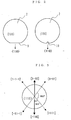
- Fig. 2 illustrates crystal plane orientations, and orientations of an orientation flat and a notch in the second silicon single crystal wafers used in the present invention.
- Fig. 3 shows a crystal plane orientation of the first silicon single crystal wafer and orientations possible to obtain high mobility.
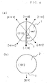
- Figs. 4 show each plane orientation and each orientation of orientation flats of the first and second silicon single crystal wafers used in Example.
- the inventors of the present invention conceived that the aforementioned insulator film is formed on a silicon single crystal wafer having a ⁇ 110 ⁇ plane to produce the MISFET.
- silicon single crystal wafers having a ⁇ 110 ⁇ plane which have been hardly produced in a regular mass production line, were produced, and in order to determine MIS device fabrication process conditions, both a silicon single crystal wafer having a ⁇ 100 ⁇ plane commonly used and a silicon single crystal wafer having a ⁇ 110 ⁇ plane were simultaneously subjected to a heat treatment process, and compared with each other.
- the silicon single crystal wafer having a ⁇ 110 ⁇ plane is very easy to be warped as compared with the silicon single crystal wafer having a ⁇ 100 ⁇ plane.
- Silicon single crystal wafers having a ⁇ 110 ⁇ plane and a ⁇ 100 ⁇ plane, a diameter of 200 mm, and the same standards other than plane orientations were prepared. Each warpage of the silicon single crystal wafers before a heat treatment was 10 ⁇ m or less.
- the warpage in the wafer having the ⁇ 100 ⁇ plane was maintained at 10 ⁇ m or less even after the heat treatment.
- the warpage could not be measured (may be several hundred micrometers or more).
- silicon wafers having ⁇ 110 ⁇ plane had been produced for fabricating various kinds of devices when silicon wafers mainly had a small diameter of 4 inches or less.
- the silicon wafers were not so warped by a heat treatment that continuation of a device fabrication process was interfered.
- the inventors of the present invention conceived that wafers having different plane orientations are bonded to produce a bonded wafer so as to combine an advantage of a MIS device in a silicon single crystal wafer having a ⁇ 110 ⁇ plane with an advantage of mechanical strength in a silicon single crystal wafer having a ⁇ 100 ⁇ plane, and consequently, they accomplished the present invention.
- a bonded SOI wafer produced by an ion implantation delamination method also called a smart cut method (registered trademark) for example.
- an ion implantation delamination method also called a smart cut method (registered trademark) for example.
- the present invention is not limited thereto.
- Fig. 1 is a flowchart showing one example of a production process of a bonded SOI wafer of the present invention.
- a mirror-polished silicon wafer having a crystal plane orientation of ⁇ 110 ⁇ used as a first silicon single crystal wafer 1 to be a silicon single crystal layer on which a device is fabricated is prepared.
- the first silicon single crystal wafer 1 has the plane orientation of ⁇ 110 ⁇ accurately.
- a margin of about 15° is acceptable, the margin is preferably within 10°, and more preferably within 5°.
- a second silicon single crystal wafer 2 is used as a support substrate for supporting the silicon single crystal layer on which a device is fabricated, and if a wafer has a crystal plane orientation of ⁇ 100 ⁇ , the wafer is preferable since the wafer has the plane orientation of high usability for various purposes and good resistance to warpage. Also in this case, when the margin of 15°, preferably within 10°, or more preferably within 5° to the ⁇ 100 ⁇ plane is satisfied, since resistance to warpage becomes high, warpage due to a heat treatment can be lowered as compared with the wafer having the ⁇ 110 ⁇ plane.
- a silicon oxide film 3 to be an insulator film (buried oxide layer) of an SOI wafer having a thickness about several dozen nanometers to two micrometers is formed on a surface of at least one wafer (in this case, the first silicon single crystal wafer 1).
- step (c) hydrogen ions out of hydrogen ions and rare gas ions are implanted in this case from one side of the first silicon single crystal wafer on which the oxide film is formed to form an ion implanted layer (micro bubble layer) 4 parallel to the surface in mean penetration depth of the ions.
- the first silicon single crystal wafer 1 has a plane orientation of ⁇ 110 ⁇ , interstices between silicon atoms are large, and the hydrogen ions to be implanted easily suffer from channeling.
- a concentration distribution of the hydrogen ion implanted layer is being broad along the depth direction, and delamination does not smoothly occur in a subsequent delamination process.
- an angle of implanting hydrogen ions may be possible to be perpendicular to a ⁇ 110 ⁇ plane.
- hydrogen ions are implanted from the surface on which an oxide film is not formed, it is preferable that hydrogen ions are implanted so that the implantation angle is inclined from a direction perpendicular to a ⁇ 110 ⁇ plane.
- the angle to be inclined is preferably about 3-20°. Even when the oxide film is formed on the surface from which hydrogen ions are implanted, by implanting hydrogen ions at an angle inclined from a direction perpendicular to a ⁇ 110 ⁇ plane, the channeling can also be further suppressed.
- the step (d) is a step of superposing and bonding the second silicon single crystal wafer 2 onto the hydrogen ion implanted surface of the first silicon single crystal wafer 1 via the silicon oxide film.
- a wafer having a crystal plane orientation of ⁇ 100 ⁇ and an orientation of an orientation flat (or notch) of ⁇ 110> is used as the second silicon single crystal wafer (see Fig. 2), when the first silicon single crystal wafer is bonded to the second silicon single crystal wafer so that the direction in which the mobility of the first silicon single crystal wafer is increased ([-110] direction or [1-10] direction parallel to the [-110] direction when the first silicon single crystal wafer has a plane orientation of (110): see Fig.
- a source drain direction of a MIS type transistor formed on a silicon single crystal layer 7 corresponds to the ⁇ 110> direction, and thereby, the channel mobility can be easily improved.
- SOI layer silicon single crystal layer 7
- the step (e) is a delaminating heat treatment step in which the bonded wafer is delaminated at an ion-implanted layer 4 as a border to separate into a delaminated wafer 5 and an SOI wafer 6 (the silicon single crystal layer 7 (SOI layer) + buried oxide film 3 + second silicon single crystal wafer 2).
- the bonded wafer is separated into the delaminated wafer 5 and the SOI wafer 6 due to rearrangement of crystals and agglomeration of bubbles.
- a damage layer 8 remains on the SOI layer 7 formed on the surface of the SOI wafer 6 being delaminated.
- a hydrogen ion implantation dose is extremely increased or a bonding strength is increased by surface treatment of the surface to be bonded in the bonding step at a room temperature (a plasma treatment), so that mechanical delamination becomes possible, and therefore, the delaminating heat treatment in the step (e) may not necessarily be needed.
- a bonding heat treatment process is performed in the step (f).
- the SOI wafer 6 is subjected to a heat treatment at a high temperature as a bonding heat treatment to obtain sufficient bonding strength, since the bonding strength of the bonded wafer brought into close contact with each other in the steps (d) and (e) of the aforementioned bonding step and the delaminating heat treatment step would be weak for use in the device production process.
- This heat treatment is preferably performed, for example, under an inert gas atmosphere at 1000-1300°C for 30 minutes to 2 hours. Also, by performing the delaminating heat treatment in the step (e) at a high temperature, the bonding heat treatment step (f) can be omitted.
- step (g) surface roughness of the SOI surface is improved and damages thereon are eliminated.
- a polishing process called a touch polish
- a high temperature annealing under an argon gas or hydrogen gas atmosphere can be performed.
- damages can also be eliminated by a so-called sacrificial oxidation treatment that after thermal oxidation is performed, the resultant oxide film is eliminated, or these steps may be combined properly.
- the bonded wafer of the present invention can be obtained.
- a silicon single crystal ingot produced by a Czochralski method and having a crystal orientation of ⁇ 110>, a conductivity type of P-type, and a resistivity of about 10 ⁇ cm was sliced to produce a silicon single crystal wafer having a diameter of 200 mm and a crystal plane orientation of (110) (the margin of the plane orientation was 1° or less), which was used as a first silicon single crystal wafer (to be an SOI layer).
- an orientation flat was formed in a direction of [-110] on the (110) plane of the first silicon single crystal wafer (see Fig. 4(a)).
- a silicon single crystal ingot produced by a Czochralski method and having a crystal orientation of ⁇ 100>, a conductivity type of P-type, and a resistivity of about 10 ⁇ cm was sliced to produce a silicon single crystal wafer having a diameter of 200 mm and a crystal plane orientation of (100) (the margin of the plane orientation was 1° or less), which was used as a second silicon single crystal wafer (a support substrate).
- an orientation flat was formed in a direction of [011] thereof (see Fig. 4(b)).
- a buried oxide film 3 had a thickness of 400 nm, and the other main conditions such as ion implantation were as follows.
- the SOI wafer 6 having an SOI layer 7 with a thickness of about 300 nm could be obtained.
- the SOI wafer 6 was subjected to a bonding heat treatment under an oxidizing atmosphere at 1100°C for 2 hours. After an oxide film formed on the SOI surface was eliminated with a hydrofluoric acid, the SOI surface was polished about 100 nm so as to completely eliminate damages therefrom and improve surface roughness, and thereby, a bonded SOI wafer having the SOI layer with a thickness of about 100 nm was completed.
- the SOI layer on the bonded SOI wafer completed had the crystal plane orientation of (110), but the support substrate had the crystal plane orientation of (100), mechanical strength of the bonded SOI wafer (resistance to warpage due to heat treatment) was obtained at the equal level as a usual (100) wafer. And, since the wafers were bonded so that each orientation flat of the wafers corresponded to each other when bonding the wafers, the direction easy to cleave a support substrate corresponded to the direction in which high carrier mobility was obtained when fabricating a MIS device on the SOI layer, and thereby, the bonded SOI wafer was easily processed into rectangular chips, and its processing loss could be lowered.
- the present invention is not limited thereto and can employ a method that, for example, after two wafers are bonded, one wafer is ground and polished to be made into a thin film or a method that a porous layer is formed on a surface of one wafer, an epitaxial layer is formed on the porous layer, a surface of the epitaxial layer is bonded to a surface of the other wafer, and the resultant wafer is delaminated at the porous layer.
- the wafer having a (110) plane is used as the first silicon single crystal wafer, and the orientation flat is formed in the [-110] direction thereof.
- the same effects as in the Example can be obtained when a wafer having an equivalent plane orientation to the (110) wafer, which is not the (110) wafer as it is, and having an orientation flat formed in a direction of the wafer having an equivalent relation to a [-110] direction for the (110) plane is used.
- the case that the bonded wafer having a diameter of 200 mm is produced is explained by way of examples.
- the present invention is not limited thereto, and in particular, since wafers will be more warped easily than before when diameters of the wafers are reached to 300 mm or more in the future, it is more effective to apply the present invention to the bonded wafers.
Landscapes
- Recrystallisation Techniques (AREA)
- Thin Film Transistor (AREA)
- Metal-Oxide And Bipolar Metal-Oxide Semiconductor Integrated Circuits (AREA)
- Element Separation (AREA)
Abstract
Description
Claims (13)
- A bonded wafer, wherein at least a silicon single crystal layer is formed on a silicon single crystal wafer, the silicon single crystal layer has a crystal plane orientation of {110}, and the silicon single crystal wafer has a crystal plane orientation of {100}.
- The bonded wafer according to Claim 1,
wherein the silicon single crystal layer has a crystal plane orientation tilting within 15° from the crystal plane orientation of {110}, and the silicon single crystal wafer has a crystal plane orientation tilting within 15° from the crystal plane orientation of {100}. - The bonded wafer according to Claim 1 or Claim 2, wherein an insulator film is provided between the silicon single crystal wafer and the silicon single crystal layer.
- The bonded wafer according to any one of Claims 1-3, wherein the silicon single crystal layer has a crystal plane orientation of (110), and a [-110] direction of the (110) plane is parallel or perpendicular to a <110> direction of the silicon single crystal wafer.
- The bonded wafer according to any one of Claims 1-4, which has a diameter of 200 mm or more.
- A method of producing a bonded wafer,
wherein after at least a first silicon single crystal wafer having a crystal plane orientation of {110} and a second silicon single crystal wafer having a crystal plane orientation of {100} are bonded directly or bonded via an insulator film, the first silicon single crystal wafer is made into a thin film. - A method of producing a bonded wafer,
wherein after at least hydrogen ions or rare gas ions are implanted from a surface of a first silicon single crystal wafer to form an ion implanted layer in the first silicon single crystal wafer, and after the first silicon single crystal wafer is bonded to a second silicon single crystal wafer, the first silicon single crystal wafer is delaminated at the ion implanted layer, and wherein a silicon single crystal wafer having a crystal plane orientation of {110} is used as the first silicon single crystal wafer, and a silicon single crystal wafer having a crystal plane orientation of {100} is used as the second silicon single crystal wafer. - The method of producing a bonded wafer according to Claim 7, wherein an implantation angle of the ions implanted from the surface of the first silicon single crystal wafer is inclined from a direction perpendicular to the {110} plane.
- The method of producing a bonded wafer according to Claim 7 or Claim 8, wherein after an insulator film is formed on the surface of the first silicon single crystal wafer, the ions are implanted into the first silicon single crystal wafer through the insulator film.
- The method of producing a bonded wafer according to any one of Claims 7-9, wherein after an insulator film is formed on the surface of the second single crystal wafer, the second silicon single crystal wafer is bonded to the first silicon single crystal wafer via the insulator film.
- The method of producing a bonded wafer according to any one of Claims 6-10, wherein a wafer having a crystal plane orientation tilting within 15° from the crystal plane orientation of {110} is used as the first silicon single crystal wafer, and a wafer having a crystal plane orientation tilting within 15° from the crystal plane orientation of {100} is used as the second silicon single crystal wafer.
- The method of producing a bonded wafer according to any one of Claims 6-11, wherein a wafer having a crystal plane orientation of (110) is used as the first silicon single crystal wafer, and the first silicon single crystal wafer and the second silicon single crystal wafer are bonded so that a [-110] direction of the (110) plane is parallel or perpendicular to a <110> direction of the second silicon single crystal wafer.
- The method of producing a bonded wafer according to any one of Claims 6-12, wherein each wafer used for the first silicon single crystal wafer and the second silicon single crystal wafer has a diameter of 200 mm or more.
Applications Claiming Priority (3)
| Application Number | Priority Date | Filing Date | Title |
|---|---|---|---|
| JP2001370680 | 2001-12-04 | ||
| JP2001370680 | 2001-12-04 | ||
| PCT/JP2002/012277 WO2003049189A1 (en) | 2001-12-04 | 2002-11-25 | Pasted wafer and method for producing pasted wafer |
Publications (3)
| Publication Number | Publication Date |
|---|---|
| EP1453096A1 true EP1453096A1 (en) | 2004-09-01 |
| EP1453096A4 EP1453096A4 (en) | 2009-10-28 |
| EP1453096B1 EP1453096B1 (en) | 2017-02-22 |
Family
ID=19179863
Family Applications (1)
| Application Number | Title | Priority Date | Filing Date |
|---|---|---|---|
| EP02783616.2A Expired - Lifetime EP1453096B1 (en) | 2001-12-04 | 2002-11-25 | Method for producing a bonded wafer |
Country Status (7)
| Country | Link |
|---|---|
| US (2) | US7052974B2 (en) |
| EP (1) | EP1453096B1 (en) |
| JP (1) | JPWO2003049189A1 (en) |
| KR (1) | KR20050044643A (en) |
| CN (1) | CN100403543C (en) |
| TW (1) | TWI290735B (en) |
| WO (1) | WO2003049189A1 (en) |
Cited By (3)
| Publication number | Priority date | Publication date | Assignee | Title |
|---|---|---|---|---|
| WO2006053890A1 (en) * | 2004-11-18 | 2006-05-26 | International Business Machines Corporation | Soi substrate materials and method to form si-containing soi and underlying substrate with different orientations |
| WO2006103491A1 (en) * | 2005-03-29 | 2006-10-05 | S.O.I.Tec Silicon On Insulator Technologies | Hybrid fully soi-type multilayer structure |
| EP2040285A1 (en) * | 2007-09-19 | 2009-03-25 | S.O.I. TEC Silicon | Method for fabricating a mixed orientation substrate |
Families Citing this family (62)
| Publication number | Priority date | Publication date | Assignee | Title |
|---|---|---|---|---|
| JP3635200B2 (en) * | 1998-06-04 | 2005-04-06 | 信越半導体株式会社 | Manufacturing method of SOI wafer |
| JP4947248B2 (en) * | 2001-09-14 | 2012-06-06 | Dowaエレクトロニクス株式会社 | Notched compound semiconductor wafer |
| CN100403543C (en) * | 2001-12-04 | 2008-07-16 | 信越半导体株式会社 | Bonded wafer and method for manufacturing bonded wafer |
| US6784071B2 (en) * | 2003-01-31 | 2004-08-31 | Taiwan Semiconductor Manufacturing Company, Ltd. | Bonded SOI wafer with <100> device layer and <110> substrate for performance improvement |
| JP4190906B2 (en) * | 2003-02-07 | 2008-12-03 | 信越半導体株式会社 | Silicon semiconductor substrate and manufacturing method thereof |
| JP4816856B2 (en) * | 2004-09-15 | 2011-11-16 | 信越半導体株式会社 | Manufacturing method of SOI wafer |
| JP3979412B2 (en) * | 2004-09-29 | 2007-09-19 | 株式会社Sumco | Manufacturing method of silicon epitaxial wafer |
| EP1681712A1 (en) * | 2005-01-13 | 2006-07-19 | S.O.I. Tec Silicon on Insulator Technologies S.A. | Method of producing substrates for optoelectronic applications |
| JP4624812B2 (en) * | 2005-01-20 | 2011-02-02 | 信越化学工業株式会社 | Manufacturing method of SOI wafer |
| US7494899B2 (en) * | 2005-04-14 | 2009-02-24 | Sumco Corporation | Method for manufacturing semiconductor substrate |
| US7635637B2 (en) * | 2005-07-25 | 2009-12-22 | Fairchild Semiconductor Corporation | Semiconductor structures formed on substrates and methods of manufacturing the same |
| JP2007173354A (en) | 2005-12-20 | 2007-07-05 | Shin Etsu Chem Co Ltd | SOI substrate and method for manufacturing SOI substrate |
| JP5109287B2 (en) * | 2006-05-09 | 2012-12-26 | 株式会社Sumco | Manufacturing method of semiconductor substrate |
| JP5082299B2 (en) * | 2006-05-25 | 2012-11-28 | 株式会社Sumco | Manufacturing method of semiconductor substrate |
| JP2008153411A (en) * | 2006-12-18 | 2008-07-03 | Shin Etsu Chem Co Ltd | Manufacturing method of SOI substrate |
| FR2912258B1 (en) * | 2007-02-01 | 2009-05-08 | Soitec Silicon On Insulator | "METHOD OF MANUFACTURING A SUBSTRATE OF THE SILICON TYPE ON INSULATION" |
| KR100857165B1 (en) * | 2007-04-13 | 2008-09-05 | 삼성전기주식회사 | Circuit Board Manufacturing Method |
| EP1993130A3 (en) * | 2007-05-17 | 2011-09-07 | Semiconductor Energy Laboratory Co., Ltd. | Semiconductor device and method for manufacturing the same |
| EP1993128A3 (en) * | 2007-05-17 | 2010-03-24 | Semiconductor Energy Laboratory Co., Ltd. | Method for manufacturing soi substrate |
| WO2008149699A1 (en) * | 2007-06-01 | 2008-12-11 | Semiconductor Energy Laboratory Co., Ltd. | Manufacturing method of semiconductor substrate and semiconductor device |
| EP2174343A1 (en) * | 2007-06-28 | 2010-04-14 | Semiconductor Energy Laboratory Co, Ltd. | Manufacturing method of semiconductor device |
| JP5498670B2 (en) * | 2007-07-13 | 2014-05-21 | 株式会社半導体エネルギー研究所 | Method for manufacturing semiconductor substrate |
| JP4888276B2 (en) * | 2007-08-09 | 2012-02-29 | 三菱電機株式会社 | Semiconductor wafer equipment |
| JP5460984B2 (en) * | 2007-08-17 | 2014-04-02 | 株式会社半導体エネルギー研究所 | Method for manufacturing semiconductor device |
| JP5268305B2 (en) * | 2007-08-24 | 2013-08-21 | 株式会社半導体エネルギー研究所 | Method for manufacturing semiconductor device |
| JP2009076879A (en) | 2007-08-24 | 2009-04-09 | Semiconductor Energy Lab Co Ltd | Semiconductor device |
| CN101796613B (en) * | 2007-09-14 | 2012-06-27 | 株式会社半导体能源研究所 | Semiconductor devices and electronic equipment |
| US8232598B2 (en) * | 2007-09-20 | 2012-07-31 | Semiconductor Energy Laboratory Co., Ltd. | Display device and method for manufacturing the same |
| US8044464B2 (en) * | 2007-09-21 | 2011-10-25 | Semiconductor Energy Laboratory Co., Ltd. | Semiconductor device |
| US8101500B2 (en) | 2007-09-27 | 2012-01-24 | Fairchild Semiconductor Corporation | Semiconductor device with (110)-oriented silicon |
| JP5522917B2 (en) | 2007-10-10 | 2014-06-18 | 株式会社半導体エネルギー研究所 | Manufacturing method of SOI substrate |
| TWI493609B (en) * | 2007-10-23 | 2015-07-21 | 半導體能源研究所股份有限公司 | Semiconductor substrate, display panel, and method of manufacturing display device |
| JP5394043B2 (en) * | 2007-11-19 | 2014-01-22 | 株式会社半導体エネルギー研究所 | Semiconductor substrate, semiconductor device using the same, and manufacturing method thereof |
| JP5190669B2 (en) * | 2008-01-16 | 2013-04-24 | 信越半導体株式会社 | Manufacturing method of bonded wafer |
| US7820527B2 (en) * | 2008-02-20 | 2010-10-26 | Varian Semiconductor Equipment Associates, Inc. | Cleave initiation using varying ion implant dose |
| JP2009231376A (en) * | 2008-03-19 | 2009-10-08 | Shin Etsu Handotai Co Ltd | Soi wafer and semiconductor device, and method of manufacturing the soi wafer |
| US8039877B2 (en) * | 2008-09-09 | 2011-10-18 | Fairchild Semiconductor Corporation | (110)-oriented p-channel trench MOSFET having high-K gate dielectric |
| JP2010067930A (en) * | 2008-09-12 | 2010-03-25 | Toshiba Corp | Semiconductor device and method of manufacturing the same |
| US7928534B2 (en) * | 2008-10-09 | 2011-04-19 | Taiwan Semiconductor Manufacturing Company, Ltd. | Bond pad connection to redistribution lines having tapered profiles |
| US8736050B2 (en) * | 2009-09-03 | 2014-05-27 | Taiwan Semiconductor Manufacturing Company, Ltd. | Front side copper post joint structure for temporary bond in TSV application |
| US8759949B2 (en) * | 2009-04-30 | 2014-06-24 | Taiwan Semiconductor Manufacturing Company, Ltd. | Wafer backside structures having copper pillars |
| US8278187B2 (en) * | 2009-06-24 | 2012-10-02 | Semiconductor Energy Laboratory Co., Ltd. | Method for reprocessing semiconductor substrate by stepwise etching with at least two etching treatments |
| SG176602A1 (en) * | 2009-06-24 | 2012-01-30 | Semiconductor Energy Lab | Method for reprocessing semiconductor substrate and method for manufacturing soi substrate |
| US8158489B2 (en) * | 2009-06-26 | 2012-04-17 | Taiwan Semiconductor Manufacturing Company, Ltd. | Formation of TSV backside interconnects by modifying carrier wafers |
| SG178061A1 (en) * | 2009-08-25 | 2012-03-29 | Semiconductor Energy Lab | Method for reprocessing semiconductor substrate, method for manufacturing reprocessed semiconductor substrate, and method for manufacturing soi substrate |
| US8318588B2 (en) * | 2009-08-25 | 2012-11-27 | Semiconductor Energy Laboratory Co., Ltd. | Method for reprocessing semiconductor substrate, method for manufacturing reprocessed semiconductor substrate, and method for manufacturing SOI substrate |
| WO2011043178A1 (en) * | 2009-10-09 | 2011-04-14 | Semiconductor Energy Laboratory Co., Ltd. | Reprocessing method of semiconductor substrate, manufacturing method of reprocessed semiconductor substrate, and manufacturing method of soi substrate |
| JP5643509B2 (en) * | 2009-12-28 | 2014-12-17 | 信越化学工業株式会社 | SOS substrate manufacturing method with reduced stress |
| JP2011198962A (en) * | 2010-03-18 | 2011-10-06 | Toshiba Corp | Method for manufacturing semiconductor light emitting element |
| US8174124B2 (en) | 2010-04-08 | 2012-05-08 | Taiwan Semiconductor Manufacturing Co., Ltd. | Dummy pattern in wafer backside routing |
| JP5601071B2 (en) * | 2010-07-30 | 2014-10-08 | トヨタ自動車株式会社 | How to peel off the protective tape |
| KR20120020526A (en) * | 2010-08-30 | 2012-03-08 | 삼성전자주식회사 | Substrate have buried conductive layer and formation method thereof, and fabricating method of semiconductor device using the same |
| US9123529B2 (en) | 2011-06-21 | 2015-09-01 | Semiconductor Energy Laboratory Co., Ltd. | Method for reprocessing semiconductor substrate, method for manufacturing reprocessed semiconductor substrate, and method for manufacturing SOI substrate |
| CN107146758B (en) | 2016-12-27 | 2019-12-13 | 上海新傲科技股份有限公司 | Preparation method of substrate with carrier trapping center |
| CN106601615B (en) * | 2016-12-27 | 2020-05-15 | 上海新傲科技股份有限公司 | Annealing method for improving bonding strength |
| CN106783725B (en) | 2016-12-27 | 2019-09-17 | 上海新傲科技股份有限公司 | The preparation method of substrate with insulating buried layer |
| CN106683980B (en) * | 2016-12-27 | 2019-12-13 | 上海新傲科技股份有限公司 | Preparation method of substrate with carrier trapping center |
| JP6686962B2 (en) * | 2017-04-25 | 2020-04-22 | 信越半導体株式会社 | Method for manufacturing bonded wafer |
| JP6834816B2 (en) | 2017-07-10 | 2021-02-24 | 株式会社Sumco | Silicon wafer processing method |
| CN109830617A (en) * | 2019-01-14 | 2019-05-31 | 深圳市华星光电半导体显示技术有限公司 | Abutted equipment |
| FR3108440B1 (en) * | 2020-03-23 | 2025-01-17 | Soitec Silicon On Insulator | Method of preparing a thin layer |
| KR102877317B1 (en) * | 2020-10-30 | 2025-10-27 | 삼성전자주식회사 | Semiconductor wafer and method for fabricating the same |
Family Cites Families (14)
| Publication number | Priority date | Publication date | Assignee | Title |
|---|---|---|---|---|
| NL171309C (en) * | 1970-03-02 | 1983-03-01 | Hitachi Ltd | METHOD FOR THE MANUFACTURE OF A SEMICONDUCTOR BODY FORMING A SILICONE DIOXIDE LAYER ON A SURFACE OF A SILICONE MONOCRYSTALLINE BODY |
| TW211621B (en) * | 1991-07-31 | 1993-08-21 | Canon Kk | |
| JPH0590117A (en) * | 1991-09-27 | 1993-04-09 | Toshiba Corp | Single crystal thin film semiconductor device |
| JP3237888B2 (en) * | 1992-01-31 | 2001-12-10 | キヤノン株式会社 | Semiconductor substrate and method of manufacturing the same |
| JPH05340828A (en) * | 1992-05-18 | 1993-12-24 | Fujikura Ltd | Semiconductor pressure sensor |
| JPH07335511A (en) * | 1994-06-13 | 1995-12-22 | Nippon Telegr & Teleph Corp <Ntt> | Bonded wafer |
| SG67458A1 (en) * | 1996-12-18 | 1999-09-21 | Canon Kk | Process for producing semiconductor article |
| JP3395661B2 (en) * | 1998-07-07 | 2003-04-14 | 信越半導体株式会社 | Method for manufacturing SOI wafer |
| JP3358550B2 (en) * | 1998-07-07 | 2002-12-24 | 信越半導体株式会社 | Method for producing SOI wafer and SOI wafer produced by this method |
| JP2000124092A (en) * | 1998-10-16 | 2000-04-28 | Shin Etsu Handotai Co Ltd | Method of manufacturing SOI wafer by hydrogen ion implantation separation method and SOI wafer manufactured by this method |
| JP3900741B2 (en) * | 1999-05-21 | 2007-04-04 | 信越半導体株式会社 | Manufacturing method of SOI wafer |
| EP1158581B1 (en) * | 1999-10-14 | 2016-04-27 | Shin-Etsu Handotai Co., Ltd. | Method for producing soi wafer |
| US6566233B2 (en) * | 1999-12-24 | 2003-05-20 | Shin-Etsu Handotai Co., Ltd. | Method for manufacturing bonded wafer |
| CN100403543C (en) * | 2001-12-04 | 2008-07-16 | 信越半导体株式会社 | Bonded wafer and method for manufacturing bonded wafer |
-
2002
- 2002-11-25 CN CNB028242955A patent/CN100403543C/en not_active Expired - Lifetime
- 2002-11-25 WO PCT/JP2002/012277 patent/WO2003049189A1/en not_active Ceased
- 2002-11-25 KR KR1020047008428A patent/KR20050044643A/en not_active Ceased
- 2002-11-25 US US10/496,379 patent/US7052974B2/en not_active Expired - Lifetime
- 2002-11-25 JP JP2003550285A patent/JPWO2003049189A1/en active Pending
- 2002-11-25 EP EP02783616.2A patent/EP1453096B1/en not_active Expired - Lifetime
- 2002-11-29 TW TW091134820A patent/TWI290735B/en not_active IP Right Cessation
-
2005
- 2005-12-15 US US11/300,503 patent/US7315064B2/en not_active Expired - Lifetime
Cited By (5)
| Publication number | Priority date | Publication date | Assignee | Title |
|---|---|---|---|---|
| WO2006053890A1 (en) * | 2004-11-18 | 2006-05-26 | International Business Machines Corporation | Soi substrate materials and method to form si-containing soi and underlying substrate with different orientations |
| CN100533706C (en) * | 2004-11-18 | 2009-08-26 | 国际商业机器公司 | SOI substrate materials and method to form Si-containing SOI and underlying substrate with different orientations |
| WO2006103491A1 (en) * | 2005-03-29 | 2006-10-05 | S.O.I.Tec Silicon On Insulator Technologies | Hybrid fully soi-type multilayer structure |
| EP2040285A1 (en) * | 2007-09-19 | 2009-03-25 | S.O.I. TEC Silicon | Method for fabricating a mixed orientation substrate |
| WO2009036950A3 (en) * | 2007-09-19 | 2009-06-25 | Soitec Silicon On Insulator | Method for fabricating a mixed orientation substrate |
Also Published As
| Publication number | Publication date |
|---|---|
| KR20050044643A (en) | 2005-05-12 |
| EP1453096A4 (en) | 2009-10-28 |
| CN100403543C (en) | 2008-07-16 |
| CN1599958A (en) | 2005-03-23 |
| US20050003648A1 (en) | 2005-01-06 |
| US20060099791A1 (en) | 2006-05-11 |
| US7052974B2 (en) | 2006-05-30 |
| TWI290735B (en) | 2007-12-01 |
| US7315064B2 (en) | 2008-01-01 |
| JPWO2003049189A1 (en) | 2005-04-21 |
| EP1453096B1 (en) | 2017-02-22 |
| WO2003049189A1 (en) | 2003-06-12 |
| TW200300969A (en) | 2003-06-16 |
Similar Documents
| Publication | Publication Date | Title |
|---|---|---|
| US7315064B2 (en) | Bonded wafer and method of producing bonded wafer | |
| US7825470B2 (en) | Transistor and in-situ fabrication process | |
| US6054363A (en) | Method of manufacturing semiconductor article | |
| US20090032873A1 (en) | Ultra thin single crystalline semiconductor TFT and process for making same | |
| CN1954421A (en) | Method of forming strained Si/SiGe on insulator with silicon germanium buffer | |
| CN103038863A (en) | Oxygen plasma conversion process for preparing a surface for bonding | |
| JP2002164520A (en) | Manufacturing method of semiconductor wafer | |
| KR101142138B1 (en) | Multilayer Substrate Cleaning Method, Substrate Bonding Method, And Bonded Wafer Manufacturing Method | |
| CN101681805A (en) | Soi wafer manufacturing method | |
| EP2256787A1 (en) | Process for producing soi wafer | |
| JP2002184960A (en) | SOI wafer manufacturing method and SOI wafer | |
| US20080164572A1 (en) | Semiconductor substrate and manufacturing method thereof | |
| US20090004825A1 (en) | Method of manufacturing semiconductor substrate | |
| WO1999039380A1 (en) | Soi substrate and method for manufacturing the same | |
| JP4239676B2 (en) | SOI wafer and manufacturing method thereof | |
| JPH11330438A (en) | Manufacture of soi wafer and soi wafer | |
| KR100765860B1 (en) | Simox substrate and method for production thereof | |
| KR100704146B1 (en) | Manufacturing method of SOI substrate | |
| CN122073992A (en) | Silicon-on-insulator substrates and their fabrication methods | |
| JP2000068489A (en) | SOI substrate and method of manufacturing the same | |
| JP2002289819A (en) | SIMOX substrate | |
| JP2008159868A (en) | Method for manufacturing simox substrate |
Legal Events
| Date | Code | Title | Description |
|---|---|---|---|
| PUAI | Public reference made under article 153(3) epc to a published international application that has entered the european phase |
Free format text: ORIGINAL CODE: 0009012 |
|
| 17P | Request for examination filed |
Effective date: 20040602 |
|
| AK | Designated contracting states |
Kind code of ref document: A1 Designated state(s): AT BE BG CH CY CZ DE DK EE ES FI FR GB GR IE IT LI LU MC NL PT SE SK TR |
|
| RAP1 | Party data changed (applicant data changed or rights of an application transferred) |
Owner name: SHIN-ETSU HANDOTAI CO., LTD. |
|
| A4 | Supplementary search report drawn up and despatched |
Effective date: 20090928 |
|
| RIC1 | Information provided on ipc code assigned before grant |
Ipc: H01L 27/12 20060101ALI20090922BHEP Ipc: H01L 21/762 20060101ALI20090922BHEP Ipc: H01L 29/04 20060101AFI20090922BHEP |
|
| 17Q | First examination report despatched |
Effective date: 20120410 |
|
| RAP1 | Party data changed (applicant data changed or rights of an application transferred) |
Owner name: SHIN-ETSU HANDOTAI CO., LTD. |
|
| GRAP | Despatch of communication of intention to grant a patent |
Free format text: ORIGINAL CODE: EPIDOSNIGR1 |
|
| INTG | Intention to grant announced |
Effective date: 20160908 |
|
| GRAS | Grant fee paid |
Free format text: ORIGINAL CODE: EPIDOSNIGR3 |
|
| STAA | Information on the status of an ep patent application or granted ep patent |
Free format text: STATUS: GRANT OF PATENT IS INTENDED |
|
| GRAJ | Information related to disapproval of communication of intention to grant by the applicant or resumption of examination proceedings by the epo deleted |
Free format text: ORIGINAL CODE: EPIDOSDIGR1 |
|
| GRAL | Information related to payment of fee for publishing/printing deleted |
Free format text: ORIGINAL CODE: EPIDOSDIGR3 |
|
| STAA | Information on the status of an ep patent application or granted ep patent |
Free format text: STATUS: EXAMINATION IS IN PROGRESS |
|
| GRAR | Information related to intention to grant a patent recorded |
Free format text: ORIGINAL CODE: EPIDOSNIGR71 |
|
| STAA | Information on the status of an ep patent application or granted ep patent |
Free format text: STATUS: GRANT OF PATENT IS INTENDED |
|
| GRAA | (expected) grant |
Free format text: ORIGINAL CODE: 0009210 |
|
| STAA | Information on the status of an ep patent application or granted ep patent |
Free format text: STATUS: THE PATENT HAS BEEN GRANTED |
|
| INTC | Intention to grant announced (deleted) | ||
| AK | Designated contracting states |
Kind code of ref document: B1 Designated state(s): DE FR |
|
| INTG | Intention to grant announced |
Effective date: 20170117 |
|
| REG | Reference to a national code |
Ref country code: DE Ref legal event code: R096 Ref document number: 60248683 Country of ref document: DE |
|
| REG | Reference to a national code |
Ref country code: FR Ref legal event code: PLFP Year of fee payment: 16 |
|
| REG | Reference to a national code |
Ref country code: DE Ref legal event code: R097 Ref document number: 60248683 Country of ref document: DE |
|
| PLBE | No opposition filed within time limit |
Free format text: ORIGINAL CODE: 0009261 |
|
| STAA | Information on the status of an ep patent application or granted ep patent |
Free format text: STATUS: NO OPPOSITION FILED WITHIN TIME LIMIT |
|
| 26N | No opposition filed |
Effective date: 20171123 |
|
| REG | Reference to a national code |
Ref country code: FR Ref legal event code: PLFP Year of fee payment: 17 |
|
| PGFP | Annual fee paid to national office [announced via postgrant information from national office to epo] |
Ref country code: FR Payment date: 20211109 Year of fee payment: 20 Ref country code: DE Payment date: 20210929 Year of fee payment: 20 |
|
| REG | Reference to a national code |
Ref country code: DE Ref legal event code: R071 Ref document number: 60248683 Country of ref document: DE |