JP2011198962A - Method for manufacturing semiconductor light emitting element - Google Patents
Method for manufacturing semiconductor light emitting element Download PDFInfo
- Publication number
- JP2011198962A JP2011198962A JP2010063288A JP2010063288A JP2011198962A JP 2011198962 A JP2011198962 A JP 2011198962A JP 2010063288 A JP2010063288 A JP 2010063288A JP 2010063288 A JP2010063288 A JP 2010063288A JP 2011198962 A JP2011198962 A JP 2011198962A
- Authority
- JP
- Japan
- Prior art keywords
- substrate
- stacked body
- metal layer
- laminate
- light emitting
- Prior art date
- Legal status (The legal status is an assumption and is not a legal conclusion. Google has not performed a legal analysis and makes no representation as to the accuracy of the status listed.)
- Pending
Links
Images


Classifications
-
- H—ELECTRICITY
- H01—ELECTRIC ELEMENTS
- H01L—SEMICONDUCTOR DEVICES NOT COVERED BY CLASS H10
- H01L33/00—Semiconductor devices with at least one potential-jump barrier or surface barrier specially adapted for light emission; Processes or apparatus specially adapted for the manufacture or treatment thereof or of parts thereof; Details thereof
- H01L33/005—Processes
- H01L33/0095—Post-treatment of devices, e.g. annealing, recrystallisation or short-circuit elimination
-
- H—ELECTRICITY
- H01—ELECTRIC ELEMENTS
- H01L—SEMICONDUCTOR DEVICES NOT COVERED BY CLASS H10
- H01L33/00—Semiconductor devices with at least one potential-jump barrier or surface barrier specially adapted for light emission; Processes or apparatus specially adapted for the manufacture or treatment thereof or of parts thereof; Details thereof
- H01L33/005—Processes
- H01L33/0093—Wafer bonding; Removal of the growth substrate
Landscapes
- Engineering & Computer Science (AREA)
- Manufacturing & Machinery (AREA)
- Computer Hardware Design (AREA)
- Microelectronics & Electronic Packaging (AREA)
- Power Engineering (AREA)
- Led Devices (AREA)
- Semiconductor Lasers (AREA)
Abstract
Description
本発明は、半導体発光素子の製造方法に関する。 The present invention relates to a method for manufacturing a semiconductor light emitting device.
発光ダイオード(Light Emitting Diode:LED)など半導体発光素子では、発光層を含む半導体層を成長基板から分離し、別の基板に移し替える製造方法が用いられている。例えば、特許文献1には、発光層を含むIII族窒化物半導体層を成長基板から分離し、成長基板とは異なる基板に設けることにより、生産性を向上させることができるIII族窒化物半導体発光素子が記載されている。 In a semiconductor light emitting device such as a light emitting diode (LED), a manufacturing method is used in which a semiconductor layer including a light emitting layer is separated from a growth substrate and transferred to another substrate. For example, Patent Document 1 discloses a group III nitride semiconductor light emitting device that can improve productivity by separating a group III nitride semiconductor layer including a light emitting layer from a growth substrate and providing it on a substrate different from the growth substrate. An element is described.
しかしながら、半導体層を異なる基板上に移し替える際に、2つの基板を重ね合わせて接合するために加えられる加重により、基板の割れやクラックを生じる場合があり、製造歩留りを低下させる要因となっている。そこで、基板の割れやクラックを防ぐことができる製造方法が求められている。 However, when the semiconductor layer is transferred onto a different substrate, the load applied to overlap and bond the two substrates may cause cracking or cracking of the substrate, causing a reduction in manufacturing yield. Yes. Therefore, there is a demand for a manufacturing method that can prevent the substrate from cracking or cracking.
本発明は、2つの基板を接合する際の割れやクラックを抑制し、製造歩留りを向上させる半導体発光素子の製造方法を提供することを目的とする。 An object of this invention is to provide the manufacturing method of the semiconductor light-emitting device which suppresses the crack at the time of joining two board | substrates, and improves a manufacturing yield.
本発明の一態様によれば、第1の基板、半導体層及び第1の金属層を有する第1の積層体と、第2の基板及び第2の金属層を有する第2の積層体と、を貼り合わせる半導体発光素子の製造方法であって、前記第1の積層体の劈開方向と前記第2の積層体の劈開方向とをずらし、前記第1の金属層と前記第2の金属層とを接触させて重ね合わせる工程と、前記第1の基板と前記第2の基板との間に加重を加えた状態で昇温し、前記第1の積層体と前記第2の積層体とを貼り合わせる工程と、を備えたことを特徴とする半導体発光素子の製造方法が提供される。 According to one embodiment of the present invention, a first stack having a first substrate, a semiconductor layer, and a first metal layer, a second stack having a second substrate and a second metal layer, A method of manufacturing a semiconductor light emitting device, wherein the cleavage direction of the first stacked body and the cleavage direction of the second stacked body are shifted, and the first metal layer and the second metal layer are A step of bringing the first laminate and the second laminate together, and a step of bringing the first laminate and the second laminate together to increase the temperature while applying a load between the first substrate and the second substrate. A method for manufacturing a semiconductor light emitting device, comprising:
本発明によれば、2つの基板を接合する際の割れやクラックを抑制し、製造歩留りを向上させる半導体発光素子の製造方法を実現することができる。 ADVANTAGE OF THE INVENTION According to this invention, the manufacturing method of the semiconductor light-emitting device which suppresses the crack at the time of joining two board | substrates, and improves a manufacture yield is realizable.
以下、本発明の実施の形態について図面を参照しながら説明する。なお、以下の実施形態では、図面中の同一部分には同一番号を付してその詳しい説明は適宜省略し、異なる部分について適宜説明する。 Hereinafter, embodiments of the present invention will be described with reference to the drawings. In the following embodiments, the same parts in the drawings are denoted by the same reference numerals, detailed description thereof will be omitted as appropriate, and different parts will be described as appropriate.
本発明の一実施形態に係る半導体発光素子の製造方法は、第1の基板上に第1の金属層が設けられた第1の積層体と、第2の基板上に第2の金属層が設けられた第2の積層体とを、第1の基板の劈開方向と第2の基板の劈開方向とをずらし、第1の金属層と第2の金属層とを接触させて重ね合わせる工程を備えている。第1の積層体は、第1の基板上に発光光を放射する発光層を含む半導体層を有し、第1の金属層は半導体層の上に設けられている。 A method for manufacturing a semiconductor light emitting device according to an embodiment of the present invention includes: a first stacked body in which a first metal layer is provided on a first substrate; and a second metal layer on a second substrate. A step of overlapping the provided second stacked body by shifting the cleavage direction of the first substrate and the cleavage direction of the second substrate and bringing the first metal layer and the second metal layer into contact with each other; I have. The first stacked body includes a semiconductor layer including a light emitting layer that emits light emitted on a first substrate, and the first metal layer is provided on the semiconductor layer.
さらに、第1の積層体と第2の積層体との間に加重を加えた状態で昇温し、第1の積層体と第2の積層体を貼り合わせる工程と、を備えている。 Further, the method includes a step of raising the temperature while applying a load between the first stacked body and the second stacked body, and bonding the first stacked body and the second stacked body.
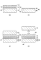
図1は、本発明の一実施形態に係る半導体発光素子の製造方法を模式的に示す工程断面図である。本実施形態に係る製造方法では、例えば、第1の基板をn型GaAs基板10とし、第2の基板をp型シリコン(Si)基板30として説明する。さらに、n型GaAs基板10上に設けられる半導体層12は、例えば、InGaAlP系半導体を含むものである。
FIG. 1 is a process cross-sectional view schematically showing a method for manufacturing a semiconductor light emitting device according to an embodiment of the present invention. In the manufacturing method according to this embodiment, for example, the first substrate is described as an n-
図1(a)は、半導体層12が設けられた第1の積層体20の断面を示し、図1(b)は、第2の積層体40の断面を示している。図1(c)は、第1の積層体20の上に第2の積層体40を重ね合わせた状態を示す断面図である。図1(d)は、半導体層12を第2の積層体40上に残し、n型GaAs基板10を除去した状態を示す断面図である。
FIG. 1A shows a cross section of the first stacked
図1(a)に示すように、n型GaAs基板10の上に、InGaAlPなどを含む半導体層12を、例えば、MOCVD(Metal Organic Chemical Vapor Deposition)法またはMBE(Molecular Beam Epitaxy)法などを用いて形成し、さらに第1の金属層15を形成し、第1の積層体20とする。
一方、図1(b)に示すように、p型Si基板30の上に、第2の金属層35を、真空蒸着法などを用いて形成し、第2の積層体40とする。
As shown in FIG. 1A, a
On the other hand, as shown in FIG. 1B, the
半導体層12に含まれる発光層13がInGaAlP系半導体の場合、半導体発光素子は、黄緑から赤色の波長範囲の可視光を放出することが可能となる。InGaAlP系化合物結晶からなる半導体層12は、GaAsに格子整合するので容易に良好な結晶を設けることができる。
When the
次に、図1(c)に示すように、第2の積層体40の上に第1の積層体20を重ね合わせ、接合界面47において第1の金属層15及び第2の金属層35を接触させる。さらに、所定の基板接合プロセスを施して、第1の積層体20と第2の積層体40とを貼り合わせる。この際、第1の積層体20の劈開方向と、第2の積層体40の劈開方向と、をずらして接合する。
Next, as shown in FIG. 1C, the first stacked
例えば、第1の積層体20の劈開方向は、n型GaAs基板10の劈開方向に一致し、第2の積層体40の劈開方向40は、p型Si基板30の劈開方向に一致する。したがって、n型GaAs基板10の主面25が(100)面であり、p型Si基板30の主面45が(100)面であれば、n型GaAs基板10の〈110〉方向と、p型Si基板30の〈110〉方向とをずらして重ね合わせ、接合させる。
For example, the cleavage direction of the first stacked
第1の金属層15または第2の金属層35には、例えば、金(Au)およびAuIn、AuSn等、Auを含む金属を用いることができる。第1の金属層15及び第2の金属層35をTi/Pt/Auの多層構造として、AuとAuとの間で接合強度を高めることもできる。さらに、InSn等のハンダ合金を用いても良い。第1の金属層15または第2の金属層35は、バリアメタルとしてタングステン(W)を含むこともできる。第1の金属層および第2の金属層を、例えば、銅(Cu)またはアルミニウム(Al)とすることもできる。
For the
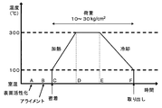
次に、図2を参照して、基板接合プロセスの一例について説明する。
本実施形態に係る基板接合プロセスは、例えば、真空中において、第1の積層体20および第2の積層体40を重ね合わせた後、加熱して接合する。図2は、その過程における処理温度の時間変化を模式的に示している。
Next, an example of the substrate bonding process will be described with reference to FIG.
In the substrate bonding process according to the present embodiment, for example, the first stacked
まず、第1の積層体20および第2の積層体40を、図示しない真空容器の内部に載置し真空容器内を低圧状態にする。
次に、例えば、第1の積層体20と第2の積層体40とを重ね合わせる前に、表面の活性化を行うことができる。(表面活性化A)
具体的には、n型GaAs基板10に設けられた第1の金属層15の表面およびp型Si基板30に設けられた第2の金属層35の表面に、例えば、アルゴン(Ar)イオンビームを照射して、不要な酸化膜及び有機物などを除去する。また、第1の金属層15の表面および第2の金属層35の表面をプラズマ雰囲気に晒しても良い。
また、表面活性化を行わず、第1の積層体20と第2の積層体40とを重ね合わせても良い。
First, the 1st laminated
Next, for example, the surface can be activated before the first stacked
Specifically, for example, an argon (Ar) ion beam is applied to the surface of the
Further, the first
続いて、第1の金属層15の表面と第2の金属層35の表面とを接触させて、第1の積層体20と第2の積層体40とを重ね合わせる。(アライメントB)
具体的には、第1の金属層15の表面と第2の金属層35の表面とを対向させて配置し、n型GaAs基板10およびp型Si基板30の劈開方向を一致させる。さらに、いずれかの基板を回転させて、それぞれの劈開方向の間の角度を所定の角度だけずらす。そして、第1の金属層15と第2の金属層35とを接触させて、第1の積層体20と第2の積層体40とを重ね合わせる。
Subsequently, the surface of the
Specifically, the surface of the
次に、第1の積層体20と第2の積層体40との間に加重を加えて密着させる。(密着C)
第1の積層体20と第2の積層体40とを密着させる温度は、100℃以下であることが望ましい。これにより、例えば、貼り合わせた基板を室温に戻した時に、n型GaAs基板10とp型Si基板30との間の熱膨張率の違いにより発生する反りを小さくすることができる。
Next, a load is applied between the first
The temperature at which the first
第1の積層体20と第2の積層体40との間に加えられる加重は、10kg/cm2以上、30kg/cm2以下とすることができる。第1の金属層15の表面と第2の金属層35の表面とが全体的に密着した状態とするためには、例えば、10kg/cm2以上の加重を加えることが望ましい。さらに、第1の積層体20および第2の積層体40に割れやクラックが発生しないように、30kg/cm2以下の加重とすることが望ましい。
The load applied between the
例えば、劈開方向を一致させて重ね合わせたn型GaAs基板10とp型Si基板30との間に加えることができる加重の最大値は、約20kg/cm2である。一方、両者の劈開方向を1°以上ずらして重ね合わせると、30kg/cm2までの加重を加えることが可能となる。
For example, the maximum value of the weight that can be applied between the n-
続いて、重ね合わせた状態の第1の積層体20および第2の積層体40を、加重を加えたまま加熱して、所定の温度に昇温させる(C→D)。
Subsequently, the first
例えば、第1の金属層15および第2の金属層35がAuを含む金属の場合、250℃以上の温度に加熱する。第1の金属層15と第2の金属層との間に、ボイド等の欠陥が生じないように接合させるためには、250℃以上の温度に昇温させることが望ましいからである。
For example, when the
一方、n型GaAs基板10とp型Si基板30との間の熱膨張率の差に起因する応力により、第1の積層体20および第2の積層体40に割れやクラックが発生しないように350℃以下の温度に保持することが望ましい。
On the other hand, the first
続いて、重ね合わせた状態の第1の積層体20および第2の積層体40を、所定の温度に一定時間保持した後、100℃以下の温度に冷却して真空容器から取り出す。(D→E→取り出しF)
この間、100℃以下の温度に降温されるまで、重ね合わせた第1の積層体20および第2の積層体40に所定の加重を加えた状態を保持する。
Subsequently, the first
In the meantime, until the temperature is lowered to 100 ° C. or lower, a state in which a predetermined load is applied to the stacked first
上記の基板接合プロセスにおいて、例えば、第1の金属層15の表面および第2の金属層35の表面にArイオンビームを照射すると、金属表面に原子の活性な結合手を露出することができる。これにより、第1の金属層15の表面および第2の金属層35の表面の金属原子を結合させるために必要なエネルギーを低減できる。すなわち、Arイオンビームを照射しない場合よりも低温においても接合が可能となる。例えば、表面活性化した後、超高真空の状態で接合プロセスを実施すると、常温で基板を接合できる場合がある。
In the above-described substrate bonding process, for example, when the surface of the
続いて、図1(d)に示すように、上記の基板接合プロセスにより第2の積層体40に接合された第1の積層体20から、機械的研磨法及び溶液エッチング法の少なくとも一方を用いて、n型GaAs基板10を除去する。この場合、n型GaAs基板10を完全に除去しても良いが、一部を残してもよい。
さらに、n型GaAs基板10を除去した半導体層12の表面48にn電極を形成し、p型Si基板30の裏面49にp電極を形成することにより、半導体発光素子を完成させることができる。
Subsequently, as shown in FIG. 1D, at least one of a mechanical polishing method and a solution etching method is used from the first
Further, an n-electrode is formed on the
さらに、別の実施形態として、第1の基板をサファイア基板として、半導体層を窒化物半導体を用いて形成することもできる。例えば、サファイア基板上に、MOCVD法を用いてn型GaN層/発光層/p型GaN層を積層した半導体層を有する第1の積層体を設けることができる。発光層は、InxGa1−xN層(0<x<1)とAlyGa1−yN層(0≦y<1)を交互に積層したMQW層(Multi-Quantum Well)を含むことができる。 Furthermore, as another embodiment, the first substrate can be a sapphire substrate, and the semiconductor layer can be formed using a nitride semiconductor. For example, a first stacked body having a semiconductor layer in which an n-type GaN layer / a light-emitting layer / a p-type GaN layer are stacked using a MOCVD method can be provided on a sapphire substrate. The light emitting layer includes an MQW layer (Multi-Quantum Well) in which an In x Ga 1-x N layer (0 <x <1) and an Al y Ga 1-y N layer (0 ≦ y <1) are alternately stacked. be able to.
さらに、図1(d)に示す第1の基板を除去する工程では。例えば、サファイア基板側から、波長355nmのレーザ光を照射し、サファイア基板とn型GaN層との界面近傍のGaNを溶融してサファイア基板を剥離するレーザリフトオフ法を用いることができる。 Further, in the step of removing the first substrate shown in FIG. For example, a laser lift-off method in which laser light having a wavelength of 355 nm is irradiated from the sapphire substrate side, GaN in the vicinity of the interface between the sapphire substrate and the n-type GaN layer is melted, and the sapphire substrate is peeled off can be used.
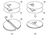
次に、図3を参照して本実施形態に係る半導体発光素子の製造方法の作用効果を説明する。図3(a)は、比較例に係る製造方法の作用を示す模式図であり、図3(b)は、本実施形態に係る製造方法の作用効果を示す模式図である。 Next, the function and effect of the method for manufacturing a semiconductor light emitting device according to this embodiment will be described with reference to FIG. Fig.3 (a) is a schematic diagram which shows the effect | action of the manufacturing method which concerns on a comparative example, FIG.3 (b) is a schematic diagram which shows the effect of the manufacturing method which concerns on this embodiment.
図3(a)に示す比較例に係る製造方法では、第1の積層体20と第2の積層体40とを、それぞれの劈開方向20H、40Hを一致させて接合し、貼り合わせ基板50を形成する。第1の積層体20および第2の積層体40は、応力が加わるとそれぞれの劈開方向に沿って割れやすい性質を有している。したがって、比較例のように、第1の積層体20の劈開方向20Hと、第2の積層体40の劈開方向40Hと、を一致させて接合した場合、貼り合わせ基板50は、図3(a)中に示すように、劈開方向20Hおよび劈開方向40Hと共通する劈開方向50Hにおいて割れ易くなる。
In the manufacturing method according to the comparative example shown in FIG. 3A, the first
上記の性質は、貼り合わせ基板50を用いて製作される半導体素子を個々のチップに分割する際に有利である。例えば、GaAsの(100)基板を用いて第1の積層体20を形成し、Siの(100)基板を用いて第2の積層体40を形成した場合、共に劈開方向は〈110〉方向となり、(011)面および(101)面で劈開される性質を有する。したがって、両者の劈開方向を合わせて接合した貼り合わせ基板50は、(011)面および(101)面の直交する劈開面を有するので、方形の半導体素子チップを容易に切り出すことができる利点を有している。このため、2つの基板を接合する場合に、両者の劈開方向を合わせる製造方法が多用されている。
The above property is advantageous when a semiconductor element manufactured using the bonded
しかしながら、2つの基板の劈開方向を一致させ劈開面を共通にするということは、貼り合わせた基板が割れやすいということを意味する。具体的には、前述した基板接合プロセスにおいて、第1の積層体20と第2の積層体40との間に加熱により生じる応力や、接合界面47に存在するの突起などが要因となって局所的に集中する応力などにより、第1の積層体20と第2の積層体40との両方が割れる可能性が高くなる。
However, the fact that the cleavage directions of the two substrates are made coincident and the cleavage plane is made common means that the bonded substrates are easily broken. Specifically, in the substrate bonding process described above, local stress is caused by stress generated by heating between the first
これに対し、図3(b)に示すように、本実施形態に係る製造方法では、第1の積層体20の劈開方向20Hと、第2の積層体40の劈開方向40Hと、をずらして貼り合わせ基板60を形成する。劈開方向がずれて接合されることにより、一方の基板に割れやクラックが発生したとしても、その応力が他方の基板の劈開方向に直接伝わることがなくなる。したがって、図3(a)に示す貼り合わせ基板50よりも貼り合わせ基板60の強度を高くすることができる。
In contrast, as shown in FIG. 3B, in the manufacturing method according to the present embodiment, the
これにより、基板接合プロセスにおいて発生する割れやクラックを抑制することができ、製造歩留りの向上を図ることができる。具体的には、第1の積層体20の劈開方向20Hと第2の積層体40の劈開方向40Hとの間のずれを1°以上とすることが望ましい。
Thereby, the crack and crack which generate | occur | produce in a board | substrate joining process can be suppressed, and the improvement of a manufacturing yield can be aimed at. Specifically, it is desirable that the shift between the
例えば、第2の積層体40のp型Si基板30は第1の積層体20のn型GaAs基板10よりも強度が高く、第1の積層体20の方が第2の積層体40よりも割れ易い。したがって、図3(b)中に示すように、貼り合わせ基板60において、第1の積層体20が劈開方向20Hに沿って割れたとしても、第2の積層体40がこれを支持し定型を保つことができる。これにより、後続する処理を実施して半導体発光素子を製作することも可能となる。
For example, the p-
図4は、図1に続く半導体発光素子の製造工程を示す模式図である。
図4(a)に示す半導体基板40bは、図1(d)に示す工程で、貼り合わせ基板60からn型GaAs基板10が除去され、第2の積層体40の上に半導体層12が移載されたものである。前述したように、半導体基板40bの半導体層12の表面48にn電極が設けられ、p型Si基板30側の裏面49にp電極が設けられて、半導体発光素子が完成する。
FIG. 4 is a schematic view showing the manufacturing process of the semiconductor light emitting device following FIG.
In the
続いて、図4(a)に示すように、半導体基板40bは、例えば、ダイシングブレードを用いて切断することにより、個々の発光素子チップ65に分割される。
図4(b)は、発光素子チップ65の構造を模式的に示している。n型GaAs基板10上に設けられた半導体層12の劈開方向は、n型GaAs基板の劈開方向20Hと同じ方向である。したがって、例えば、ダイシングブレードによる切断方向を、p型Si基板30の劈開方向40Hに合わせたとすれば、p型Si基板30上に移載された半導体層12は、その劈開方向20Hと異なる方向に切断される。
Subsequently, as shown in FIG. 4A, the
FIG. 4B schematically shows the structure of the light emitting
p型Si基板30の劈開方向40Hと半導体層12の劈開方向20Hとの間の角θが大きいと、ダイシングブレードで半導体基板40bを切断する際に、図4(b)中に示すようなチッピング67a、67bが発生する場合がある。これは、ダイシングブレードによって加わる応力によって、劈開方向20Hに沿って半導体層12が割れることによって生じる。例えば、劈開方向のずれ角θが10°よりも大きくなると、チッピングが発生し易くなる。
When the angle θ between the
前述したように、貼り合わせ基板の強度を向上させるために、劈開方向のずれ角θは1°以上であることが望ましい。したがって、第1の積層体20と第2の積層体40とを重ね合わせた状態における第1の積層体20の劈開方向と第2の積層体の劈開方向とのずれθは、1°以上10°以下とすることが望ましい。
As described above, in order to improve the strength of the bonded substrate, the deviation angle θ in the cleavage direction is desirably 1 ° or more. Therefore, the shift θ between the cleavage direction of the
図5は、別の実施態様に係る半導体発光素子の製造方法を模式的に示す斜視図である。
本実施形態に係る半導体発光素子の製造方法では、第2の積層体に半導体層を残して第1の基板を分離する工程と、第2の積層体の劈開方向に沿った分離溝を設けて、半導体層を個々の半導体素子に分離する工程と、分離溝に沿って第2の積層体を切断する工程と、をさらに備える。
FIG. 5 is a perspective view schematically showing a method for manufacturing a semiconductor light emitting device according to another embodiment.
In the method for manufacturing a semiconductor light emitting device according to this embodiment, a step of separating the first substrate leaving a semiconductor layer in the second stacked body and a separation groove along the cleavage direction of the second stacked body are provided. And a step of separating the semiconductor layer into individual semiconductor elements and a step of cutting the second stacked body along the separation groove.
図5に示す半導体基板40cは、前述した半導体基板40bと同様に、第2の積層体40の上に半導体層12が移載されたものである。さらに、半導体層12は、第2の積層体40の劈開方向40Hに沿った方向に設けられた分離溝72によって、個々の発光素子75に素子分離されている。
分離溝72は、例えば、塩素(Cl2)またはフッ素(F)を含んだエッチングガスを用いたRIE(Reactive Ion Etching)法により形成することができる。また、ウエットエッチングを用いて形成することもできる。
The
The
本実施形態に係る製造方法によれば、分離溝72に沿って個々の発光素子75を分割してチップ化することができる。この際、分離溝72と劈開方向40Hとが一致しているので容易に切断することができる。さらに、半導体層12が分離溝72によって分離されているので、分割の際にダイシングブレードに触れることがなく、例えば、チッピング67a、67bが発生することもない。
According to the manufacturing method according to the present embodiment, the individual
すなわち、本実施形態によれば、第1の積層体20の劈開方向20Hと第2の積層体40の劈開方向40Hとの間のずれ角θを10°よりも大きくすることができる。これにより、貼り合わせ基板60の強度をさらに向上させることができる。
That is, according to the present embodiment, the deviation angle θ between the
なお、本実施形態にいても、第1の金属層または第2の金属層には、例えば、AuまたはAu合金を含むことができる。第1の積層体と第2の積層体とは、100℃以下の温度で重ね合わせる。基板接合プロセスは、第1の積層体と第2の積層体を250℃以上、350℃以下の温度範囲に加熱し、さらに冷却する工程を含み、第1の積層体と第2の積層体との間に加えられる加重は、10kg/cm2以上、30kg/cm2以下とすることができる。 Also in this embodiment, the first metal layer or the second metal layer can contain, for example, Au or an Au alloy. The first stacked body and the second stacked body are overlapped at a temperature of 100 ° C. or lower. The substrate bonding process includes a step of heating the first stacked body and the second stacked body to a temperature range of 250 ° C. or higher and 350 ° C. or lower and further cooling the first stacked body and the second stacked body, The load applied during the period can be 10 kg / cm 2 or more and 30 kg / cm 2 or less.
以上、本発明に係る一実施形態を参照して本発明を説明したが、本発明はこれらの実施形態に限定されるものではない。例えば、出願時の技術水準に基づいて、当業者がなし得る設計変更や、材料の変更等、本発明と技術的思想を同じとする実施態様も本発明の技術的範囲に含有される。 As mentioned above, although this invention was demonstrated with reference to one embodiment which concerns on this invention, this invention is not limited to these embodiment. For example, embodiments that have the same technical idea as the present invention, such as design changes and material changes that can be made by those skilled in the art based on the technical level at the time of filing, are also included in the technical scope of the present invention.
10・・・n型GaAs基板、
12・・・半導体層、
13・・・発光層、
15・・・第1の金属層、
20・・・第1の積層体、
20H、40H、50H・・・劈開方向、
25、45・・・主面
30・・・シリコン(Si)基板、
35・・・第2の金属層、
40・・・第2の積層体、
40b、40c・・・半導体基板、
47・・・接合界面、
50、60・・・貼り合わせ基板、
65・・・発光素子チップ、
67a、67b・・・チッピング、
72・・・分離溝、
75・・・発光素子、
θ・・・ずれ角、
10 ... n-type GaAs substrate,
12 ... Semiconductor layer,
13 ... light emitting layer,
15 ... 1st metal layer,
20 ... 1st laminated body,
20H, 40H, 50H ... cleavage direction,
25, 45 ...
35 ... second metal layer,
40 ... second laminate,
40b, 40c ... semiconductor substrate,
47: Bonding interface,
50, 60 ... bonded substrates,
65. Light emitting element chip,
67a, 67b ... chipping,
72 ... separation groove,
75. Light emitting element,
θ ・ ・ ・ shift angle,
Claims (5)
前記第1の積層体の劈開方向と前記第2の積層体の劈開方向とをずらし、前記第1の金属層と前記第2の金属層とを接触させて重ね合わせる工程と、
前記第1の積層体と前記第2の積層体との間に加重を加えた状態で昇温し、前記第1の積層体と前記第2の積層体とを貼り合わせる工程と、
を備えたことを特徴とする半導体発光素子の製造方法。 A method for manufacturing a semiconductor light-emitting element, in which a first stacked body having a first substrate, a semiconductor layer and a first metal layer, and a second stacked body having a second substrate and a second metal layer are bonded together Because
Shifting the cleavage direction of the first laminate and the cleavage direction of the second laminate, and bringing the first metal layer and the second metal layer into contact with each other;
Raising the temperature in a state where a load is applied between the first laminate and the second laminate, and bonding the first laminate and the second laminate;
A method of manufacturing a semiconductor light emitting device, comprising:
Priority Applications (5)
| Application Number | Priority Date | Filing Date | Title |
|---|---|---|---|
| JP2010063288A JP2011198962A (en) | 2010-03-18 | 2010-03-18 | Method for manufacturing semiconductor light emitting element |
| US12/956,245 US20110229997A1 (en) | 2010-03-18 | 2010-11-30 | Method for manufacturing semiconductor light emitting device |
| EP10195103A EP2367209A2 (en) | 2010-03-18 | 2010-12-15 | Method for manufacturing semiconductor light emitting device |
| TW100105421A TW201214746A (en) | 2010-03-18 | 2011-02-18 | Method for manufacturing semiconductor light emitting device |
| CN2011100669676A CN102194933A (en) | 2010-03-18 | 2011-03-04 | Method for manufacturing semiconductor light emitting device |
Applications Claiming Priority (1)
| Application Number | Priority Date | Filing Date | Title |
|---|---|---|---|
| JP2010063288A JP2011198962A (en) | 2010-03-18 | 2010-03-18 | Method for manufacturing semiconductor light emitting element |
Publications (2)
| Publication Number | Publication Date |
|---|---|
| JP2011198962A true JP2011198962A (en) | 2011-10-06 |
| JP2011198962A5 JP2011198962A5 (en) | 2012-03-22 |
Family
ID=44202051
Family Applications (1)
| Application Number | Title | Priority Date | Filing Date |
|---|---|---|---|
| JP2010063288A Pending JP2011198962A (en) | 2010-03-18 | 2010-03-18 | Method for manufacturing semiconductor light emitting element |
Country Status (5)
| Country | Link |
|---|---|
| US (1) | US20110229997A1 (en) |
| EP (1) | EP2367209A2 (en) |
| JP (1) | JP2011198962A (en) |
| CN (1) | CN102194933A (en) |
| TW (1) | TW201214746A (en) |
Cited By (1)
| Publication number | Priority date | Publication date | Assignee | Title |
|---|---|---|---|---|
| US9865786B2 (en) | 2012-06-22 | 2018-01-09 | Soitec | Method of manufacturing structures of LEDs or solar cells |
Families Citing this family (4)
| Publication number | Priority date | Publication date | Assignee | Title |
|---|---|---|---|---|
| KR100599012B1 (en) * | 2005-06-29 | 2006-07-12 | 서울옵토디바이스주식회사 | Light emitting diode having a thermal conductive substrate and method of fabricating the same |
| JP2010109015A (en) * | 2008-10-28 | 2010-05-13 | Panasonic Electric Works Co Ltd | Method of manufacturing semiconductor light-emitting element |
| TWI478384B (en) | 2011-12-28 | 2015-03-21 | Toshiba Kk | Semiconductor light emitting element and manufacturing method thereof |
| JP7347197B2 (en) * | 2019-12-19 | 2023-09-20 | トヨタ自動車株式会社 | Manufacturing method and manufacturing device for rotating electrical machine core |
Citations (5)
| Publication number | Priority date | Publication date | Assignee | Title |
|---|---|---|---|---|
| JPH06296040A (en) * | 1993-02-10 | 1994-10-21 | Sharp Corp | Manufacture of light-emitting diode |
| JPH09320912A (en) * | 1996-06-03 | 1997-12-12 | Nec Corp | Semiconductor substrate and manufacture thereof |
| WO2003049189A1 (en) * | 2001-12-04 | 2003-06-12 | Shin-Etsu Handotai Co.,Ltd. | Pasted wafer and method for producing pasted wafer |
| JP2007194247A (en) * | 2006-01-17 | 2007-08-02 | Sony Corp | Semiconductor light emitting device and its fabrication process |
| JP2009040639A (en) * | 2007-08-09 | 2009-02-26 | Mitsubishi Electric Corp | Semiconductor wafer device |
Family Cites Families (9)
| Publication number | Priority date | Publication date | Assignee | Title |
|---|---|---|---|---|
| DE60042187D1 (en) * | 1999-06-09 | 2009-06-25 | Toshiba Kawasaki Kk | Bond-type semiconductor substrate, semiconductor light-emitting device, and manufacturing method |
| US6333208B1 (en) * | 1999-07-13 | 2001-12-25 | Li Chiung-Tung | Robust manufacturing method for making a III-V compound semiconductor device by misaligned wafer bonding |
| JP2002134374A (en) * | 2000-10-25 | 2002-05-10 | Mitsubishi Electric Corp | Semiconductor wafer and its manufacturing method and device |
| WO2005091391A1 (en) | 2004-03-18 | 2005-09-29 | Showa Denko K.K. | Group iii nitride semiconductor light-emitting device and method of producing the same |
| JP4935136B2 (en) * | 2006-03-22 | 2012-05-23 | パナソニック株式会社 | Light emitting element |
| US7795054B2 (en) * | 2006-12-08 | 2010-09-14 | Samsung Led Co., Ltd. | Vertical structure LED device and method of manufacturing the same |
| JP4471003B2 (en) * | 2008-01-23 | 2010-06-02 | セイコーエプソン株式会社 | Method for forming joined body |
| JP4492733B2 (en) * | 2008-05-27 | 2010-06-30 | ソニー株式会社 | LIGHT EMITTING DEVICE AND LIGHT EMITTING DEVICE MANUFACTURING METHOD |
| JP2010186829A (en) * | 2009-02-10 | 2010-08-26 | Toshiba Corp | Method for manufacturing light emitting element |
-
2010
- 2010-03-18 JP JP2010063288A patent/JP2011198962A/en active Pending
- 2010-11-30 US US12/956,245 patent/US20110229997A1/en not_active Abandoned
- 2010-12-15 EP EP10195103A patent/EP2367209A2/en not_active Withdrawn
-
2011
- 2011-02-18 TW TW100105421A patent/TW201214746A/en unknown
- 2011-03-04 CN CN2011100669676A patent/CN102194933A/en active Pending
Patent Citations (5)
| Publication number | Priority date | Publication date | Assignee | Title |
|---|---|---|---|---|
| JPH06296040A (en) * | 1993-02-10 | 1994-10-21 | Sharp Corp | Manufacture of light-emitting diode |
| JPH09320912A (en) * | 1996-06-03 | 1997-12-12 | Nec Corp | Semiconductor substrate and manufacture thereof |
| WO2003049189A1 (en) * | 2001-12-04 | 2003-06-12 | Shin-Etsu Handotai Co.,Ltd. | Pasted wafer and method for producing pasted wafer |
| JP2007194247A (en) * | 2006-01-17 | 2007-08-02 | Sony Corp | Semiconductor light emitting device and its fabrication process |
| JP2009040639A (en) * | 2007-08-09 | 2009-02-26 | Mitsubishi Electric Corp | Semiconductor wafer device |
Cited By (1)
| Publication number | Priority date | Publication date | Assignee | Title |
|---|---|---|---|---|
| US9865786B2 (en) | 2012-06-22 | 2018-01-09 | Soitec | Method of manufacturing structures of LEDs or solar cells |
Also Published As
| Publication number | Publication date |
|---|---|
| US20110229997A1 (en) | 2011-09-22 |
| TW201214746A (en) | 2012-04-01 |
| CN102194933A (en) | 2011-09-21 |
| EP2367209A2 (en) | 2011-09-21 |
Similar Documents
| Publication | Publication Date | Title |
|---|---|---|
| US8426884B2 (en) | Light emitting diode with supporting substrate side electrodes and wiring structures | |
| JP4857596B2 (en) | Method for manufacturing light emitting device | |
| EP2063469B1 (en) | Method of manufacturing vertical light emitting diode | |
| JP3784785B2 (en) | Manufacturing method of vertical structure gallium nitride based light emitting diode | |
| US7554124B2 (en) | Nitride-based compound semiconductor light emitting device, structural unit thereof, and fabricating method thereof | |
| US20090315045A1 (en) | Integrated semiconductor light emitting device and method for manufacturing same | |
| JP4817673B2 (en) | Nitride semiconductor device fabrication method | |
| JP2013070111A (en) | Semiconductor light-emitting device | |
| JP4584785B2 (en) | Manufacturing method of semiconductor light emitting device | |
| JP2010186829A (en) | Method for manufacturing light emitting element | |
| JP2009105123A (en) | Light-emitting diode, and manufacturing method thereof | |
| JP5992702B2 (en) | Semiconductor light emitting device, vehicle lamp, and method for manufacturing semiconductor light emitting device | |
| KR100916366B1 (en) | Supporting substrates for semiconductor light emitting device and method of manufacturing vertical structured semiconductor light emitting device using the supporting substrates | |
| JP2007324585A (en) | Semiconductor light-emitting element | |
| JP2011198962A (en) | Method for manufacturing semiconductor light emitting element | |
| CN102646763A (en) | Manufacturing method of nitride semiconductor light emitting elements | |
| JP2007324581A (en) | Integrated semiconductor light-emitting device, and manufacturing method thereof | |
| JP2008117824A (en) | Method of manufacturing nitride-based semiconductor element | |
| US8618562B2 (en) | Light emitting device and method for manufacturing same | |
| JP2007324586A (en) | Manufacturing method of semiconductor light-emitting element | |
| JP6245791B2 (en) | Vertical nitride semiconductor device and manufacturing method thereof | |
| JP5605033B2 (en) | Light emitting diode manufacturing method, cutting method, and light emitting diode | |
| KR20090115902A (en) | Fabrication of vertical structured light emitting diodes using group 3 nitride-based semiconductors and its related methods | |
| JP2007324583A (en) | Integrated semiconductor light-emitting device, and manufacturing method thereof | |
| JP5940315B2 (en) | Semiconductor light emitting device and manufacturing method thereof |
Legal Events
| Date | Code | Title | Description |
|---|---|---|---|
| A521 | Written amendment |
Free format text: JAPANESE INTERMEDIATE CODE: A523 Effective date: 20120206 |
|
| A621 | Written request for application examination |
Free format text: JAPANESE INTERMEDIATE CODE: A621 Effective date: 20120206 |
|
| A871 | Explanation of circumstances concerning accelerated examination |
Free format text: JAPANESE INTERMEDIATE CODE: A871 Effective date: 20120206 |
|
| A975 | Report on accelerated examination |
Free format text: JAPANESE INTERMEDIATE CODE: A971005 Effective date: 20120328 |
|
| A131 | Notification of reasons for refusal |
Free format text: JAPANESE INTERMEDIATE CODE: A131 Effective date: 20120528 |
|
| A02 | Decision of refusal |
Free format text: JAPANESE INTERMEDIATE CODE: A02 Effective date: 20120928 |