EP2367209A2 - Method for manufacturing semiconductor light emitting device - Google Patents
Method for manufacturing semiconductor light emitting device Download PDFInfo
- Publication number
- EP2367209A2 EP2367209A2 EP10195103A EP10195103A EP2367209A2 EP 2367209 A2 EP2367209 A2 EP 2367209A2 EP 10195103 A EP10195103 A EP 10195103A EP 10195103 A EP10195103 A EP 10195103A EP 2367209 A2 EP2367209 A2 EP 2367209A2
- Authority
- EP
- European Patent Office
- Prior art keywords
- stacked body
- substrate
- metal layer
- cleavage direction
- semiconductor
- Prior art date
- Legal status (The legal status is an assumption and is not a legal conclusion. Google has not performed a legal analysis and makes no representation as to the accuracy of the status listed.)
- Withdrawn
Links
- 239000004065 semiconductor Substances 0.000 title claims abstract description 67
- 238000000034 method Methods 0.000 title claims abstract description 49
- 238000004519 manufacturing process Methods 0.000 title claims abstract description 26
- 239000000758 substrate Substances 0.000 claims abstract description 112
- 239000002184 metal Substances 0.000 claims abstract description 65
- 229910052751 metal Inorganic materials 0.000 claims abstract description 65
- 238000003776 cleavage reaction Methods 0.000 claims abstract description 55
- 230000007017 scission Effects 0.000 claims abstract description 55
- 238000003825 pressing Methods 0.000 claims abstract description 9
- 229910001218 Gallium arsenide Inorganic materials 0.000 claims description 21
- 239000010931 gold Substances 0.000 claims description 10
- 238000005520 cutting process Methods 0.000 claims description 6
- 229910052594 sapphire Inorganic materials 0.000 claims description 6
- 239000010980 sapphire Substances 0.000 claims description 6
- 229910052737 gold Inorganic materials 0.000 claims description 5
- 238000010884 ion-beam technique Methods 0.000 claims description 4
- 230000001678 irradiating effect Effects 0.000 claims description 3
- XUIMIQQOPSSXEZ-UHFFFAOYSA-N Silicon Chemical compound [Si] XUIMIQQOPSSXEZ-UHFFFAOYSA-N 0.000 claims description 2
- PCHJSUWPFVWCPO-UHFFFAOYSA-N gold Chemical compound [Au] PCHJSUWPFVWCPO-UHFFFAOYSA-N 0.000 claims description 2
- 229910052710 silicon Inorganic materials 0.000 claims description 2
- 239000010703 silicon Substances 0.000 claims description 2
- 230000008569 process Effects 0.000 description 19
- 230000004913 activation Effects 0.000 description 4
- 230000000694 effects Effects 0.000 description 4
- 230000000052 comparative effect Effects 0.000 description 3
- 150000004767 nitrides Chemical class 0.000 description 3
- XKRFYHLGVUSROY-UHFFFAOYSA-N Argon Chemical compound [Ar] XKRFYHLGVUSROY-UHFFFAOYSA-N 0.000 description 2
- 239000010949 copper Substances 0.000 description 2
- 239000013078 crystal Substances 0.000 description 2
- 238000005530 etching Methods 0.000 description 2
- 150000002739 metals Chemical class 0.000 description 2
- 238000001451 molecular beam epitaxy Methods 0.000 description 2
- 238000001020 plasma etching Methods 0.000 description 2
- 229910001020 Au alloy Inorganic materials 0.000 description 1
- -1 Au such as AuIn Chemical class 0.000 description 1
- KZBUYRJDOAKODT-UHFFFAOYSA-N Chlorine Chemical compound ClCl KZBUYRJDOAKODT-UHFFFAOYSA-N 0.000 description 1
- ZAMOUSCENKQFHK-UHFFFAOYSA-N Chlorine atom Chemical compound [Cl] ZAMOUSCENKQFHK-UHFFFAOYSA-N 0.000 description 1
- RYGMFSIKBFXOCR-UHFFFAOYSA-N Copper Chemical compound [Cu] RYGMFSIKBFXOCR-UHFFFAOYSA-N 0.000 description 1
- PXGOKWXKJXAPGV-UHFFFAOYSA-N Fluorine Chemical compound FF PXGOKWXKJXAPGV-UHFFFAOYSA-N 0.000 description 1
- 229910045601 alloy Inorganic materials 0.000 description 1
- 239000000956 alloy Substances 0.000 description 1
- 229910052782 aluminium Inorganic materials 0.000 description 1
- XAGFODPZIPBFFR-UHFFFAOYSA-N aluminium Chemical compound [Al] XAGFODPZIPBFFR-UHFFFAOYSA-N 0.000 description 1
- 229910052786 argon Inorganic materials 0.000 description 1
- 230000004888 barrier function Effects 0.000 description 1
- 230000008901 benefit Effects 0.000 description 1
- 230000008859 change Effects 0.000 description 1
- 238000005229 chemical vapour deposition Methods 0.000 description 1
- 239000000460 chlorine Substances 0.000 description 1
- 229910052801 chlorine Inorganic materials 0.000 description 1
- 150000001875 compounds Chemical class 0.000 description 1
- 238000001816 cooling Methods 0.000 description 1
- 229910052802 copper Inorganic materials 0.000 description 1
- 230000007547 defect Effects 0.000 description 1
- 229910052731 fluorine Inorganic materials 0.000 description 1
- 239000011737 fluorine Substances 0.000 description 1
- 239000007789 gas Substances 0.000 description 1
- 238000010438 heat treatment Methods 0.000 description 1
- 238000012986 modification Methods 0.000 description 1
- 230000004048 modification Effects 0.000 description 1
- 238000005498 polishing Methods 0.000 description 1
- 229910000679 solder Inorganic materials 0.000 description 1
- 239000000126 substance Substances 0.000 description 1
- 238000006467 substitution reaction Methods 0.000 description 1
- 230000002123 temporal effect Effects 0.000 description 1
- WFKWXMTUELFFGS-UHFFFAOYSA-N tungsten Chemical compound [W] WFKWXMTUELFFGS-UHFFFAOYSA-N 0.000 description 1
- 229910052721 tungsten Inorganic materials 0.000 description 1
- 239000010937 tungsten Substances 0.000 description 1
- 238000007740 vapor deposition Methods 0.000 description 1
- 238000001039 wet etching Methods 0.000 description 1
Images

Classifications
-
- H—ELECTRICITY
- H01—ELECTRIC ELEMENTS
- H01L—SEMICONDUCTOR DEVICES NOT COVERED BY CLASS H10
- H01L33/00—Semiconductor devices having potential barriers specially adapted for light emission; Processes or apparatus specially adapted for the manufacture or treatment thereof or of parts thereof; Details thereof
- H01L33/005—Processes
- H01L33/0095—Post-treatment of devices, e.g. annealing, recrystallisation or short-circuit elimination
-
- H—ELECTRICITY
- H01—ELECTRIC ELEMENTS
- H01L—SEMICONDUCTOR DEVICES NOT COVERED BY CLASS H10
- H01L33/00—Semiconductor devices having potential barriers specially adapted for light emission; Processes or apparatus specially adapted for the manufacture or treatment thereof or of parts thereof; Details thereof
- H01L33/005—Processes
- H01L33/0093—Wafer bonding; Removal of the growth substrate
Definitions
- Embodiments described herein relate generally to a method for manufacturing a semiconductor light emitting device.
- JP-A 2005-303287 discusses increasing the productivity of a Group III nitride semiconductor light emitting device by separating a Group III nitride semiconductor layer from a growth substrate.
- a method for manufacturing a semiconductor light emitting device characterized by bonding a first stacked body to a second stacked body.
- the first stacked body includes a first substrate, a semiconductor layer, and a first metal layer.
- the second stacked body includes a second substrate and a second metal layer.
- the method can include overlaying the first metal layer and the second metal layer by shifting a cleavage direction of the first stacked body from a cleavage direction of the second stacked body and by bringing the first metal layer and the second metal layer into contact.
- the method can include bonding the first stacked body and the second stacked body by increasing a temperature in a state of pressing the first stacked body and the second stacked body into contact.
- a method for manufacturing a semiconductor light emitting device includes a process of overlaying a first stacked body including a first metal layer provided on a first substrate with a second stacked body including a second metal layer provided on a second substrate by shifting a cleavage direction of the first substrate from a cleavage direction of the second substrate and by bringing the first metal layer and the second metal layer into contact.
- the first stacked body includes a semiconductor layer on the first substrate, where the semiconductor layer includes a light emitting layer that radiates light; and the first metal layer is provided on the semiconductor layer.
- the method further includes a process of bonding the first stacked body and the second stacked body by increasing a temperature in a state of pressing the first stacked body and the second stacked body into contact.
- FIGS. 1A to 1D are cross-sectional views of processes schematically illustrating the method for manufacturing the semiconductor light emitting device according to the one embodiment of the invention.
- the first substrate is taken to be an n-type GaAs substrate 10 and the second substrate is taken to be a p-type silicon (Si) substrate 30.
- a semiconductor layer 12 provided on the n-type GaAs substrate 10 includes, for example, an InGaAlP semiconductor.
- FIG. 1A illustrates a cross section of a first stacked body 20 in which the semiconductor layer 12 is provided.
- FIG. 1B illustrates a cross section of a second stacked body 40.
- FIG. 1C is a cross-sectional view illustrating the state of the second stacked body 40 overlaid on the first stacked body 20.
- FIG. 1D is a cross-sectional view illustrating the state in which the semiconductor layer 12 remains on the second stacked body 40 and the n-type GaAs substrate 10 is removed.
- the first stacked body 20 includes the n-type GaAs substrate 10, the semiconductor layer 12 and a first metal layer 15.
- the semiconductor layer 12 is formed by using, for example, MOCVD (Metal Organic Chemical Vapor Deposition) or MBE (Molecular Beam Epitaxy), or the like.
- the second stacked body 40 includes the p-type Si substrate 30 and a second metal layer 35 formed by using vacuum vapor deposition.
- the semiconductor light emitting device can emit visible light in a wavelength range of yellowish-green to red.
- a good crystal can be provided easily because the semiconductor layer 12 is made of an InGaAlP compound crystal and has lattice matching with GaAs.
- the first stacked body 20 is overlaid on the second stacked body 40; and the first metal layer 15 and the second metal layer 35 are brought into contact at a bonding interface 47. Then, a prescribed substrate bonding process is implemented to bond the first stacked body 20 and the second stacked body 40. At this time, the first stacked body 20 and the second stacked body 40 are bonded with a cleavage direction of the first stacked body 20 shifted from a cleavage direction of the second stacked body 40.
- the cleavage direction of the first stacked body 20 matches the cleavage direction of the n-type GaAs substrate 10; and the cleavage direction of the second stacked body 40 matches the cleavage direction of the p-type Si substrate 30. Accordingly, in the case where a major surface 25 of the n-type GaAs substrate 10 is a (100) surface and a major surface 45 of the p-type Si substrate 30 is a (100) surface, the first stacked body 20 and the second stacked body 40 are bonded with the ⁇ 110> direction of the n-type GaAs substrate 10 shifted from the ⁇ 110> direction of the p-type Si substrate 30.
- the first metal layer 15 or the second metal layer 35 may include, for example, gold (Au) and metals including Au such as AuIn, AuSn, etc.
- Au gold
- AuSn gold
- the bonding strength between Au and Au may be increased by the first metal layer 15 and the second metal layer 35 having a multilayered structure of Ti/Pt/Au.
- a solder alloy of InSn and the like also may be used.
- the first metal layer 15 or the second metal layer 35 may include tungsten (W) as a barrier metal.
- the first metal layer and the second metal layer also may be, for example, copper (Cu) or aluminum (Al).
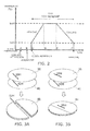
- FIG. 2 schematically illustrates the temporal change of the processing temperature of such a process.
- the first stacked body 20 and the second stacked body 40 are placed in the interior of a not-illustrated vacuum container; and the interior of the vacuum container is brought to a low-pressure state.
- surface activation may be performed prior to overlaying the first stacked body 20 and the second stacked body 40.
- unnecessary oxide films, organic substances, and the like are removed from the surface of the first metal layer and the surface of the second metal layer 35 by, for example, irradiating an argon (Ar) ion beam. Also, the surface of the first metal layer 15 and the surface of the second metal layer 35 may be exposed to a plasma atmosphere.
- Ar argon
- first stacked body 20 and the second stacked body 40 may be overlaid without performing the surface activation.
- the surface of the first metal layer 15 and the surface of the second metal layer 35 are disposed opposing each other; and the cleavage directions of the n-type GaAs substrate 10 and the p-type Si substrate 30 are matched. Further, either of the substrates is rotated to shift the angle between the cleavage directions thereof to a prescribed angle. Then, the first metal layer 15 and the second metal layer 35 are brought into contact to overlay the first stacked body 20 and the second stacked body 40.
- the temperature at which the first stacked body 20 and the second stacked body 40 are closely adhered is not more than 100 °C. Thereby, it is possible to reduce the warp occurring due to differences in the coefficient of thermal expansion between the n-type GaAs substrate 10 and the p-type Si substrate 30, for example, when returning the bonded substrates to room temperature.
- the load applied between the first stacked body 20 and the second stacked body 40 may be not less than 10 kg/cm 2 and not more than 30 kg/cm 2 . It is desirable to apply, for example, a pressing load not less than 10 kg/cm 2 to provide a state in which the surface of the first metal layer 15 and the surface of the second metal layer 35 are entirely and closely adhered. Further, it is desirable for the load to be not more than 30 kg/cm 2 so that breakage and cracks of the first stacked body 20 and the second stacked body 40 do not occur.
- the maximum load of, for example, about 20 kg/cm 2 can be applied between the n-type GaAs substrate 10 and the p-type Si substrate 30 when overlaid with matched cleavage directions.
- a pressing load of up to 30 kg/cm 2 by overlaying with a shifted angle between the two cleavage directions of not less than 1°.
- the first stacked body 20 and the second stacked body 40 are heated in the overlaid state while the load is applied; and the temperature is increased to a prescribed temperature (C to D).
- the first metal layer 15 and the second metal layer 35 are metals including Au
- the first metal layer 15 and the second metal layer 35 are heated to a temperature not less than 250 °C. This is because it is desirable to increase the temperature to not less than 250 °C to bond the first stacked body 20 and the second stacked body 40 such that defects such as voids and the like do not occur between the first metal layer 15 and the second metal layer 35.
- the temperature is desirable to maintain the temperature at not more than 350 °C so that breakage and cracks do not occur in the first stacked body 20 and the second stacked body 40 due to stress caused by differences in the coefficient of thermal expansion between the n-type GaAs substrate 10 and the p-type Si substrate 30.
- the first stacked body 20 and the second stacked body 40 are cooled to a temperature of 100 °C or less and removed from the vacuum container. (D to E to removal F)
- the overlaid first stacked body 20 and second stacked body 40 are maintained in the state of the applied prescribed load until the temperature is reduced to 100 °C or less.
- the n-type GaAs substrate 10 is removed from the first stacked body 20 bonded to the second stacked body 40 by using at least one selected from mechanical polishing and solution-based etching.
- the n-type GaAs substrate 10 may be completely removed; or a portion thereof may remain.
- the semiconductor light emitting device is completed by forming an n-electrode on a front face 48 of the semiconductor layer 12 from which the n-type GaAs substrate 10 is removed and by forming a p-electrode on a back face 49 of the p-type Si substrate 30.
- the first substrate may be a sapphire substrate; and the semiconductor layer may be formed using a nitride semiconductor.
- the first stacked body including a semiconductor layer, in which an n-type GaN layer/light emitting layer/p-type GaN layer are stacked, may be provided by MOCVD on the sapphire substrate.
- the light emitting layer may include a MQW (Multi-Quantum Well) layer in which an In x Ga 1-x N layer (0 ⁇ x ⁇ 1) and an Al y Ga 1-y N layer (0 ⁇ y ⁇ 1) are alternately stacked.
- MQW Multi-Quantum Well
- laser lift-off may be used in which laser light having a wavelength of 355 nm is irradiated from the sapphire substrate side; the GaN is decomposed in a portion proximal to the interface between the sapphire substrate and the n-type GaN layer; and the sapphire substrate is peeled.
- FIG. 3A is a schematic view illustrating the effects of a manufacturing method according to a comparative example
- FIG. 3B is a schematic view illustrating the operations and effects of the manufacturing method according to this embodiment.
- the first stacked body 20 and the second stacked body 40 are bonded with cleavage directions 20H and 40H thereof matched to form a bonded substrate 50.
- the first stacked body 20 and the second stacked body 40 have the property of being easily broken along the cleavage directions thereof when stress is applied. Accordingly, in the case where the cleavage direction 20H of the first stacked body 20 is matched to the cleavage direction 40H of the second stacked body 40 as in the comparative example, the bonded substrate 50 is easily broken along a cleavage direction 50H common to the cleavage direction 20H and the cleavage direction 40H as illustrated in FIG. 3A .
- the property recited above is advantageous when subdividing the semiconductor devices constructed using the bonded substrate 50 into individual chips.
- the cleavage direction of both is the ⁇ 110> direction; and the (011) surface and the (101) surface have cleaving properties.
- the bonded substrate 50 bonded with the two matched cleavage directions has the advantage that rectangular semiconductor device chips can be cut out easily because the bonded substrate 50 has orthogonal cleaving surfaces of the (011) surface and the (101) surface. Therefore, when bonding two substrates, manufacturing methods are often used, where the two cleavage directions match each other.
- matching the cleavage directions of two substrates to have a common cleaving surface means that the bonded substrates are easily broken.
- both the first stacked body 20 and the second stacked body 40 may break due to stress occurring between the first stacked body 20 and the second stacked body 40 due to heating, locally concentrated stress due to protrusions and the like existing at the bonding interface 47, etc.
- a substrate 60 is formed by bonding in which the cleavage direction 20H of the first stacked body 20 and the cleavage direction 40H of the second stacked body 40 are shifted.
- the stress thereof is not transmitted directly to the cleavage direction of the other substrate. Accordingly, the strength of the bonded substrate 60 can be higher than that of the bonded substrate 50 illustrated in FIG. 3A .
- the shift between the cleavage direction 20H of the first stacked body 20 and the cleavage direction 40H of the second stacked body 40 is not less than 1°.
- the p-type Si substrate 30 of the second stacked body 40 is stronger than the n-type GaAs substrate 10 of the first stacked body 20; and the first stacked body 20 breaks more easily than the second stacked body 40. Accordingly, in the bonded substrate 60 as illustrated in FIG. 3B , the second stacked body 40 can support and maintain the fixed form even in the case where the first stacked body 20 breaks along the cleavage direction 20H. Thereby, it is possible to implement subsequent processing to construct the semiconductor light emitting device.
- FIGS. 4A and 4B are schematic views illustrating the manufacturing processes of the semiconductor light emitting device continuing from FIG. 1D .
- a semiconductor substrate 40b illustrated in FIG. 4A the n-type GaAs substrate 10 has been removed from the bonded substrate 60 in the process illustrated in FIG. 1D , and the semiconductor layer 12 is transferred onto the second stacked body 40.
- an n-electrode is provided on the front face 48 of the semiconductor layer 12 of the semiconductor substrate 40b; a p-electrode is provided on the back face 49 on the p-type Si substrate 30 side; and the semiconductor light emitting device is completed.
- the semiconductor substrate 40b is subdivided into individual light emitting device chips 65 by cutting using, for example, a dicing blade.
- FIG. 4B schematically illustrates the structure of the light emitting device chip 65.
- the cleavage direction of the semiconductor layer 12 provided on the n-type GaAs substrate 10 is the same direction as the cleavage direction 20H of the n-type GaAs substrate 10. Accordingly, for example, if the cutting direction of the dicing blade is matched to the cleavage direction 40H of the p-type Si substrate 30, the semiconductor layer 12 transferred onto the p-type Si substrate 30 is cut in a direction different from the cleavage direction 20H thereof.
- the shifted angle ⁇ of the cleavage direction is not less than 1° to increase the strength of the bonded substrates. Accordingly, it is desirable for the shifted angle ⁇ between the cleavage direction of the first stacked body 20 and the cleavage direction of the second stacked body 40 to be not less than 1° and not more than 10° in the state in which the first stacked body 20 and the second stacked body 40 are overlaid.
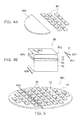
- FIG. 5 is a perspective view schematically illustrating the method for manufacturing the semiconductor light emitting device according to another mode of implementation.
- the method for manufacturing the semiconductor light emitting device further includes: a process of separating the first substrate while leaving the semiconductor layer on the second stacked body; a process of providing a dicing groove along the cleavage direction of the second stacked body to separate the semiconductor layer into individual semiconductor devices; and a process of cutting the second stacked body along the dicing groove.
- the semiconductor layer 12 is transferred onto the second stacked body 40 in a semiconductor substrate 40c illustrated in FIG. 5 . Further, the semiconductor layer 12 is separated into individual light emitting devices 75 by a dicing groove 72 provided in the direction along the cleavage direction 40H of the second stacked body 40.
- the dicing groove 72 can be made by, for example, RIE (Reactive Ion Etching) using an etching gas including chlorine (Cl 2 ) or fluorine (F). Wet etching also can be used.
- the individual light emitting devices 75 can be subdivided along the dicing groove 72 into chips.
- the cutting is easy because the dicing groove 72 and the cleavage direction 40H are matched to each other.
- the semiconductor layer 12 is separated by the dicing groove 72, there is no contact with the dicing blade when subdividing and, for example, the chipping 67a and 67b does not occur.
- the shifted angle ⁇ between the cleavage direction 20H of the first stacked body 20 and the cleavage direction 40H of the second stacked body 40 can be greater than 10°.
- the first metal layer or the second metal layer may include, for example, Au or Au alloy.
- the first stacked body and the second stacked body are overlaid at a temperature not more than 100 °C.
- the substrate bonding process heats the first stacked body and the second stacked body to a temperature range of not less than 250 °C and not more than 350 °C and further includes a cooling process; and the pressing load applied between the first stacked body and the second stacked body can be not less than 10 kg/cm 2 and not more than 30 kg/cm 2 .
Landscapes
- Engineering & Computer Science (AREA)
- Manufacturing & Machinery (AREA)
- Computer Hardware Design (AREA)
- Microelectronics & Electronic Packaging (AREA)
- Power Engineering (AREA)
- Led Devices (AREA)
- Semiconductor Lasers (AREA)
Abstract
A method for manufacturing a semiconductor light emitting device characterized by bonding a first stacked body (20) to a second stacked body (40) is disclosed. The first stacked body includes a first substrate (10), a semiconductor layer (12), and a first metal layer (15). The second stacked body includes a second substrate (30) and a second metal layer (35). The method includes overlaying the first metal layer and the second metal layer by shifting a cleavage direction of the first stacked body from a cleavage direction of the second stacked body. The method includes bonding the first stacked body and the second stacked body by increasing a temperature in a state of pressing the first stacked body and the second stacked body into contact.


Description
- Embodiments described herein relate generally to a method for manufacturing a semiconductor light emitting device.
- Manufacturing methods in which a semiconductor layer including a light emitting layer is separated from a growth substrate and transferred onto another substrate have been used for semiconductor light emitting devices such as light emitting diodes (LEDs). For example,
JP-A 2005-303287 - However, there are cases in which breakage and cracks of the substrate occur when the semiconductor layer is transferred onto the different substrate. Therefore, there is a need for a manufacturing method that can prevent breakage and cracks of the substrate.
-
-
FIGS. 1A to 1D are cross-sectional views of processes schematically illustrating a method for manufacturing a semiconductor light emitting device according to an embodiment; -
FIG. 2 is a schematic view describing a substrate bonding process performed in the manufacturing process of the semiconductor light emitting device according to the embodiment; -
FIGS. 3A and 3B are schematic views describing operations and effects of the method for manufacturing the semiconductor device according to the embodiment; -
FIGS. 4A and 4B are schematic views illustrating the manufacturing processes of the semiconductor light emitting device continuing fromFIG. 1D ; and -
FIG. 5 is a perspective view schematically illustrating the method for manufacturing the semiconductor light emitting device according to another embodiment. - In one embodiment, a method for manufacturing a semiconductor light emitting device characterized by bonding a first stacked body to a second stacked body is disclosed. The first stacked body includes a first substrate, a semiconductor layer, and a first metal layer. The second stacked body includes a second substrate and a second metal layer. The method can include overlaying the first metal layer and the second metal layer by shifting a cleavage direction of the first stacked body from a cleavage direction of the second stacked body and by bringing the first metal layer and the second metal layer into contact. The method can include bonding the first stacked body and the second stacked body by increasing a temperature in a state of pressing the first stacked body and the second stacked body into contact.
- Embodiments of the invention will now be described with reference to the drawings. In the embodiments hereinbelow, similar portions in the drawings are marked with like numerals and a detailed description thereof is omitted as appropriate; and different portions are described as appropriate.
- A method for manufacturing a semiconductor light emitting device according to one embodiment of the invention includes a process of overlaying a first stacked body including a first metal layer provided on a first substrate with a second stacked body including a second metal layer provided on a second substrate by shifting a cleavage direction of the first substrate from a cleavage direction of the second substrate and by bringing the first metal layer and the second metal layer into contact. The first stacked body includes a semiconductor layer on the first substrate, where the semiconductor layer includes a light emitting layer that radiates light; and the first metal layer is provided on the semiconductor layer.
- The method further includes a process of bonding the first stacked body and the second stacked body by increasing a temperature in a state of pressing the first stacked body and the second stacked body into contact.
-
FIGS. 1A to 1D are cross-sectional views of processes schematically illustrating the method for manufacturing the semiconductor light emitting device according to the one embodiment of the invention. In the description of the manufacturing method according to this embodiment, for example, the first substrate is taken to be an n-type GaAs substrate 10 and the second substrate is taken to be a p-type silicon (Si)substrate 30. Asemiconductor layer 12 provided on the n-type GaAs substrate 10 includes, for example, an InGaAlP semiconductor. -
FIG. 1A illustrates a cross section of a first stackedbody 20 in which thesemiconductor layer 12 is provided.FIG. 1B illustrates a cross section of a second stackedbody 40.FIG. 1C is a cross-sectional view illustrating the state of the second stackedbody 40 overlaid on the first stackedbody 20.FIG. 1D is a cross-sectional view illustrating the state in which thesemiconductor layer 12 remains on the secondstacked body 40 and the n-type GaAs substrate 10 is removed. - As illustrated in
FIG. 1A , the first stackedbody 20 includes the n-type GaAs substrate 10, thesemiconductor layer 12 and afirst metal layer 15. Thesemiconductor layer 12 is formed by using, for example, MOCVD (Metal Organic Chemical Vapor Deposition) or MBE (Molecular Beam Epitaxy), or the like. - On the other hand, as illustrated in
FIG. 1B , the second stackedbody 40 includes the p-type Si substrate 30 and asecond metal layer 35 formed by using vacuum vapor deposition. - In the case where a
light emitting layer 13 included in thesemiconductor layer 12 is an IrtGaAlP semiconductor, the semiconductor light emitting device can emit visible light in a wavelength range of yellowish-green to red. A good crystal can be provided easily because thesemiconductor layer 12 is made of an InGaAlP compound crystal and has lattice matching with GaAs. - Then, as illustrated in
FIG. 1C , the first stackedbody 20 is overlaid on the second stackedbody 40; and thefirst metal layer 15 and thesecond metal layer 35 are brought into contact at abonding interface 47. Then, a prescribed substrate bonding process is implemented to bond the first stackedbody 20 and the second stackedbody 40. At this time, the first stackedbody 20 and the second stackedbody 40 are bonded with a cleavage direction of the first stackedbody 20 shifted from a cleavage direction of the second stackedbody 40. - For example, the cleavage direction of the first stacked
body 20 matches the cleavage direction of the n-type GaAs substrate 10; and the cleavage direction of the second stackedbody 40 matches the cleavage direction of the p-type Si substrate 30. Accordingly, in the case where amajor surface 25 of the n-type GaAs substrate 10 is a (100) surface and amajor surface 45 of the p-type Si substrate 30 is a (100) surface, the first stackedbody 20 and the second stackedbody 40 are bonded with the <110> direction of the n-type GaAs substrate 10 shifted from the <110> direction of the p-type Si substrate 30. - The
first metal layer 15 or thesecond metal layer 35 may include, for example, gold (Au) and metals including Au such as AuIn, AuSn, etc. The bonding strength between Au and Au may be increased by thefirst metal layer 15 and thesecond metal layer 35 having a multilayered structure of Ti/Pt/Au. A solder alloy of InSn and the like also may be used. Thefirst metal layer 15 or thesecond metal layer 35 may include tungsten (W) as a barrier metal. The first metal layer and the second metal layer also may be, for example, copper (Cu) or aluminum (Al). - An example of the substrate bonding process will now be described with reference to
FIG. 2 . - In the substrate bonding process according to this embodiment, for example, the first stacked
body 20 and the secondstacked body 40 are heated and bonded after being overlaid in a vacuum.FIG. 2 schematically illustrates the temporal change of the processing temperature of such a process. - First, the first stacked
body 20 and the second stackedbody 40 are placed in the interior of a not-illustrated vacuum container; and the interior of the vacuum container is brought to a low-pressure state. - Then, for example, surface activation may be performed prior to overlaying the first stacked
body 20 and the secondstacked body 40. (Surface activation A) - Specifically, unnecessary oxide films, organic substances, and the like are removed from the surface of the first metal layer and the surface of the
second metal layer 35 by, for example, irradiating an argon (Ar) ion beam. Also, the surface of thefirst metal layer 15 and the surface of thesecond metal layer 35 may be exposed to a plasma atmosphere. - Also, the first
stacked body 20 and the secondstacked body 40 may be overlaid without performing the surface activation. - Continuing, the surface of the
first metal layer 15 and the surface of thesecond metal layer 35 are brought into contact; and the firststacked body 20 and the secondstacked body 40 are overlaid. (Alignment B) - Specifically, the surface of the
first metal layer 15 and the surface of thesecond metal layer 35 are disposed opposing each other; and the cleavage directions of the n-type GaAs substrate 10 and the p-type Si substrate 30 are matched. Further, either of the substrates is rotated to shift the angle between the cleavage directions thereof to a prescribed angle. Then, thefirst metal layer 15 and thesecond metal layer 35 are brought into contact to overlay the firststacked body 20 and the secondstacked body 40. - Then, a pressing load is applied between the first
stacked body 20 and the secondstacked body 40 to closely adhere the firststacked body 20 and the secondstacked body 40 to each other. (Close adhesion C) - It is desirable for the temperature at which the first
stacked body 20 and the secondstacked body 40 are closely adhered to be not more than 100 °C. Thereby, it is possible to reduce the warp occurring due to differences in the coefficient of thermal expansion between the n-type GaAs substrate 10 and the p-type Si substrate 30, for example, when returning the bonded substrates to room temperature. - The load applied between the first
stacked body 20 and the secondstacked body 40 may be not less than 10 kg/cm2 and not more than 30 kg/cm2. It is desirable to apply, for example, a pressing load not less than 10 kg/cm2 to provide a state in which the surface of thefirst metal layer 15 and the surface of thesecond metal layer 35 are entirely and closely adhered. Further, it is desirable for the load to be not more than 30 kg/cm2 so that breakage and cracks of the firststacked body 20 and the secondstacked body 40 do not occur. - The maximum load of, for example, about 20 kg/cm2 can be applied between the n-
type GaAs substrate 10 and the p-type Si substrate 30 when overlaid with matched cleavage directions. On the other hand, it is possible to apply a pressing load of up to 30 kg/cm2 by overlaying with a shifted angle between the two cleavage directions of not less than 1°. - Continuing, the first
stacked body 20 and the secondstacked body 40 are heated in the overlaid state while the load is applied; and the temperature is increased to a prescribed temperature (C to D). - For example, in the case where the
first metal layer 15 and thesecond metal layer 35 are metals including Au, thefirst metal layer 15 and thesecond metal layer 35 are heated to a temperature not less than 250 °C. This is because it is desirable to increase the temperature to not less than 250 °C to bond the firststacked body 20 and the secondstacked body 40 such that defects such as voids and the like do not occur between thefirst metal layer 15 and thesecond metal layer 35. - On the other hand, it is desirable to maintain the temperature at not more than 350 °C so that breakage and cracks do not occur in the first
stacked body 20 and the secondstacked body 40 due to stress caused by differences in the coefficient of thermal expansion between the n-type GaAs substrate 10 and the p-type Si substrate 30. - Continuing, after maintaining the first
stacked body 20 and the secondstacked body 40 in the overlaid state for a constant time at the prescribed temperature, the firststacked body 20 and the secondstacked body 40 are cooled to a temperature of 100 °C or less and removed from the vacuum container. (D to E to removal F) - During this interval, the overlaid first stacked
body 20 and secondstacked body 40 are maintained in the state of the applied prescribed load until the temperature is reduced to 100 °C or less. - By irradiating, for example, the surface of the
first metal layer 15 and the surface of thesecond metal layer 35 with an Ar ion beam in the substrate bonding process recited above, active bonds of the atoms can be exposed in the metal surface. Thereby, it is possible to reduce the energy necessary to bond the metal atoms of the surface of thefirst metal layer 15 to the surface of thesecond metal layer 35. In other words, the bonding is possible at a lower temperature than in the case where the Ar ion beam is not irradiated. For example, there are cases where bonding of the substrates is possible at room temperature when the bonding process is performed in an ultra-high vacuum state after the surface activation. - Continuing as illustrated in
FIG. 1D , the n-type GaAs substrate 10 is removed from the firststacked body 20 bonded to the secondstacked body 40 by using at least one selected from mechanical polishing and solution-based etching. In such a case, the n-type GaAs substrate 10 may be completely removed; or a portion thereof may remain. - Then, the semiconductor light emitting device is completed by forming an n-electrode on a
front face 48 of thesemiconductor layer 12 from which the n-type GaAs substrate 10 is removed and by forming a p-electrode on aback face 49 of the p-type Si substrate 30. - As another embodiment, the first substrate may be a sapphire substrate; and the semiconductor layer may be formed using a nitride semiconductor. For example, the first stacked body including a semiconductor layer, in which an n-type GaN layer/light emitting layer/p-type GaN layer are stacked, may be provided by MOCVD on the sapphire substrate. The light emitting layer may include a MQW (Multi-Quantum Well) layer in which an InxGa1-xN layer (0 < x < 1) and an AlyGa1-yN layer (0 ≤ y < 1) are alternately stacked.
- In the process of removing the first substrate illustrated in
FIG. 1D , for example, laser lift-off may be used in which laser light having a wavelength of 355 nm is irradiated from the sapphire substrate side; the GaN is decomposed in a portion proximal to the interface between the sapphire substrate and the n-type GaN layer; and the sapphire substrate is peeled. - Operations and effects of the method for manufacturing the semiconductor light emitting device according to this embodiment will now be described with reference to
FIGS. 3A and 3B. FIG. 3A is a schematic view illustrating the effects of a manufacturing method according to a comparative example; andFIG. 3B is a schematic view illustrating the operations and effects of the manufacturing method according to this embodiment. - In the manufacturing method according to the comparative example illustrated in
FIG. 3A , the firststacked body 20 and the secondstacked body 40 are bonded withcleavage directions substrate 50. The firststacked body 20 and the secondstacked body 40 have the property of being easily broken along the cleavage directions thereof when stress is applied. Accordingly, in the case where thecleavage direction 20H of the firststacked body 20 is matched to thecleavage direction 40H of the secondstacked body 40 as in the comparative example, the bondedsubstrate 50 is easily broken along acleavage direction 50H common to thecleavage direction 20H and thecleavage direction 40H as illustrated inFIG. 3A . - The property recited above is advantageous when subdividing the semiconductor devices constructed using the bonded
substrate 50 into individual chips. For example, in the case where the firststacked body 20 is formed using a GaAs (100) substrate and the secondstacked body 40 is formed using a Si (100) substrate, the cleavage direction of both is the <110> direction; and the (011) surface and the (101) surface have cleaving properties. Accordingly, the bondedsubstrate 50 bonded with the two matched cleavage directions has the advantage that rectangular semiconductor device chips can be cut out easily because the bondedsubstrate 50 has orthogonal cleaving surfaces of the (011) surface and the (101) surface. Therefore, when bonding two substrates, manufacturing methods are often used, where the two cleavage directions match each other. - However, matching the cleavage directions of two substrates to have a common cleaving surface means that the bonded substrates are easily broken. Specifically, in the substrate bonding process described above, there is a high possibility that both the first
stacked body 20 and the secondstacked body 40 may break due to stress occurring between the firststacked body 20 and the secondstacked body 40 due to heating, locally concentrated stress due to protrusions and the like existing at thebonding interface 47, etc. - Conversely, in the manufacturing method according to this embodiment as illustrated in
FIG. 3B , asubstrate 60 is formed by bonding in which thecleavage direction 20H of the firststacked body 20 and thecleavage direction 40H of the secondstacked body 40 are shifted. By bonding with shifted cleavage directions, even in the case where breakage and cracks occur in one of the substrates, the stress thereof is not transmitted directly to the cleavage direction of the other substrate. Accordingly, the strength of the bondedsubstrate 60 can be higher than that of the bondedsubstrate 50 illustrated inFIG. 3A . - Thereby, it is possible to suppress the breakage and cracks occurring in the substrate bonding; and the manufacturing yields can be increased. Specifically, it is desirable for the shift between the
cleavage direction 20H of the firststacked body 20 and thecleavage direction 40H of the secondstacked body 40 to be not less than 1°. - For example, the p-
type Si substrate 30 of the secondstacked body 40 is stronger than the n-type GaAs substrate 10 of the firststacked body 20; and the firststacked body 20 breaks more easily than the secondstacked body 40. Accordingly, in the bondedsubstrate 60 as illustrated inFIG. 3B , the secondstacked body 40 can support and maintain the fixed form even in the case where the firststacked body 20 breaks along thecleavage direction 20H. Thereby, it is possible to implement subsequent processing to construct the semiconductor light emitting device. -
FIGS. 4A and 4B are schematic views illustrating the manufacturing processes of the semiconductor light emitting device continuing fromFIG. 1D . - In a
semiconductor substrate 40b illustrated inFIG. 4A , the n-type GaAs substrate 10 has been removed from the bondedsubstrate 60 in the process illustrated inFIG. 1D , and thesemiconductor layer 12 is transferred onto the secondstacked body 40. As described above, an n-electrode is provided on thefront face 48 of thesemiconductor layer 12 of thesemiconductor substrate 40b; a p-electrode is provided on theback face 49 on the p-type Si substrate 30 side; and the semiconductor light emitting device is completed. - Continuing as illustrated in
FIG. 4A , thesemiconductor substrate 40b is subdivided into individual light emitting device chips 65 by cutting using, for example, a dicing blade. -
FIG. 4B schematically illustrates the structure of the light emittingdevice chip 65. The cleavage direction of thesemiconductor layer 12 provided on the n-type GaAs substrate 10 is the same direction as thecleavage direction 20H of the n-type GaAs substrate 10. Accordingly, for example, if the cutting direction of the dicing blade is matched to thecleavage direction 40H of the p-type Si substrate 30, thesemiconductor layer 12 transferred onto the p-type Si substrate 30 is cut in a direction different from thecleavage direction 20H thereof. - In the case where a shifted angle θ is large between the
cleavage direction 40H of the p-type Si substrate 30 and thecleavage direction 20H of thesemiconductor layer 12, there are cases where chipping 67a and 67b such as that illustrated inFIG. 4B occurs in the cutting of thesemiconductor substrate 40b with the dicing blade. This occurs because thesemiconductor layer 12 breaks along thecleavage direction 20H due to the stress applied by the dicing blade. For example, chipping occurs easily in the case where the shifted angle θ of the cleavage direction is greater than 10°. - As described above, it is desirable for the shifted angle θ of the cleavage direction to be not less than 1° to increase the strength of the bonded substrates. Accordingly, it is desirable for the shifted angle θ between the cleavage direction of the first
stacked body 20 and the cleavage direction of the secondstacked body 40 to be not less than 1° and not more than 10° in the state in which the firststacked body 20 and the secondstacked body 40 are overlaid. -
FIG. 5 is a perspective view schematically illustrating the method for manufacturing the semiconductor light emitting device according to another mode of implementation. - The method for manufacturing the semiconductor light emitting device according to this embodiment further includes: a process of separating the first substrate while leaving the semiconductor layer on the second stacked body; a process of providing a dicing groove along the cleavage direction of the second stacked body to separate the semiconductor layer into individual semiconductor devices; and a process of cutting the second stacked body along the dicing groove.
- Similarly to the
semiconductor substrate 40b described above, thesemiconductor layer 12 is transferred onto the secondstacked body 40 in asemiconductor substrate 40c illustrated inFIG. 5 . Further, thesemiconductor layer 12 is separated into individuallight emitting devices 75 by a dicinggroove 72 provided in the direction along thecleavage direction 40H of the secondstacked body 40. - The dicing
groove 72 can be made by, for example, RIE (Reactive Ion Etching) using an etching gas including chlorine (Cl2) or fluorine (F). Wet etching also can be used. - By the manufacturing method according to this embodiment, the individual
light emitting devices 75 can be subdivided along the dicinggroove 72 into chips. At this time, the cutting is easy because the dicinggroove 72 and thecleavage direction 40H are matched to each other. Moreover, because thesemiconductor layer 12 is separated by the dicinggroove 72, there is no contact with the dicing blade when subdividing and, for example, thechipping - In other words, according to this embodiment, the shifted angle θ between the
cleavage direction 20H of the firststacked body 20 and thecleavage direction 40H of the secondstacked body 40 can be greater than 10°. Thereby, the strength of the bondedsubstrate 60 can be increased further. - In this embodiment as well, the first metal layer or the second metal layer may include, for example, Au or Au alloy. The first stacked body and the second stacked body are overlaid at a temperature not more than 100 °C. The substrate bonding process heats the first stacked body and the second stacked body to a temperature range of not less than 250 °C and not more than 350 °C and further includes a cooling process; and the pressing load applied between the first stacked body and the second stacked body can be not less than 10 kg/cm2 and not more than 30 kg/cm2.
- While certain embodiments have been described, these embodiments have been presented by way of example only, and are not intended to limit the scope of the inventions. Indeed, the novel embodiments described herein may be embodied in a variety of other forms; furthermore, various omissions, substitutions and changes in the form of the embodiments described herein may be made without departing from the spirit of the inventions. The accompanying claims and their equivalents are intended to cover such forms or modifications as would fall within the scope and spirit of the invention.
Claims (12)
- A method for manufacturing a semiconductor light emitting device characterized by bonding a first stacked body (20) to a second stacked body (40), the first stacked body (20) including a first substrate (10), a semiconductor layer (12), and a first metal layer (15), the second stacked body (40) including a second substrate (30) and a second metal layer (35), the method comprising:overlaying the first metal layer (15) and the second metal layer (35) by shifting a cleavage direction of the first stacked body (20) from a cleavage direction of the second stacked body (40); andbonding the first stacked body (20) and the second stacked body (40) by increasing a temperature in a state of pressing the first stacked body (20) and the second stacked body (40) into contact.
- The method according to claim 1, further comprising:separating the first substrate (10) while leaving the semiconductor layer (12) on the second substrate side;providing a dicing groove (72) along the cleavage direction of the second substrate (30) to separate the semiconductor layer into individual semiconductor devices (65); andcutting the second substrate (30) along the dicing groove (72).
- The method according to claim 1 or 2, wherein the temperature of the first stacked body (20) and the second stacked body (40) is increased to not less than 250 °C and not more than 350 °C in the state of the first stacked body (20) and the second stacked body (40) being overlaid.
- The method according to any of claims 1-3, wherein the overlaying of the first stacked body (20) and the second stacked body (40) is performed at a temperature not more than 100 °C.
- The method according to any of claims 1-4, wherein at least one selected from the first metal layer (15) and the second metal layer (35) includes gold (Au).
- The method according to any of claims 1-5, wherein the pressing load applied between the first stacked body (20) and the second stacked body (40) is not less than 10 kg/cm2 and not more than 30 kg/cm2.
- The method according to any of claims 1-6, comprising irradiating an ion beam onto surfaces of the first metal layer (15) and the second metal layer (40) prior to the overlaying of the first stacked body (20) and the second stacked body (40).
- The method according to any of claims 1-7, wherein the second substrate (30) is a silicon substrate.
- The method according to any of claims 1-8, wherein the first substrate (10) is a GaAs substrate.
- The method according to any of claims 1-8, wherein the first substrate (10) is a sapphire substrate.
- The method according to any of claims 1-9, wherein major surfaces of the first substrate and the second substrate are (100) surfaces.
- The method according to claim 11, wherein a shifted angle between the cleavage direction of the first substrate (10) and the cleavage direction of the second substrate (30) in the state of the first substrate (10) and the second substrate (30) being overlaid is not less than 1° and not more than 10°.
Applications Claiming Priority (1)
| Application Number | Priority Date | Filing Date | Title |
|---|---|---|---|
| JP2010063288A JP2011198962A (en) | 2010-03-18 | 2010-03-18 | Method for manufacturing semiconductor light emitting element |
Publications (1)
| Publication Number | Publication Date |
|---|---|
| EP2367209A2 true EP2367209A2 (en) | 2011-09-21 |
Family
ID=44202051
Family Applications (1)
| Application Number | Title | Priority Date | Filing Date |
|---|---|---|---|
| EP10195103A Withdrawn EP2367209A2 (en) | 2010-03-18 | 2010-12-15 | Method for manufacturing semiconductor light emitting device |
Country Status (5)
| Country | Link |
|---|---|
| US (1) | US20110229997A1 (en) |
| EP (1) | EP2367209A2 (en) |
| JP (1) | JP2011198962A (en) |
| CN (1) | CN102194933A (en) |
| TW (1) | TW201214746A (en) |
Families Citing this family (5)
| Publication number | Priority date | Publication date | Assignee | Title |
|---|---|---|---|---|
| KR100599012B1 (en) * | 2005-06-29 | 2006-07-12 | 서울옵토디바이스주식회사 | Light emitting diode having a thermal conductive substrate and method of fabricating the same |
| JP2010109015A (en) * | 2008-10-28 | 2010-05-13 | Panasonic Electric Works Co Ltd | Method of manufacturing semiconductor light-emitting element |
| TWI478384B (en) | 2011-12-28 | 2015-03-21 | Toshiba Kk | Semiconductor light emitting element and manufacturing method thereof |
| FR2992466A1 (en) | 2012-06-22 | 2013-12-27 | Soitec Silicon On Insulator | Method for manufacturing e.g. LED device, involves forming insulating material portion on sides of p-type layer, active layer and portion of n-type layer, and exposing contact studs over another portion of n-type layer |
| JP7347197B2 (en) * | 2019-12-19 | 2023-09-20 | トヨタ自動車株式会社 | Manufacturing method and manufacturing device for rotating electrical machine core |
Citations (1)
| Publication number | Priority date | Publication date | Assignee | Title |
|---|---|---|---|---|
| JP2005303287A (en) | 2004-03-18 | 2005-10-27 | Showa Denko Kk | Group iii nitride semiconductor light emitting element, its manufacturing method, and led lamp |
Family Cites Families (13)
| Publication number | Priority date | Publication date | Assignee | Title |
|---|---|---|---|---|
| JP3230638B2 (en) * | 1993-02-10 | 2001-11-19 | シャープ株式会社 | Light emitting diode manufacturing method |
| JP2820120B2 (en) * | 1996-06-03 | 1998-11-05 | 日本電気株式会社 | Semiconductor substrate manufacturing method |
| US6465809B1 (en) * | 1999-06-09 | 2002-10-15 | Kabushiki Kaisha Toshiba | Bonding type semiconductor substrate, semiconductor light emitting element, and preparation process thereof |
| US6333208B1 (en) * | 1999-07-13 | 2001-12-25 | Li Chiung-Tung | Robust manufacturing method for making a III-V compound semiconductor device by misaligned wafer bonding |
| JP2002134374A (en) * | 2000-10-25 | 2002-05-10 | Mitsubishi Electric Corp | Semiconductor wafer and its manufacturing method and device |
| CN100403543C (en) * | 2001-12-04 | 2008-07-16 | 信越半导体株式会社 | Pasted wafer and method for producing pasted wafer |
| JP4952883B2 (en) * | 2006-01-17 | 2012-06-13 | ソニー株式会社 | Semiconductor light emitting device |
| JP4935136B2 (en) * | 2006-03-22 | 2012-05-23 | パナソニック株式会社 | Light emitting element |
| US7795054B2 (en) * | 2006-12-08 | 2010-09-14 | Samsung Led Co., Ltd. | Vertical structure LED device and method of manufacturing the same |
| JP4888276B2 (en) * | 2007-08-09 | 2012-02-29 | 三菱電機株式会社 | Semiconductor wafer equipment |
| JP4471003B2 (en) * | 2008-01-23 | 2010-06-02 | セイコーエプソン株式会社 | Method for forming joined body |
| JP4492733B2 (en) * | 2008-05-27 | 2010-06-30 | ソニー株式会社 | LIGHT EMITTING DEVICE AND LIGHT EMITTING DEVICE MANUFACTURING METHOD |
| JP2010186829A (en) * | 2009-02-10 | 2010-08-26 | Toshiba Corp | Method for manufacturing light emitting element |
-
2010
- 2010-03-18 JP JP2010063288A patent/JP2011198962A/en active Pending
- 2010-11-30 US US12/956,245 patent/US20110229997A1/en not_active Abandoned
- 2010-12-15 EP EP10195103A patent/EP2367209A2/en not_active Withdrawn
-
2011
- 2011-02-18 TW TW100105421A patent/TW201214746A/en unknown
- 2011-03-04 CN CN2011100669676A patent/CN102194933A/en active Pending
Patent Citations (1)
| Publication number | Priority date | Publication date | Assignee | Title |
|---|---|---|---|---|
| JP2005303287A (en) | 2004-03-18 | 2005-10-27 | Showa Denko Kk | Group iii nitride semiconductor light emitting element, its manufacturing method, and led lamp |
Also Published As
| Publication number | Publication date |
|---|---|
| US20110229997A1 (en) | 2011-09-22 |
| CN102194933A (en) | 2011-09-21 |
| TW201214746A (en) | 2012-04-01 |
| JP2011198962A (en) | 2011-10-06 |
Similar Documents
| Publication | Publication Date | Title |
|---|---|---|
| JP4490424B2 (en) | Multipurpose metal sealant | |
| KR101200182B1 (en) | Nitride semiconductor device and method of manufacturing the same | |
| JP4622720B2 (en) | Method for manufacturing nitride semiconductor wafer or nitride semiconductor device | |
| US6607931B2 (en) | Method of producing an optically transparent substrate and method of producing a light-emitting semiconductor chip | |
| US7858414B2 (en) | Nitride semiconductor device and manufacturing method thereof | |
| TWI680588B (en) | Method of separating light emitting devices formed on a substrate wafer | |
| JP4817673B2 (en) | Nitride semiconductor device fabrication method | |
| JP2007073986A (en) | METHOD FOR MANUFACTURING GaN-BASED SEMICONDUCTOR DEVICE | |
| EP2367209A2 (en) | Method for manufacturing semiconductor light emitting device | |
| JP2001085736A (en) | Method for manufacturing nitride semiconductor chip | |
| WO2018204916A1 (en) | Method of removing a substrate | |
| KR20100097177A (en) | Light output enhanced gallium nitride based thin light emitting diode | |
| US20100295084A1 (en) | Method of Fabricating Photoelectronic Device of Group III Nitride Semiconductor and Structure Thereof | |
| JP2006237074A (en) | Method of manufacturing nitride semiconductor element and nitride semiconductor element | |
| JP2022523861A (en) | A method for removing the bar of one or more elements using a support plate | |
| US7892873B2 (en) | Fabrication method of nitride-based semiconductor device | |
| KR20120118032A (en) | Semiconductor light emitting device with layer compensating for the thermal expansion of the substrate | |
| KR100916366B1 (en) | Supporting substrates for semiconductor light emitting device and method of manufacturing vertical structured semiconductor light emitting device using the supporting substrates | |
| JP2006303034A (en) | Method of manufacturing nitride-based semiconductor device | |
| US8618562B2 (en) | Light emitting device and method for manufacturing same | |
| WO2011073886A1 (en) | Substrate for a semiconductor light emitting device | |
| US9048090B2 (en) | Semiconductor element and method of manufacturing same | |
| KR102649711B1 (en) | Method for manufacturing ultra-thin type semiconductor die | |
| EP3063786B1 (en) | Scribing a wafer of semiconductor devices | |
| JP2007324459A (en) | Method for manufacturing nitride semiconductor device |
Legal Events
| Date | Code | Title | Description |
|---|---|---|---|
| PUAI | Public reference made under article 153(3) epc to a published international application that has entered the european phase |
Free format text: ORIGINAL CODE: 0009012 |
|
| 17P | Request for examination filed |
Effective date: 20101215 |
|
| AK | Designated contracting states |
Kind code of ref document: A2 Designated state(s): AL AT BE BG CH CY CZ DE DK EE ES FI FR GB GR HR HU IE IS IT LI LT LU LV MC MK MT NL NO PL PT RO RS SE SI SK SM TR |
|
| AX | Request for extension of the european patent |
Extension state: BA ME |
|
| STAA | Information on the status of an ep patent application or granted ep patent |
Free format text: STATUS: THE APPLICATION HAS BEEN WITHDRAWN |
|
| 18W | Application withdrawn |
Effective date: 20130422 |