EP1453094A1 - Surge protection semiconductor device - Google Patents
Surge protection semiconductor device Download PDFInfo
- Publication number
- EP1453094A1 EP1453094A1 EP02780027A EP02780027A EP1453094A1 EP 1453094 A1 EP1453094 A1 EP 1453094A1 EP 02780027 A EP02780027 A EP 02780027A EP 02780027 A EP02780027 A EP 02780027A EP 1453094 A1 EP1453094 A1 EP 1453094A1
- Authority
- EP
- European Patent Office
- Prior art keywords
- region
- diode element
- diode
- electrode
- surge protection
- Prior art date
- Legal status (The legal status is an assumption and is not a legal conclusion. Google has not performed a legal analysis and makes no representation as to the accuracy of the status listed.)
- Ceased
Links
Images



Classifications
-
- H—ELECTRICITY
- H10—SEMICONDUCTOR DEVICES; ELECTRIC SOLID-STATE DEVICES NOT OTHERWISE PROVIDED FOR
- H10D—INORGANIC ELECTRIC SEMICONDUCTOR DEVICES
- H10D89/00—Aspects of integrated devices not covered by groups H10D84/00 - H10D88/00
- H10D89/60—Integrated devices comprising arrangements for electrical or thermal protection, e.g. protection circuits against electrostatic discharge [ESD]
- H10D89/601—Integrated devices comprising arrangements for electrical or thermal protection, e.g. protection circuits against electrostatic discharge [ESD] for devices having insulated gate electrodes, e.g. for IGFETs or IGBTs
-
- H—ELECTRICITY
- H10—SEMICONDUCTOR DEVICES; ELECTRIC SOLID-STATE DEVICES NOT OTHERWISE PROVIDED FOR
- H10D—INORGANIC ELECTRIC SEMICONDUCTOR DEVICES
- H10D18/00—Thyristors
-
- H—ELECTRICITY
- H10—SEMICONDUCTOR DEVICES; ELECTRIC SOLID-STATE DEVICES NOT OTHERWISE PROVIDED FOR
- H10D—INORGANIC ELECTRIC SEMICONDUCTOR DEVICES
- H10D84/00—Integrated devices formed in or on semiconductor substrates that comprise only semiconducting layers, e.g. on Si wafers or on GaAs-on-Si wafers
- H10D84/201—Integrated devices formed in or on semiconductor substrates that comprise only semiconducting layers, e.g. on Si wafers or on GaAs-on-Si wafers characterised by the integration of only components covered by H10D1/00 or H10D8/00, e.g. RLC circuits
- H10D84/204—Integrated devices formed in or on semiconductor substrates that comprise only semiconducting layers, e.g. on Si wafers or on GaAs-on-Si wafers characterised by the integration of only components covered by H10D1/00 or H10D8/00, e.g. RLC circuits of combinations of diodes or capacitors or resistors
- H10D84/221—Integrated devices formed in or on semiconductor substrates that comprise only semiconducting layers, e.g. on Si wafers or on GaAs-on-Si wafers characterised by the integration of only components covered by H10D1/00 or H10D8/00, e.g. RLC circuits of combinations of diodes or capacitors or resistors of only diodes
-
- H—ELECTRICITY
- H10—SEMICONDUCTOR DEVICES; ELECTRIC SOLID-STATE DEVICES NOT OTHERWISE PROVIDED FOR
- H10D—INORGANIC ELECTRIC SEMICONDUCTOR DEVICES
- H10D84/00—Integrated devices formed in or on semiconductor substrates that comprise only semiconducting layers, e.g. on Si wafers or on GaAs-on-Si wafers
- H10D84/60—Integrated devices formed in or on semiconductor substrates that comprise only semiconducting layers, e.g. on Si wafers or on GaAs-on-Si wafers characterised by the integration of at least one component covered by groups H10D10/00 or H10D18/00, e.g. integration of BJTs
- H10D84/676—Combinations of only thyristors
Definitions
- the present invention relates to a semiconductor surge protection device for protecting circuit systems in communication apparatuses, computers, and the like from an overvoltage and overcurrent such as lightning surge and switching surge.
- Surge protection devices of this type have been achieved by combining pnpn thyristor elements and pn diode elements on a substrate to provide a desired circuit. These techniques are disclosed in U.S.P. Nos. 6104591, 5512784, and 4644437.
- a surge protection device having the above arrangement, however, a plurality of parts, i.e., pnpn surge protection elements and pn diode elements are mounted on a substrate. This complicates the mounting process, increases the product size, and makes the product expensive.
- this technique is applicable only to a circuit configuration, as shown in FIG. 5, in which a pnpn thyristor element Thy4 is inserted between AC terminals of a diode bridge. That is, the technique cannot be applied to a circuit in which the pnpn thyristor Thy4 is inserted between DC terminals of a diode bridge.
- a surge protection semiconductor device comprises a semiconductor substrate of a first conductivity type having first and second surfaces; a thyristor element, provided in a first semiconductor region of a second conductivity type formed in the semiconductor substrate so as to extend from the first surface to the second surface, having an anode electrode and cathode electrode; a substrate region of the first conductivity type, the substrate region being adjacent to one side of the first semiconductor region and being comprised of the semiconductor substrate; first and second diode elements provided in a second semiconductor region of the first conductivity type, the second semiconductor region being adjacent to the other side of the first semiconductor region and being comprised of the semiconductor substrate, each of the first and second diode elements having an anode electrode and a common cathode electrode; third, fourth and fifth diode elements each being provided in third, fourth and fifth semiconductor regions, respectively, the third, fourth and fifth semiconductor regions being comprised of the semiconductor substrate and being isolated from each other by one of isolation regions of the second conductivity type, one of the isolation regions being adjacent to the substrate region, and each of the third
- FIG. 1 is a sectional view showing a surge protecting semiconductor device 10 according to the first embodiment
- FIG. 2 is a circuit used including its equivalent circuit (enclosed with the alternate long and short dashed lines).
- p + -type isolation regions 40 are formed by selectively diffusing a p-type impurity from the two surfaces of an n - -type semiconductor substrate 11 having first and second surfaces.
- the n - -type semiconductor substrate 11 is separated into a plurality of element regions by the isolation regions 40. That is, a plurality of element regions 41 to 45, which are the n - -type semiconductor substrate and extend from the first surface to the second surface, and a p + -type anode region 46 of a thyristor element Thy1 are provided.
- An isolation region 47 made of the n - -type semiconductor substrate is interposed between the p + -type anode region 46 and n - -type element region 43, thereby doubly isolating the n - -type element region 41 and the n - -type element region 43 by the p + -type anode region 46, n - -type isolation region 47, and p + -type region 40.
- the p + -type anode region 46 of the thyristor element Thy1 functions as a p + -type isolation region.
- the aforementioned p-type impurity diffusion for forming the anode region 46 of the thyristor element Thy1 is so performed that a region 48 made of the n - -type semiconductor substrate remains.
- a region 48 an n-type buried layer 32 having an impurity concentration higher than that of the semiconductor substrate is produced.
- a plurality of n + -type emitter layers are provided.
- anode and cathode regions are formed by diffusing p- and n-type impurities from the first surface.
- Lateral diode elements D1 to D6 are provided by forming electrodes in these anode and cathode regions.
- the thyristor element Thy1 is provided by forming an electrode on the n + -type emitter layers and the anode region 46 respectively.
- reference numeral 10 denotes a semiconductor chip; 12, 13, 14, 15, 16, 17, 18, 19, 20, 21, 22, 23, an 24, a metal electrode; 25, 26, and 27, a metal electrode terminal; and 30 and 31, an insulating film such as silicon oxide or the like.
- a portion between the metal electrodes 14 and 15 indicates the pnpn thyristor element Thy1 having a buried diffusion layer 32.
- the buried diffusion layer 32 has the same conductivity type as that of the semiconductor substrate, and has an impurity concentration slightly higher than the substrate concentration.
- Portions between the metal electrodes 12 and 13, 18 and 13, 21 and 22, 23 and 24, 16 and 17, and 19 and 20 provide the first to sixth pn diode elements D1, D2, D3, D4, D5, and D6, respectively.
- the connection on the semiconductor surface using wiring layers are as follows.
- the anode metal electrode 12 of the first pn diode element D1 and the cathode metal electrode 22 of the fourth pn diode element D4 are connected to the first metal electrode terminal 25
- the anode metal electrode 18 of the second pn diode element D2 and the cathode metal electrode 24 of the fifth pn diode element D5 are connected to the second metal electrode terminal
- the anode metal electrode 19 of the sixth pn diode element D6 and the cathode metal electrode 17 of the third pn diode element D3 are connected to the third metal electrode terminal
- the isolation region 47 made of the n - -type semiconductor substrate is interposed between the n - -type element region 41 and 43, thereby doubly isolating the n - -type element region 41 and 43 by the p + -type anode region 46, n - -type isolation region 47, and p + -type isolation region 40.
- This increases the breakdown voltage between the diode elements D1 and D4, and improves the reliability of the diode bridge.
- the metal electrodes of the thyristor Thy1 and diode elements D1 to D6 are arranged on the first surface of the semiconductor substrate. This facilitates a wiring process during mounting.
- a region A including the thyristor Thy1 and diode elements D1, D2, and D6 and a region B including the diode elements D3, D4, and D5 are doubly isolated. Although the positions of these elements can be changed in each of the regions A and B, the positions of the elements cannot be changed between the regions A and B.
- FIG. 2 is a view for explaining a circuit to be used which includes an equivalent circuit (enclosed with the dashed line) of the surge protection semiconductor device according to the present invention.
- Lines L1 and L2 indicate signal lines, and S indicates a circuit to be protected, such as a communication apparatus. A portion enclosed with the dashed line indicates the equivalent circuit of the surge protection semiconductor device according to the present invention.
- the metal electrode terminal 25 is connected to L1
- the metal electrode terminal 26 is connected to L2
- the metal electrode terminal 27 is connected to a ground line.
- the protection element portion indicated by the dashed line is normally kept at the off-state because the applied voltage value is smaller than the breakdown voltage value of Thy1, and a communication signal electric current flows to the circuit S to be protected.
- Thy1 When a positive-polarity surge invades from the signal lines L1 and L2, Thy1 is turned on by the surge voltage, and the surge current is:
- FIG. 3 is a sectional view showing a surge protection semiconductor device according to the second embodiment of the present invention.
- the same reference numerals as in FIG. 1 denote the same parts.
- a thyristor element Thy1 and first, second, and sixth diode elements D1, D2, and D6 are provided as a vertical element structure in consideration of the surge withstand voltage and the like. The remainder of the structure is the same as in FIG. 1.
- the thyristor element Thy1 and first, second, and sixth diode elements D1, D2, and D6 are provided as the vertical element structure, thus obtaining a surge protection semiconductor device having an increased surge withstand voltage.
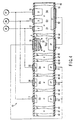
- FIG. 4 is a sectional view showing a surge protection semiconductor device according to the third embodiment of the present invention.
- the same reference numerals as in FIG. 1 denote the same parts.
- a thyristor element Thy1 and first to sixth diode elements D1 to D6 are provided as a vertical element structure in consideration of the surge withstand voltage and the like.
- an n - -type semiconductor substrate 11 is separated by a p + -type isolation region 40 to provide an n - -type element region 50 for forming the thyristor element Thy1 and an n - -type element region 51 for forming the first, second, and sixth diode elements D1, D2, and D6.
- the element region 50 includes an anode region formed from the second surface, an n-type buried layer 32 formed from the first surface and having an impurity concentration higher than that of the semiconductor substrate, a p-type base region, and a plurality of n + -type emitter layers.
- the element region 51 includes anode regions of the first, second, and sixth diode elements D1, D2, and D6 formed from the first surface, and a common cathode region formed from the second surface.
- a common cathode electrode 52 formed in the common cathode region is connected to an anode electrode 14 of the thyristor element Thy1, thereby providing a diode bridge shown in FIG. 2 as in the above embodiments.
- the rest is the same as in FIG. 1.
- the isolation region 47 made of the n - -type semiconductor substrate is interposed between the n - -type element region 50 and the n - -type element region 43, thereby doubly isolating the n - -type element region 50 and n - -type element region 43 by the p + -type isolation region 40, the n - -type isolation region 47, and the p + -type isolation region 40.
- This increases the breakdown voltage between the thyristor element Thy1 and diode element D4, and improves the reliability of the diode bridge.
- a method of setting the forward breakdown voltage of the thyristor element Thy1 lower than the breakdown voltage of the first to sixth diode elements D1, D2, D3, D4, D5, and D6 a method of making the p-type base diffusion depth of the thyristor element smaller than the p-type anode diffusion depth of the diode elements may also be used instead of the method using the buried-structure thyristor element Thy1 having the buried diffusion layer 32 as described above.
- the breakdown voltage of the thyristor Thy1 must be, e.g., 230 V, 290 V, 310 V, or 350 V, although this voltage is determined by the buried layer 32, and the diode withstand voltage must be higher than that, e.g., 800 V.
- the thyristor element Thy1 and diode elements D1, D2, D3, D4, D5, and D6 are formed into a monolithic structure on the same semiconductor chip, and the diode elements D1 and D4 are isolated by a double isolation structure. Accordingly, a compact surge protection semiconductor device having a high breakdown voltage and high reliability can be obtained.
Landscapes
- Thyristors (AREA)
- Semiconductor Integrated Circuits (AREA)
- Emergency Protection Circuit Devices (AREA)
- Metal-Oxide And Bipolar Metal-Oxide Semiconductor Integrated Circuits (AREA)
Abstract
Description
In this manner, a monolithic surge protection semiconductor device in which the balanced surge protection circuit is formed on a single substrate is obtained.
Opposite-polarity surge is:
Claims (7)
- A surge protection semiconductor device comprising:a semiconductor substrate of a first conductivity type having first and second surfaces;a thyristor element, provided in a first semiconductor region of a second conductivity type formed in the semiconductor substrate so as to extend from the first surface to the second surface, having an anode electrode and cathode electrode;a substrate region of the first conductivity type, the substrate region being adjacent to one side of the first semiconductor region and being comprised of the semiconductor substrate;first and second diode elements provided in a second semiconductor region of the first conductivity type, the second semiconductor region being adjacent to the other side of the first semiconductor region and being comprised of the semiconductor substrate, each of the first and second diode elements having an anode electrode and a common cathode electrode;third, fourth and fifth diode elements each being provided in third, fourth and fifth semiconductor regions, respectively, the third, fourth and fifth semiconductor regions being comprised of the semiconductor substrate and being isolated from each other by one of isolation regions of the second conductivity type, one of the isolation regions being adjacent to the substrate region, and each of the third, fourth and fifth diode elements having an anode electrode and cathode electrode formed on the first surface; anda sixth diode element provided in a sixth semiconductor region of the first conductivity type adjacent to the second substrate region and isolated by one of the isolation regions, the sixth semiconductor region being comprised of the semiconductor substrate, the sixth diode element having an anode electrode and cathode electrode.
- The surge protection semiconductor device according to claim 1, wherein the second surface is covered with an insulating film.
- The surge protection semiconductor device according to claim 1, wherein each of the thyristor element and first to sixth diode elements has a lateral structure in which the anode and cathode electrodes are provided on the first surface.
- The surge protection semiconductor device according to claim 1, wherein at least the first, second and sixth diode elements have a vertical structure in which the anode electrodes are provided on the first surface, and the cathode electrodes are provided on the second surface, and the thyristor element has a vertical structure in which the cathode electrode is provided on the first surface, and the anode electrode is provided on the second surface.
- The surge protection semiconductor device according to claim 1, wherein the anode electrode of the first diode element and the cathode electrode of the fourth diode element are connected, the cathode electrode of the first diode element and the cathode electrode of the second diode element are connected, the anode electrode of the second diode element and the cathode electrode of the fifth diode element are connected, the anode electrode of the fifth diode element and the anode electrode of the fourth diode element are connected, the thyristor element is connected between a first node, given by the cathode electrode of the first diode element and the cathode electrode of the second diode element, and a second node, given by the anode electrode of the fifth diode element and the anode electrode of the fourth diode element such that the first node is positive with respect to the second node, the cathode electrode of the sixth diode element is connected to the first node, the anode electrode of the third diode element is connected to the second node, and the anode electrode of the sixth diode element and the cathode electrode of the third diode element are connected to a ground terminal.
- The surge protection semiconductor device according to claim 3, wherein first and second electrode terminals are connected to both a third node, given by the anode electrode of the first diode element and the cathode electrode of the fourth diode element, and a fourth node, given by the anode electrode of the second diode element and the cathode electrode of the fifth diode element, respectively, and also connected to a circuit to be protected.
- A surge protection semiconductor device according to claim 1, wherein a forward breakdown voltage of the thyristor element is set lower than a breakdown voltage of the first to sixth diode elements.
Applications Claiming Priority (3)
| Application Number | Priority Date | Filing Date | Title |
|---|---|---|---|
| JP2001342236 | 2001-11-07 | ||
| JP2001342236 | 2001-11-07 | ||
| PCT/JP2002/011578 WO2003041170A1 (en) | 2001-11-07 | 2002-11-06 | Surge protection semiconductor device |
Publications (2)
| Publication Number | Publication Date |
|---|---|
| EP1453094A1 true EP1453094A1 (en) | 2004-09-01 |
| EP1453094A4 EP1453094A4 (en) | 2006-08-23 |
Family
ID=19156126
Family Applications (1)
| Application Number | Title | Priority Date | Filing Date |
|---|---|---|---|
| EP02780027A Ceased EP1453094A4 (en) | 2001-11-07 | 2002-11-06 | SEMICONDUCTOR DEVICE FOR PROTECTION AGAINST OVERVOLTAGE |
Country Status (5)
| Country | Link |
|---|---|
| US (1) | US6870202B2 (en) |
| EP (1) | EP1453094A4 (en) |
| JP (1) | JP4369230B2 (en) |
| CN (1) | CN1321457C (en) |
| WO (1) | WO2003041170A1 (en) |
Cited By (2)
| Publication number | Priority date | Publication date | Assignee | Title |
|---|---|---|---|---|
| WO2014008415A1 (en) | 2012-07-05 | 2014-01-09 | Littelfuse, Inc. | Crowbar device for voltage transient circuit protection |
| CN105023953A (en) * | 2015-07-10 | 2015-11-04 | 淄博汉林半导体有限公司 | Vertical field effect diode and manufacture method thereof |
Families Citing this family (56)
| Publication number | Priority date | Publication date | Assignee | Title |
|---|---|---|---|---|
| US7189610B2 (en) * | 2004-10-18 | 2007-03-13 | Semiconductor Components Industries, L.L.C. | Semiconductor diode and method therefor |
| US7622753B2 (en) * | 2005-08-31 | 2009-11-24 | Stmicroelectronics S.A. | Ignition circuit |
| US7515391B2 (en) * | 2005-10-19 | 2009-04-07 | Littlefuse, Inc. | Linear low capacitance overvoltage protection circuit |
| US7489488B2 (en) * | 2005-10-19 | 2009-02-10 | Littelfuse, Inc. | Integrated circuit providing overvoltage protection for low voltage lines |
| US7538409B2 (en) * | 2006-06-07 | 2009-05-26 | International Business Machines Corporation | Semiconductor devices |
| US7508643B2 (en) * | 2006-10-27 | 2009-03-24 | Manitowoc Crane Companies, Inc. | System for overvoltage suppression for construction equipment |
| KR101532424B1 (en) * | 2008-09-12 | 2015-07-01 | 페어차일드코리아반도체 주식회사 | Electrostatic discharge diode |
| CN101640414B (en) * | 2009-08-26 | 2011-06-15 | 苏州晶讯科技股份有限公司 | Programmable semiconductor anti-surge protective device with deep trap structure |
| US9520486B2 (en) | 2009-11-04 | 2016-12-13 | Analog Devices, Inc. | Electrostatic protection device |
| US8513722B2 (en) | 2010-03-02 | 2013-08-20 | Micron Technology, Inc. | Floating body cell structures, devices including same, and methods for forming same |
| US9646869B2 (en) | 2010-03-02 | 2017-05-09 | Micron Technology, Inc. | Semiconductor devices including a diode structure over a conductive strap and methods of forming such semiconductor devices |
| US8288795B2 (en) | 2010-03-02 | 2012-10-16 | Micron Technology, Inc. | Thyristor based memory cells, devices and systems including the same and methods for forming the same |
| US9608119B2 (en) * | 2010-03-02 | 2017-03-28 | Micron Technology, Inc. | Semiconductor-metal-on-insulator structures, methods of forming such structures, and semiconductor devices including such structures |
| US8507966B2 (en) | 2010-03-02 | 2013-08-13 | Micron Technology, Inc. | Semiconductor cells, arrays, devices and systems having a buried conductive line and methods for forming the same |
| US8432651B2 (en) | 2010-06-09 | 2013-04-30 | Analog Devices, Inc. | Apparatus and method for electronic systems reliability |
| US10199482B2 (en) | 2010-11-29 | 2019-02-05 | Analog Devices, Inc. | Apparatus for electrostatic discharge protection |
| CN102569289A (en) * | 2010-12-23 | 2012-07-11 | 中芯国际集成电路制造(上海)有限公司 | Structure and method for eliminating process antenna effect |
| US8598621B2 (en) | 2011-02-11 | 2013-12-03 | Micron Technology, Inc. | Memory cells, memory arrays, methods of forming memory cells, and methods of forming a shared doped semiconductor region of a vertically oriented thyristor and a vertically oriented access transistor |
| US8592860B2 (en) | 2011-02-11 | 2013-11-26 | Analog Devices, Inc. | Apparatus and method for protection of electronic circuits operating under high stress conditions |
| US8952418B2 (en) | 2011-03-01 | 2015-02-10 | Micron Technology, Inc. | Gated bipolar junction transistors |
| US8519431B2 (en) | 2011-03-08 | 2013-08-27 | Micron Technology, Inc. | Thyristors |
| US8772848B2 (en) | 2011-07-26 | 2014-07-08 | Micron Technology, Inc. | Circuit structures, memory circuitry, and methods |
| US8680620B2 (en) | 2011-08-04 | 2014-03-25 | Analog Devices, Inc. | Bi-directional blocking voltage protection devices and methods of forming the same |
| US8947841B2 (en) | 2012-02-13 | 2015-02-03 | Analog Devices, Inc. | Protection systems for integrated circuits and methods of forming the same |
| US8829570B2 (en) | 2012-03-09 | 2014-09-09 | Analog Devices, Inc. | Switching device for heterojunction integrated circuits and methods of forming the same |
| US8946822B2 (en) | 2012-03-19 | 2015-02-03 | Analog Devices, Inc. | Apparatus and method for protection of precision mixed-signal electronic circuits |
| US8637899B2 (en) * | 2012-06-08 | 2014-01-28 | Analog Devices, Inc. | Method and apparatus for protection and high voltage isolation of low voltage communication interface terminals |
| US8796729B2 (en) | 2012-11-20 | 2014-08-05 | Analog Devices, Inc. | Junction-isolated blocking voltage devices with integrated protection structures and methods of forming the same |
| US9123540B2 (en) | 2013-01-30 | 2015-09-01 | Analog Devices, Inc. | Apparatus for high speed signal processing interface |
| US9006781B2 (en) | 2012-12-19 | 2015-04-14 | Analog Devices, Inc. | Devices for monolithic data conversion interface protection and methods of forming the same |
| US8860080B2 (en) | 2012-12-19 | 2014-10-14 | Analog Devices, Inc. | Interface protection device with integrated supply clamp and method of forming the same |
| US9275991B2 (en) | 2013-02-13 | 2016-03-01 | Analog Devices, Inc. | Apparatus for transceiver signal isolation and voltage clamp |
| US9147677B2 (en) | 2013-05-16 | 2015-09-29 | Analog Devices Global | Dual-tub junction-isolated voltage clamp devices for protecting low voltage circuitry connected between high voltage interface pins and methods of forming the same |
| US9171832B2 (en) | 2013-05-24 | 2015-10-27 | Analog Devices, Inc. | Analog switch with high bipolar blocking voltage in low voltage CMOS process |
| EP2863432A1 (en) | 2013-10-21 | 2015-04-22 | Nxp B.V. | ESD protection device |
| US9673054B2 (en) | 2014-08-18 | 2017-06-06 | Micron Technology, Inc. | Array of gated devices and methods of forming an array of gated devices |
| US9224738B1 (en) | 2014-08-18 | 2015-12-29 | Micron Technology, Inc. | Methods of forming an array of gated devices |
| US9209187B1 (en) | 2014-08-18 | 2015-12-08 | Micron Technology, Inc. | Methods of forming an array of gated devices |
| US9484739B2 (en) | 2014-09-25 | 2016-11-01 | Analog Devices Global | Overvoltage protection device and method |
| US9478608B2 (en) | 2014-11-18 | 2016-10-25 | Analog Devices, Inc. | Apparatus and methods for transceiver interface overvoltage clamping |
| US10068894B2 (en) | 2015-01-12 | 2018-09-04 | Analog Devices, Inc. | Low leakage bidirectional clamps and methods of forming the same |
| US10181719B2 (en) | 2015-03-16 | 2019-01-15 | Analog Devices Global | Overvoltage blocking protection device |
| US9673187B2 (en) | 2015-04-07 | 2017-06-06 | Analog Devices, Inc. | High speed interface protection apparatus |
| CN104900645B (en) * | 2015-05-28 | 2019-01-11 | 北京燕东微电子有限公司 | Voltage surge protector part and its manufacturing method |
| FR3039014B1 (en) * | 2015-07-13 | 2019-06-14 | Stmicroelectronics (Tours) Sas | TELEPHONE LINE PROTECTION AGAINST OVERVOLTAGES |
| US9831233B2 (en) | 2016-04-29 | 2017-11-28 | Analog Devices Global | Apparatuses for communication systems transceiver interfaces |
| US10734806B2 (en) | 2016-07-21 | 2020-08-04 | Analog Devices, Inc. | High voltage clamps with transient activation and activation release control |
| US10249609B2 (en) | 2017-08-10 | 2019-04-02 | Analog Devices, Inc. | Apparatuses for communication systems transceiver interfaces |
| CN108364947A (en) * | 2018-02-02 | 2018-08-03 | 苏州晶讯科技股份有限公司 | A kind of semiconductor voltage device of surge protector |
| US10700056B2 (en) | 2018-09-07 | 2020-06-30 | Analog Devices, Inc. | Apparatus for automotive and communication systems transceiver interfaces |
| US11387648B2 (en) | 2019-01-10 | 2022-07-12 | Analog Devices International Unlimited Company | Electrical overstress protection with low leakage current for high voltage tolerant high speed interfaces |
| JP7294594B2 (en) | 2019-06-03 | 2023-06-20 | リテルヒューズ・セミコンダクター・(ウーシー)・カンパニー・リミテッド | Integrated multi-device chips and packages |
| US11362083B2 (en) * | 2020-02-11 | 2022-06-14 | Semtech Corporation | TVS diode circuit with high energy dissipation and linear capacitance |
| CN111668211B (en) * | 2020-07-13 | 2024-11-26 | 北京时代华诺科技有限公司 | A semiconductor structure, surge protection device and manufacturing method |
| US11948933B2 (en) * | 2022-02-09 | 2024-04-02 | Semiconductor Components Industries, Llc | Semiconductor devices and methods of manufacturing semiconductor devices |
| CN115346979B (en) * | 2022-10-18 | 2023-02-21 | 富芯微电子有限公司 | TVS device based on thyristor structure and manufacturing method thereof |
Family Cites Families (16)
| Publication number | Priority date | Publication date | Assignee | Title |
|---|---|---|---|---|
| JPS4643937B1 (en) * | 1968-02-26 | 1971-12-27 | ||
| JPS5127985B2 (en) * | 1971-10-01 | 1976-08-16 | ||
| US4644437A (en) * | 1985-11-01 | 1987-02-17 | At&T Bell Laboratories | Telephone subscriber loop overvoltage protection integrated circuit |
| FR2670339B1 (en) * | 1990-12-07 | 1993-03-12 | Sgs Thomson Microelectronics | PROTECTION CIRCUIT LIMITING OVERVOLTAGES BETWEEN TWO SELECTED LIMITS AND ITS MONOLITHIC INTEGRATION. |
| US5493469A (en) * | 1991-01-18 | 1996-02-20 | Mildred A. Lace | Surge protection for data lines |
| JP3083881B2 (en) * | 1991-07-30 | 2000-09-04 | 新電元工業株式会社 | Surge protection element |
| US5369291A (en) * | 1993-03-29 | 1994-11-29 | Sunpower Corporation | Voltage controlled thyristor |
| US5512784A (en) * | 1994-04-19 | 1996-04-30 | Jerrold Communications, General Instrument Corporation | Surge protector semiconductor subassembly for 3-lead transistor aotline package |
| FR2719721B1 (en) * | 1994-05-09 | 1996-09-20 | Sgs Thomson Microelectronics | Telephone line interface protection. |
| FR2729008B1 (en) * | 1994-12-30 | 1997-03-21 | Sgs Thomson Microelectronics | INTEGRATED POWER CIRCUIT |
| JPH097729A (en) * | 1995-06-16 | 1997-01-10 | Shinko Electric Ind Co Ltd | Semiconductor arresters and combination type arresters |
| KR100240872B1 (en) * | 1997-02-17 | 2000-01-15 | 윤종용 | Electrostatic discharge circuit and integrated circuit having the same |
| US6104591A (en) * | 1998-03-09 | 2000-08-15 | Teccor Electronics, Inc. | Telephone line protection element |
| FR2783353A1 (en) * | 1998-09-16 | 2000-03-17 | St Microelectronics Sa | INSULATION WALL BETWEEN POWER COMPONENTS |
| FR2800513B1 (en) * | 1999-11-03 | 2002-03-29 | St Microelectronics Sa | POWER COMPONENT STATE DETECTOR |
| FR2808621B1 (en) * | 2000-05-05 | 2002-07-19 | St Microelectronics Sa | SINGLE CONTROL MONOLITHIC COMPONENT FOR A MIXED BRIDGE |
-
2002
- 2002-11-06 CN CNB028219392A patent/CN1321457C/en not_active Expired - Fee Related
- 2002-11-06 WO PCT/JP2002/011578 patent/WO2003041170A1/en not_active Ceased
- 2002-11-06 EP EP02780027A patent/EP1453094A4/en not_active Ceased
- 2002-11-06 JP JP2003543104A patent/JP4369230B2/en not_active Expired - Fee Related
-
2004
- 2004-04-30 US US10/835,062 patent/US6870202B2/en not_active Expired - Fee Related
Cited By (6)
| Publication number | Priority date | Publication date | Assignee | Title |
|---|---|---|---|---|
| WO2014008415A1 (en) | 2012-07-05 | 2014-01-09 | Littelfuse, Inc. | Crowbar device for voltage transient circuit protection |
| CN104412339A (en) * | 2012-07-05 | 2015-03-11 | 保险丝公司 | Crowbar device for voltage transient circuit protection |
| EP2870611A4 (en) * | 2012-07-05 | 2015-11-25 | Littelfuse Inc | VOLTAGE LIMITATION DEVICE FOR TRANSIENT OVERVOLTAGE CIRCUIT PROTECTION |
| CN104412339B (en) * | 2012-07-05 | 2017-10-17 | 保险丝公司 | Crow bar device for voltage transient circuit protection |
| US10074642B2 (en) | 2012-07-05 | 2018-09-11 | Littelfuse, Inc. | Crowbar device for voltage transient circuit protection |
| CN105023953A (en) * | 2015-07-10 | 2015-11-04 | 淄博汉林半导体有限公司 | Vertical field effect diode and manufacture method thereof |
Also Published As
| Publication number | Publication date |
|---|---|
| JP4369230B2 (en) | 2009-11-18 |
| CN1321457C (en) | 2007-06-13 |
| JPWO2003041170A1 (en) | 2005-03-03 |
| CN1582497A (en) | 2005-02-16 |
| EP1453094A4 (en) | 2006-08-23 |
| US20040201035A1 (en) | 2004-10-14 |
| WO2003041170A1 (en) | 2003-05-15 |
| US6870202B2 (en) | 2005-03-22 |
Similar Documents
| Publication | Publication Date | Title |
|---|---|---|
| US6870202B2 (en) | Surge protection semiconductor device | |
| US11456596B2 (en) | USB type-C load switch ESD protection | |
| US7019338B1 (en) | Subscriber interface protection circuit | |
| EP0412561B1 (en) | Semiconductor integrated circuit device | |
| US8111495B2 (en) | Low forward voltage drop transient voltage suppressor and method of fabricating | |
| KR100517770B1 (en) | Electrostatic Discharge Protection Element | |
| JP5249768B2 (en) | Integrated circuit for protecting low voltage lines from overvoltage | |
| US20130285196A1 (en) | Esd protection circuit providing multiple protection levels | |
| US5898193A (en) | Electrostatic discharge protecting circuit formed in a minimized area | |
| US6987300B2 (en) | High voltage ESD-protection structure | |
| JPH10303409A (en) | Protection components for telephone line interfaces | |
| EP0822596A2 (en) | Improvements in or relating to integrated circuits | |
| US5138413A (en) | Piso electrostatic discharge protection device | |
| JPH0282533A (en) | bipolar transistor | |
| US6384453B1 (en) | High withstand voltage diode and method for manufacturing same | |
| JP2791067B2 (en) | Monolithic overvoltage protection assembly | |
| JP4369231B2 (en) | Surge protection semiconductor device | |
| JP2611639B2 (en) | Semiconductor device | |
| TWI239626B (en) | Structure of electrostatic discharge suppressor and method of stacking package with semiconductor devices | |
| JP2003110119A (en) | Electrostatic surge protection element | |
| US10916536B2 (en) | ESD protection device for a MEMS element | |
| JPH0729974A (en) | Semiconductor device | |
| JPH0629466A (en) | Semiconductor integrated circuit | |
| JPH0358468A (en) | Semiconductor integrated circuit device | |
| JPH05211292A (en) | Semiconductor input protection device |
Legal Events
| Date | Code | Title | Description |
|---|---|---|---|
| PUAI | Public reference made under article 153(3) epc to a published international application that has entered the european phase |
Free format text: ORIGINAL CODE: 0009012 |
|
| 17P | Request for examination filed |
Effective date: 20040511 |
|
| AK | Designated contracting states |
Kind code of ref document: A1 Designated state(s): AT BE BG CH CY CZ DE DK EE ES FI FR GB GR IE IT LI LU MC NL PT SE SK TR |
|
| AX | Request for extension of the european patent |
Extension state: AL LT LV MK RO SI |
|
| A4 | Supplementary search report drawn up and despatched |
Effective date: 20060726 |
|
| REG | Reference to a national code |
Ref country code: DE Ref legal event code: 8566 |
|
| 17Q | First examination report despatched |
Effective date: 20061128 |
|
| 17Q | First examination report despatched |
Effective date: 20061128 |
|
| STAA | Information on the status of an ep patent application or granted ep patent |
Free format text: STATUS: THE APPLICATION HAS BEEN REFUSED |
|
| 18R | Application refused |
Effective date: 20080310 |