EP1445843A1 - Ansteuerschaltung und Verfahren zum Betreiben eines Halbleiterlasers - Google Patents
Ansteuerschaltung und Verfahren zum Betreiben eines Halbleiterlasers Download PDFInfo
- Publication number
- EP1445843A1 EP1445843A1 EP03360020A EP03360020A EP1445843A1 EP 1445843 A1 EP1445843 A1 EP 1445843A1 EP 03360020 A EP03360020 A EP 03360020A EP 03360020 A EP03360020 A EP 03360020A EP 1445843 A1 EP1445843 A1 EP 1445843A1
- Authority
- EP
- European Patent Office
- Prior art keywords
- circuit
- semiconductor laser
- differential amplifier
- vcsel
- connection
- Prior art date
- Legal status (The legal status is an assumption and is not a legal conclusion. Google has not performed a legal analysis and makes no representation as to the accuracy of the status listed.)
- Granted
Links
- 238000000034 method Methods 0.000 title claims abstract description 11
- 239000004065 semiconductor Substances 0.000 title claims description 45
- 239000003990 capacitor Substances 0.000 claims description 10
- 230000007257 malfunction Effects 0.000 claims description 3
- 238000004519 manufacturing process Methods 0.000 description 3
- 230000006978 adaptation Effects 0.000 description 2
- 230000005540 biological transmission Effects 0.000 description 2
- 238000011156 evaluation Methods 0.000 description 2
- 238000005259 measurement Methods 0.000 description 2
- 238000011144 upstream manufacturing Methods 0.000 description 2
- 230000008878 coupling Effects 0.000 description 1
- 238000010168 coupling process Methods 0.000 description 1
- 238000005859 coupling reaction Methods 0.000 description 1
- 230000007613 environmental effect Effects 0.000 description 1
- 230000006870 function Effects 0.000 description 1
- 230000003287 optical effect Effects 0.000 description 1
- 238000000206 photolithography Methods 0.000 description 1
- 230000001960 triggered effect Effects 0.000 description 1
- 235000012431 wafers Nutrition 0.000 description 1
Images

Classifications
-
- H—ELECTRICITY
- H01—ELECTRIC ELEMENTS
- H01S—DEVICES USING THE PROCESS OF LIGHT AMPLIFICATION BY STIMULATED EMISSION OF RADIATION [LASER] TO AMPLIFY OR GENERATE LIGHT; DEVICES USING STIMULATED EMISSION OF ELECTROMAGNETIC RADIATION IN WAVE RANGES OTHER THAN OPTICAL
- H01S5/00—Semiconductor lasers
- H01S5/04—Processes or apparatus for excitation, e.g. pumping, e.g. by electron beams
- H01S5/042—Electrical excitation ; Circuits therefor
-
- H—ELECTRICITY
- H01—ELECTRIC ELEMENTS
- H01S—DEVICES USING THE PROCESS OF LIGHT AMPLIFICATION BY STIMULATED EMISSION OF RADIATION [LASER] TO AMPLIFY OR GENERATE LIGHT; DEVICES USING STIMULATED EMISSION OF ELECTROMAGNETIC RADIATION IN WAVE RANGES OTHER THAN OPTICAL
- H01S5/00—Semiconductor lasers
- H01S5/10—Construction or shape of the optical resonator, e.g. extended or external cavity, coupled cavities, bent-guide, varying width, thickness or composition of the active region
- H01S5/18—Surface-emitting [SE] lasers, e.g. having both horizontal and vertical cavities
- H01S5/183—Surface-emitting [SE] lasers, e.g. having both horizontal and vertical cavities having only vertical cavities, e.g. vertical cavity surface-emitting lasers [VCSEL]
Definitions
- the present invention relates to a control circuit for and a Method for operating a semiconductor laser, in particular a vertical Cavity Surface Emitting Laser (VCSEL).
- VCSEL vertical Cavity Surface Emitting Laser
- the control circuit according to the invention is particularly suitable for the Control of different types of VCSEL, i.e. VCSEL with different characteristics.
- VCSEL are semiconductor laser diodes that emit their light vertically to the surface of the Emit wafers. These have compared to other semiconductor lasers many advantages. The very high ones are worth mentioning, for example Modulation rates, the very low power consumption, a high one Efficiency for optical coupling with light guides, as well geometries defined by photolithography. VCSELs are also very good inexpensive. The cost factor is compared to DFB lasers for example about 100. VCSELs have a limited number, however Output power and a strong temperature dependence. Areas of application for VCSEL are, for example, 10 Gbit Ethernet networks, In-office systems but also transmission systems in the short-haul area like metro networks. VCSELs with a have long been known Laser wavelength in the range of 850 nm. Recently, too VCSEL sold with a laser wavelength of 1300 nm. In contrast to DFB lasers, which are usually operated in continuous wave mode and whose laser light for message transmission via an external downstream modulator is modulated, VCSEL are direct modulated.
- a circuit for controlling a VCSEL with 850 nm is known Emission wavelength, which is a differential amplifier. There is one Connection of the VCSEL to ground and the other connection of the VCSEL to connected to an output of the differential amplifier. Such Wiring is also referred to as "single-ended".
- the VCSEL is operated directly modulated.
- VCSEL with an emission wavelength of 850 nm have a relatively high Threshold voltage of approx. 1.8 V, a threshold current of approx. 3 mA and a limit current of approx. 10 mA.
- Their differential resistance is in of the order of 60 ⁇ .
- the Connection line between control circuit and VCSEL chip usually adapted to the differential resistance of the VCSEL.
- the recently developed VCSELs with an emission wavelength of 1300 nm have a threshold voltage of 1.3 V, but a differential resistance of the order of 120 ⁇ .
- the use of connecting cables with an impedance of 55 - 85 ⁇ is unproblematic from a technical and economic point of view.
- the control circuit of the prior art described above has the disadvantage that it can be used - if at all only to a limited extent - for VCSELs with a high differential resistance.
- the invention has for its object to provide a circuit and a method for driving a semiconductor with which a semiconductor laser with high differential resistance is driven directly modulated.
- the invention is also based on the object of a circuit and a To create procedures that are also used for the control of Semiconductor lasers with lower differential resistance can be used.
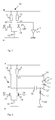
- Figure 1 shows schematically a control circuit of the prior art for direct modulation of a semiconductor laser, especially in form a semiconductor laser diode.
- Numeral 1 denotes a vertical Cavitiy Surface Emitting Laser (VCSEL), its cathode on ground is switched, the modulation of the VCSEL via the anode connection he follows.
- the circuit of the prior art represents a known one Differential amplifier 10 represents the VCSEL 1 for direct modulation is connected upstream.
- the differential amplifier 10 is a symmetrical one DC amplifier with two inputs E1, E2 and two outputs A1, A2.
- the differential amplifier comprises two resistors 11, 12, two Transistors 13, 14 and a constant current source 15, which in the common emitter line of the transistors 13, 14 is arranged.
- Differential amplifiers are generally known to the person skilled in the art and need them therefore not explained here. Because of their low Differential amplifiers are then preferably also temperature drift used when no voltage difference but only one Input voltage should be amplified. In this case, one of the ground both inputs E1 or E2. In the circuit of FIG. 1 input E1 is connected to ground and control of VCSEL 1 takes place via input E2 and output A1, which is connected to the anode of the VCSEL 1 is connected. Output A1 is not switched. As in Figure 1 the VCSEL 1 is shown on one side via a connection, namely the anode driven while the cathode is connected to ground. Such Wiring is also referred to as "single-ended".
- FIG. 2 shows a schematic representation of a first embodiment of a driver or control circuit according to the invention for a VCSEL 1, the VCSEL 1 being controlled differentially.
- the circuit according to the invention is preferably designed as an integrated circuit (IC) or part of an integrated circuit. The circuit according to the invention is explained in more detail below.
- the driver circuit according to the invention of FIG. 2 also includes the differential amplifier 10, but both inputs E1 and E2 and both outputs A1 and A2 are used for the differential control of the VCSEL 1.
- the transistors 13, 14 are shown as bipolar transistors. It is obvious to a person skilled in the art that a differential amplifier with MOSFET transistors can also be used.
- the output A2 is connected to the anode 1a of the VCSEL 1 and the output A1 via a capacitor 16 to the cathode 1b of the VCSEL 1. Between the capacitor 16 and the cathode 1b of the VCSEL 1 there are also a coil 17 and a resistor 18 in series as a direct current path switched to ground.
- the VCSEL 1 is operated differentially, ie the resistors 11, 12 and the current source 15 are determined in such a way that a voltage difference of approximately 1.5 V drops at the VCSEL 1 and modulation frequencies are applied via the inputs E1 and E2.
- the cathode of the VCSEL 1 is AC-coupled (AC-coupled) to the output A2 of the differential amplifier 10 via the capacitor 16.
- the circuit branch output A1 of the differential amplifier 10, anode 1a or cathode 1b of the VCSEL 1 is DC-coupled via the coil 17 and the resistor 18 (DC-coupled).
- the bias voltage for operating the VCSEL 10 is applied via this branch.
- the VCSEL 1 is connected to the circuit via impedance-matched connecting lines 26 and 27.
- the control circuit according to the invention is particularly advantageous for the Control of a VCSEL with high differential resistance.
- the VCSEL with a Emission wavelengths of 850 nm have a relatively high threshold voltage of about 1.8 V, a threshold current of about 3 mA and one Limit current of approx. 10 mA.
- Their differential resistance is in the Order of magnitude of 60 ⁇ . Because of the strong temperature dependence VCSEL strives to provide the integrated circuit that Control circuit includes, and the chip with the VCSEL spatially to be spaced apart. The distances are usually in Centimeter range.
- the connecting line of the control circuit to VCSEL chip is usually like this to avoid distortion designed that the characteristic impedance is complete, i.e. this is on adjusted the differential resistance of the VCSEL. interconnectors with an impedance of 55 to 85 ⁇ are under economic Aspects feasible and available with reasonable effort.
- the recently developed VCSEL with an emission wavelength of 1300 nm have a threshold voltage of 1.3 V, but a differential Resistance in the order of 120 ⁇ . interconnectors with an impedance of 120 ⁇ are in production and Handling technically complex and therefore not inexpensive.
- control circuit according to the invention with differential Control can also be used for VCSEL with high differential resistance Wave resistance of the control / connecting lines in a simple manner and Way to be completed.
- the differential control can also be concluded in this case simple technical means, i.e. the available lines with a line impedance in the range of 50 to 85 ⁇ can be used become.
- the circuit according to the invention of FIG. 2 also has the advantage on that the capacitor 16, the coil 17 and the resistor 18, the also be referred to as Bias-T due to the selected circuit arrangement - namely the use of a DC-coupled and one AC-coupled branches for connecting the VCSEL - such are dimensioned so that these on the IC that the drive circuit includes, can be integrated.
- the order of magnitude shows Capacitor 16 a value of 2 pF, the coil 17 a value of 4.7 nH and the resistance has a value of 50 ⁇ .
- the circuit according to the invention thus has the advantage that the VCSEL only in the "high frequency” range is operated differentially, while in DC range for applying the bias voltage of the VCSEL "quasi" “single-ended” is controlled.
- the circuit according to the invention also has the advantage that it also for the known VCSEL with lower differential resistance can be used.
- the circuit or is not only suitable for the Control of a VCSEL with higher differential resistance, so for example a VCSEL with 1300 nm emission wavelength and differential resistance of approximately 120 ⁇ , as previously described, but can also be simple for those who have been around for a long time known VCSEL with 850 nm emission wavelength and with lower Resistance of approx. 60 ⁇ can be used.
- a 850 nm VCSEL only becomes an input, i.e. E1 or E2 to a constant one Potential and the cathode of the VCSEL does not have the capacitor 16 connected to output A2, but simply connected to ground, whereby a "single-ended" control of the VCSEL is achieved.
- Figure 3 shows an advantageous embodiment of the invention Circuit of Figure 2. For reasons of symmetry are between output A1 and capacitor 16 a coil 19 and two diodes 20, 21 via one Resistor 22 connected in series to ground. That way it is achieved that the working points are the same on both sides, whereby Distortions can be avoided.
- Figure 4 shows a further advantageous embodiment of the Driver circuit according to the invention of Figure 3.
- the transistors 23, 24 and 25 shown in Figure 4 are MOSFET transistors.
- the circuit shown for the resistors enables variable adjustment of the working point in an advantageous manner of the differential amplifier 10 by corresponding voltages applied to the gate of transistors 23, 24 and 25.
- a driver circuit according to the invention designed in this way is suitable especially for an automatic adjustment or coordination of the Control circuit to the VCSEL 1 used in each case.
- This coordination can be done in terms of various factors and desirable be, for example, for the use of the circuit with VCSEL, which at emit different wavelengths of laser light.
- the characteristics or characteristic curves usually differ significantly from each other, so that a strong adjustment is required in this case.
- the vote can be particularly with regard to the Using the circuit in the "single-ended" mode or the differential mode or “dual-ended” mode.
- the automatic adjustment / tuning of the circuit can also continue intended to compensate for less significant deviations e.g. when using identical or similar VCSEL different Manufacturer or for the compensation of manufacturing tolerances certain VCSEL.
- automatic tuning can also the adaptation to different environmental influences during the Operation of the VCSEL, e.g. Influences of temperature. Depending on Desired purpose is therefore a correspondingly large To provide tuning range and a corresponding tuning accuracy.
- the constant current source 15 (not shown) digital-to-analog converter intended. That way you can Settings / adjustments of the circuit or the control of the Semiconductor laser means executed on a microprocessor Program.
- the microprocessor together Input / output modules and memory (RAM, ROM etc.) can be external provided or be on the IC of the drive circuit.
- the circuit comprises at least the (not shown) microprocessor for executing a program for Control of the semiconductor laser and / or adjustment of the circuit.
- the procedure for automatically adapting the control circuit to the respectively connected VCSEL is described in more detail below.
- the control current is provided as an example as the starting value or parameter for setting the circuit. However, other parameters, such as voltage, temperature etc., can be used instead of or in addition to the setting.
- the circuit is preferably measured during commissioning or the characteristic of the VCSEL is measured and the circuit is set on the basis of the measurement data obtained. For this purpose, the circuit is connected to the previously described (not shown) microprocessor, which executes a program for acquiring the characteristic of the VCSEL.
- the microprocessor is connected via corresponding input / output modules and digital-to-analog converters to the inputs E1, E2 of transistors 13 and 14, to a control input of constant current source 15 and to the gate inputs of transistors 23, 24 and 25 ,
- the output of a monitor diode which is usually present on a semiconductor laser, for example VCSEL, is made available to the microprocessor for evaluation via an analog-to-digital converter.
- Appropriate sensors and interfaces can be provided to record further characteristic data, for example the temperature.
- the characteristic of the VCSEL is preferably measured first.
- control circuit namely by step-by-step setting of suitable current / voltage values, equidistant steps or, depending on the characteristic curve range, variable step sizes also being possible.
- the determined characteristic curves can be saved, for example for later evaluation, for logging, etc.
- the maximum control current is set and the emission rate is measured by means of the monitor diode.
- the maximum control current is gradually reduced and the current for the desired emission rate is determined with the monitor diode.
- the operating point determined in this way is saved and the circuit is fixed to this setting.
- the characteristics of certain semiconductor lasers can already be stored in a memory, so that the characteristic can not be determined.
- the tuning of the driver circuit can also be done by different events can be controlled, e.g. the initial start-up, changing a semiconductor laser, e.g. of a VCSEL, the number the hours of operation, the occurrence of a malfunction, etc. Also can have certain configurations of the driver / driver circuit in the memory for certain types of semiconductor lasers and / or Operating modes (dual-ended, single-ended) must be stored. Depending on The requirement is then none or only a quick one Fine tuning necessary. It can also be provided that the Operation of the semiconductor laser continuously monitored or in short Time intervals measurement data of the semiconductor laser can be evaluated, so to ensure largely optimized operation of the semiconductor laser.
Landscapes
- Physics & Mathematics (AREA)
- Condensed Matter Physics & Semiconductors (AREA)
- General Physics & Mathematics (AREA)
- Electromagnetism (AREA)
- Optics & Photonics (AREA)
- Semiconductor Lasers (AREA)
Abstract
Description
Demgegenüber liegt der Erfindung die Aufgabe zugrunde, eine Schaltung und ein Verfahren zur Ansteuerung eines Halbleiters zu schaffen, mit der ein Halbleiterlaser mit hohem differentiellen Widerstand direkt moduliert angesteuert wird.
Die erfindungsgemäße Treiberschaltung der Figur 2 umfasst ebenfalls den Differenzverstärker 10, wobei jedoch beide Eingänge E1 und E2 und beide Ausgänge A1 und A2 zur differentiellen Ansteuerung des VCSEL 1 verwendet werden. Die Transistoren 13, 14 sind als bipolare Transistoren dargestellt. Für den Fachmann ist es offensichtlich, dass auch ein Differenzverstärker mit MOSFET-Transistoren verwendet werden kann. Der Ausgang A2 ist mit der Anode 1a des VCSEL 1 verbunden und der Ausgang A1 über einen Kondensator 16 mit der Kathode 1b des VCSEL 1. Zwischen Kondensator 16 und Kathode 1b des VCSEL 1 sind noch eine Spule 17 und ein Widerstand 18 in Reihe als Gleichstrompfad gegen Masse geschaltet. Der VCSEL 1 wird differentiell betrieben, d.h. die Widerstände 11 , 12 und die Stromquelle 15 sind so bestimmt, dass am VCSEL 1 eine Spannungsdifferenz von circa 1,5 V abfällt und über die Eingänge E1 und E2 werden Modulationsfrequenzen angelegt. Die Kathode des VCSEL 1 ist über den Kondensator 16 mit dem Ausgang A2 des Differenzverstärkers 10 wechselstromgekoppelt (AC-gekoppelt). Der Schaltungszweig Ausgang A1 des Differenzverstärkers 10, Anode 1a bzw. Kathode 1b des VCSEL 1 ist über die Spule 17 und den Widerstand 18 gleichstromgekoppelt (DCgekoppelt). Über diesen Zweig wird die Vorspannung zum Betreiben des VCSEL 10 aufgebracht wird. Der VCSEL 1 ist über impedanzangepasste Anschlussleitungen 26 und 27 mit der Schaltung verbunden.
Gemäß dem Verfahren werden
- mittels der Schaltung zunächst Kennliniendaten des Halbleiterlasers gemessen,
- aus den gemessenen Daten zumindest ein Startwerte der Schaltung ermittelt und eingestellt und
- durch Variation des Startwertes zumindest in Abhängigkeit von einer gewünschte Kenngröße, z.B. der Emissionsrate, des Halbleiterlasers Betriebswerte der Schaltung zum Betreiben der Schaltung mit diesem Halbleiterlaser ermittelt und eingestellt.
Zur Einstellung/Anpassung der Schaltung wird vorzugsweise zunächst die Kennlinie des VCSEL gemessen. Dieses geschieht mit der Ansteuerschaltung, und zwar durch schrittweise Einstellung von geeigneten Stroms-/Spannungswerten, wobei äquidistante Schritte oder je nach Kennlinienbereich auch variable Schrittweiten vorgesehen sein können. Die ermittelten Kennlinien könne abgespeichert werden, z.B. zur späteren Auswertung, zur Protokollierung etc. Anschließend wird der maximale Steuerstrom eingestellt und die Emissionsrate mittels der Monitordiode gemessen. Dann wird die maximale Steuerstrom schrittweise erniedrigt und dabei der Strom für die gewünschte Emissionsrate mit der Monitordiode ermittelt. Der so ermittelte Arbeitspunkt wird abgespeichert und die Schaltungin auf diese Einstellung fixiert. Je nach den jeweiligen Anforderungen (Toleranzwerte etc.) können für bestimmte Halbleiterlaser auch deren Kennlinien bereits in einen Speicher hinterlegt sein, so dass auf eine Ermittlung der Kennlinie verzichtet werden kann.
Claims (10)
- Schaltung zur Ansteuerung eines Halbleiterlasers (1), insbesondere eines Vertical Cavitiy Surface Emitting Laser (VCSEL), mit einem Differenzverstärker (10) zur direkten Ansteuerung des Halbleiterlaser (1), dadurch gekennzeichnet , dass mittels des Differenzverstärkers (10) ein an die Schaltung anzuschließender Halbleiterlaser (1) differential angesteuert ist, wobei ein erster Ausgang (A1) des Differenzverstärkers (10) mit einem ersten Anschluss (1a) des Halbleiterlaser (1) gleichstromgekoppelt und ein zweiter Ausgang (A2) des Differenzverstärkers (10) mit einem zweiten Anschluss (1b) des Halbleiterlaser (1) wechselstromgekoppelt verbunden ist.
- Schaltung nach Anspruch 1, dadurch gekennzeichnet, dass der zweite Ausgang (A2) des Differenzverstärkers (10) mit dem zweiten Anschluss (1b) des Halbleiterlaser (1) mittels eines Kondensators (16) verbunden ist, wobei zwischen Kondensator (16) und zweitem Anschluss (1b) eine Spule (17) und ein Widerstand (18) in Reihe gegen Masse geschaltet sind.
- Schaltung nach Anspruch 1 oder 2, dadurch gekennzeichnet, dass den Widerständen (11, 12) des Differenzverstärkers (10) einstellbare Widerstände (24, 25) parallel geschaltet sind.
- Schaltung nach einem der Ansprüche 1 bis 3, dadurch gekennzeichnet, dass zwischen dem zweiten Ausgang (A2) des Differenzverstärkers (10) und dem Kondensator (16) eine Reihenschaltung von einer weiteren Spule (19), zweier Dioden (20, 21) und eines weiteren Widerstands (22) gegen Masse vorgesehen ist.
- Schaltung nach einem der Ansprüche 1 bis 4, dadurch gekennzeichnet, dass Digital-zu-Analog-Wandler zumindest für die Eingänge (E1, E2) des Differenzverstärkers (10) und eines Steuereinganges der Konstantstromquelle (15) vorgesehen sind.
- Schaltung nach Anspruch 5, dadurch gekennzeichnet, dass die Schaltung einen Mikroprozessor zur Ausführung eines Programms zur Ansteuerung des Halbleiterlaser (1) und/oder Einstellung der Schaltung umfasst.
- Schaltung nach einem der Ansprüche 1 bis 5, dadurch gekennzeichnet, dass die Schaltung den Halbleiterlaser (1) umfasst, der insbesondere eine Halbleiterdiode ist, wobei die Anode der Laserdiode den ersten Anschluss (1a) des Halbleiterlasers (1) und die Kathode der Laserdiode den zweiten Anschluss (1b) des Halbleiterlasers (1) darstellt.
- Schaltung nach Anspruch 7, dadurch gekennzeichnet, dass die Schaltung und der Halbleiterlaser (1) auf räumlich getrennten Integrierten Schaltungen angeordnet sind, wobei impedanzangepasste Leitungen (26, 27) der Schaltung zum Anschließen des Halbleiterlaser (1) an die Schaltung vorgesehen sind.
- Verfahren zum Betreiben einer Schaltung nach einem der Ansprüche 1 bis 8, dadurch gekennzeichnet, dass von vorgegebenen Ereignissen gesteuert die Schaltung an den verwendeten Halbleiterlaser (1) angepasst wird,wobei mittels der Schaltung zunächst Kennliniendaten des Halbleiterlasers (1) gemessen werden,aus den gemessenen Daten zumindest ein Startwerte der Schaltung ermittelt und eingestellt werden unddurch Variation des Startwertes zumindest in Abhängigkeit von einer gewünschte Kenngröße des Halbleiterlasers Betriebswerte der Schaltung zum Betreiben der Schaltung mit diesem Halbleiterlaser (1) ermittelt und eingestellt werden.
- Verfahren nach Anspruch 8, dadurch gekennzeichnet, dass zumindest eine erstmalige oder erneute Inbetriebnahme, ein Austausch des Halbleiterlasers (1), eine vorgegebene Anzahl von Betriebsstunden oder ein Auftreten einer Fehlfunktion ein Ereignis im Sinne der vorgegebenen Ereignisse darstellt.
Priority Applications (5)
| Application Number | Priority Date | Filing Date | Title |
|---|---|---|---|
| DE50305106T DE50305106D1 (de) | 2003-02-05 | 2003-02-05 | Ansteuerschaltung und Verfahren zum Betreiben eines Halbleiterlasers |
| AT03360020T ATE340425T1 (de) | 2003-02-05 | 2003-02-05 | Ansteuerschaltung und verfahren zum betreiben eines halbleiterlasers |
| EP03360020A EP1445843B1 (de) | 2003-02-05 | 2003-02-05 | Ansteuerschaltung und Verfahren zum Betreiben eines Halbleiterlasers |
| US10/760,397 US7502400B2 (en) | 2003-02-05 | 2004-01-21 | Drive circuit and method of operating a semiconductor laser |
| CN200410000496.9A CN1275369C (zh) | 2003-02-05 | 2004-02-04 | 操作半导体激光器的驱动电路和方法 |
Applications Claiming Priority (1)
| Application Number | Priority Date | Filing Date | Title |
|---|---|---|---|
| EP03360020A EP1445843B1 (de) | 2003-02-05 | 2003-02-05 | Ansteuerschaltung und Verfahren zum Betreiben eines Halbleiterlasers |
Publications (2)
| Publication Number | Publication Date |
|---|---|
| EP1445843A1 true EP1445843A1 (de) | 2004-08-11 |
| EP1445843B1 EP1445843B1 (de) | 2006-09-20 |
Family
ID=32605461
Family Applications (1)
| Application Number | Title | Priority Date | Filing Date |
|---|---|---|---|
| EP03360020A Expired - Lifetime EP1445843B1 (de) | 2003-02-05 | 2003-02-05 | Ansteuerschaltung und Verfahren zum Betreiben eines Halbleiterlasers |
Country Status (5)
| Country | Link |
|---|---|
| US (1) | US7502400B2 (de) |
| EP (1) | EP1445843B1 (de) |
| CN (1) | CN1275369C (de) |
| AT (1) | ATE340425T1 (de) |
| DE (1) | DE50305106D1 (de) |
Cited By (2)
| Publication number | Priority date | Publication date | Assignee | Title |
|---|---|---|---|---|
| EP2112727A1 (de) * | 2008-04-25 | 2009-10-28 | JDS Uniphase Corporation | Gleichstromgekoppelter Antrieb mit aktiver Terminierung |
| US8228962B2 (en) | 2009-01-23 | 2012-07-24 | Iptronics A/S | Low power drive circuit |
Families Citing this family (16)
| Publication number | Priority date | Publication date | Assignee | Title |
|---|---|---|---|---|
| US7411986B2 (en) * | 2004-03-25 | 2008-08-12 | Finisar Corporation | Optical system laser driver with a built in output inductor for improved frequency response |
| CN100546134C (zh) * | 2005-06-01 | 2009-09-30 | 佳能株式会社 | 激光器驱动电路 |
| JP5035054B2 (ja) * | 2008-03-19 | 2012-09-26 | 住友電気工業株式会社 | 半導体レーザ駆動回路 |
| CN102064468B (zh) * | 2010-12-15 | 2012-08-22 | 烽火通信科技股份有限公司 | 一种低电压自适应光通信激光驱动器电路 |
| US10097908B2 (en) * | 2014-12-31 | 2018-10-09 | Macom Technology Solutions Holdings, Inc. | DC-coupled laser driver with AC-coupled termination element |
| JP6046288B1 (ja) * | 2016-01-14 | 2016-12-14 | 株式会社東芝 | 電流出力回路及び光送信器 |
| US10630052B2 (en) | 2017-10-04 | 2020-04-21 | Macom Technology Solutions Holdings, Inc. | Efficiency improved driver for laser diode in optical communication |
| CN108683065B (zh) * | 2018-03-29 | 2024-01-19 | 昂纳科技(深圳)集团股份有限公司 | 一种激光装置 |
| EP3804247B1 (de) | 2018-05-30 | 2024-08-14 | MACOM Technology Solutions Holdings, Inc. | Integrierte schaltungsbasierte wechselstrom-kopplungstopologie |
| US11005573B2 (en) | 2018-11-20 | 2021-05-11 | Macom Technology Solutions Holdings, Inc. | Optic signal receiver with dynamic control |
| CN111029897B (zh) * | 2019-11-29 | 2020-12-29 | 长飞光纤光缆股份有限公司 | 一种vcsel阳极驱动电路及方法 |
| US12013423B2 (en) | 2020-09-30 | 2024-06-18 | Macom Technology Solutions Holdings, Inc. | TIA bandwidth testing system and method |
| US11658630B2 (en) | 2020-12-04 | 2023-05-23 | Macom Technology Solutions Holdings, Inc. | Single servo loop controlling an automatic gain control and current sourcing mechanism |
| CN115220160B (zh) * | 2022-06-30 | 2023-10-27 | 青岛海信宽带多媒体技术有限公司 | 一种光模块 |
| US12567847B2 (en) | 2022-12-27 | 2026-03-03 | Macom Technology Solutions Holdings, Inc. | Variable gain optical modulator with open collector driver amplifier and method of operation |
| US12395130B2 (en) | 2022-12-27 | 2025-08-19 | Macom Technology Solutions Holdings, Inc. | Variable gain optical modulator with open collector driver amplifier and method of operation |
Citations (5)
| Publication number | Priority date | Publication date | Assignee | Title |
|---|---|---|---|---|
| JPH10145221A (ja) * | 1996-11-14 | 1998-05-29 | Toshiba Corp | 出力回路装置 |
| JPH11233876A (ja) * | 1998-02-16 | 1999-08-27 | Sumitomo Electric Ind Ltd | レーザモジュール |
| JP2000031760A (ja) * | 1998-07-07 | 2000-01-28 | Matsushita Electric Ind Co Ltd | 増幅器 |
| US20020085599A1 (en) * | 2000-12-29 | 2002-07-04 | Karl Schrodinger | Electronic driver circuit for directly modulated semiconductor lasers |
| EP1261082A1 (de) * | 2001-05-25 | 2002-11-27 | Agilent Technologies, Inc. (a Delaware corporation) | Optoelektronische Schaltung und Kontrollschaltung |
Family Cites Families (8)
| Publication number | Priority date | Publication date | Assignee | Title |
|---|---|---|---|---|
| CA1210070A (en) * | 1984-10-26 | 1986-08-19 | Northern Telecom Limited | Laser transmitter |
| JP3432620B2 (ja) * | 1994-12-20 | 2003-08-04 | 富士通株式会社 | 光送信機及びレーザダイオードモジュール |
| US5883910A (en) * | 1997-07-03 | 1999-03-16 | Maxim Integrated Products, Inc. | High speed semiconductor laser driver circuits |
| JP3492891B2 (ja) * | 1997-09-19 | 2004-02-03 | 株式会社東芝 | 出力回路装置 |
| US6226322B1 (en) * | 1998-03-30 | 2001-05-01 | Texas Instruments Incorporated | Analog receive equalizer for digital-subscriber-line communications system |
| EP1289081A1 (de) * | 2001-09-03 | 2003-03-05 | Agilent Technologies, Inc. (a Delaware corporation) | Lasertreiberschaltung und Verfahren zum Treiben eines Lasers |
| WO2003036770A2 (de) * | 2001-09-14 | 2003-05-01 | Infineon Technologies Ag | Integrierter schaltkreis zur ansteuerung einer laserdiode |
| US6792019B2 (en) * | 2002-02-28 | 2004-09-14 | Texas Instruments Incorporated | Driver with tail currents in discrete subranges |
-
2003
- 2003-02-05 EP EP03360020A patent/EP1445843B1/de not_active Expired - Lifetime
- 2003-02-05 AT AT03360020T patent/ATE340425T1/de not_active IP Right Cessation
- 2003-02-05 DE DE50305106T patent/DE50305106D1/de not_active Expired - Lifetime
-
2004
- 2004-01-21 US US10/760,397 patent/US7502400B2/en not_active Expired - Fee Related
- 2004-02-04 CN CN200410000496.9A patent/CN1275369C/zh not_active Expired - Fee Related
Patent Citations (5)
| Publication number | Priority date | Publication date | Assignee | Title |
|---|---|---|---|---|
| JPH10145221A (ja) * | 1996-11-14 | 1998-05-29 | Toshiba Corp | 出力回路装置 |
| JPH11233876A (ja) * | 1998-02-16 | 1999-08-27 | Sumitomo Electric Ind Ltd | レーザモジュール |
| JP2000031760A (ja) * | 1998-07-07 | 2000-01-28 | Matsushita Electric Ind Co Ltd | 増幅器 |
| US20020085599A1 (en) * | 2000-12-29 | 2002-07-04 | Karl Schrodinger | Electronic driver circuit for directly modulated semiconductor lasers |
| EP1261082A1 (de) * | 2001-05-25 | 2002-11-27 | Agilent Technologies, Inc. (a Delaware corporation) | Optoelektronische Schaltung und Kontrollschaltung |
Non-Patent Citations (3)
| Title |
|---|
| PATENT ABSTRACTS OF JAPAN vol. 1998, no. 10 31 August 1998 (1998-08-31) * |
| PATENT ABSTRACTS OF JAPAN vol. 1999, no. 13 30 November 1999 (1999-11-30) * |
| PATENT ABSTRACTS OF JAPAN vol. 2000, no. 04 31 August 2000 (2000-08-31) * |
Cited By (3)
| Publication number | Priority date | Publication date | Assignee | Title |
|---|---|---|---|---|
| EP2112727A1 (de) * | 2008-04-25 | 2009-10-28 | JDS Uniphase Corporation | Gleichstromgekoppelter Antrieb mit aktiver Terminierung |
| US8009709B2 (en) | 2008-04-25 | 2011-08-30 | Jds Uniphase Corporation | DC coupled driver with active termination |
| US8228962B2 (en) | 2009-01-23 | 2012-07-24 | Iptronics A/S | Low power drive circuit |
Also Published As
| Publication number | Publication date |
|---|---|
| US20050276290A1 (en) | 2005-12-15 |
| DE50305106D1 (de) | 2006-11-02 |
| CN1519994A (zh) | 2004-08-11 |
| ATE340425T1 (de) | 2006-10-15 |
| EP1445843B1 (de) | 2006-09-20 |
| US7502400B2 (en) | 2009-03-10 |
| CN1275369C (zh) | 2006-09-13 |
Similar Documents
| Publication | Publication Date | Title |
|---|---|---|
| EP1445843B1 (de) | Ansteuerschaltung und Verfahren zum Betreiben eines Halbleiterlasers | |
| EP0134960B1 (de) | Schaltungsanordnung zur Ansteuerung von Halbleiterlasern | |
| DE2902789C2 (de) | ||
| DE3044956A1 (de) | "digitaler hochleistungsverstaerker" | |
| EP0075295A2 (de) | Optisches Übertragungssystem für hochfrequente digitale Signale | |
| DE69225589T2 (de) | Vorverstärker | |
| DE1948851A1 (de) | Signaluebertragungsschaltung,insbesondere Phasenteilerschaltung | |
| EP3552280B1 (de) | Laseranordnung und verfahren zum herstellen einer laseranordnung | |
| DE4001064A1 (de) | Rauscharmer hochgeschwindigkeitsdifferentialverstaerker und verfahren zum erzielen einer rauscharmen hochgeschwindigkeitsverstaerkung eines differentialeingangssignales | |
| EP0562359B1 (de) | Ansteuerschaltung für eine Laserdiode | |
| DE3832448A1 (de) | Messverstaerker mit programmierbarer verstaerkung | |
| EP1725078A1 (de) | Treiberschaltung für elektronische Bauteile | |
| DE3508034C2 (de) | ||
| DE69610591T2 (de) | Optischer Halbleitermodulator und Treiberschaltung | |
| DE3411303C2 (de) | ||
| DE3317027A1 (de) | Schaltungsanordnung zur umwandlung eines elektrischen einganssignales in ein optisches ausgangssignal | |
| DE3715238A1 (de) | Transistor-schalteinrichtung mit basisstrom-regulierung | |
| DE102016223314A1 (de) | Treiberschaltung, insbesondere für eine Pockelszelle und Verfahren zum Betrieb einer Treiberschaltung | |
| DE69710506T2 (de) | Array-Anordnung mit Schaltkreisen und Konstantstromquellen für eine Vielzahl von Kanälen | |
| DE60312157T2 (de) | Techniken zur vorspannung von lasern | |
| EP0598855B1 (de) | Optisch steuerbarer halbleiterlaser | |
| EP1425831B1 (de) | Integrierter schaltkreis zur ansteuerung einer laserdiode | |
| DE69303306T2 (de) | Optischer Verstärker mit verbesserter Linearität | |
| DE3503942C2 (de) | ||
| DE4030995C2 (de) |
Legal Events
| Date | Code | Title | Description |
|---|---|---|---|
| PUAI | Public reference made under article 153(3) epc to a published international application that has entered the european phase |
Free format text: ORIGINAL CODE: 0009012 |
|
| 17P | Request for examination filed |
Effective date: 20040302 |
|
| AK | Designated contracting states |
Kind code of ref document: A1 Designated state(s): AT BE BG CH CY CZ DE DK EE ES FI FR GB GR HU IE IT LI LU MC NL PT SE SI SK TR |
|
| AX | Request for extension of the european patent |
Extension state: AL LT LV MK RO |
|
| AKX | Designation fees paid |
Designated state(s): AT BE BG CH CY CZ DE DK EE ES FI FR GB GR HU IE IT LI LU MC NL PT SE SI SK TR |
|
| GRAP | Despatch of communication of intention to grant a patent |
Free format text: ORIGINAL CODE: EPIDOSNIGR1 |
|
| GRAS | Grant fee paid |
Free format text: ORIGINAL CODE: EPIDOSNIGR3 |
|
| GRAA | (expected) grant |
Free format text: ORIGINAL CODE: 0009210 |
|
| AK | Designated contracting states |
Kind code of ref document: B1 Designated state(s): AT BE BG CH CY CZ DE DK EE ES FI FR GB GR HU IE IT LI LU MC NL PT SE SI SK TR |
|
| PG25 | Lapsed in a contracting state [announced via postgrant information from national office to epo] |
Ref country code: CZ Free format text: LAPSE BECAUSE OF FAILURE TO SUBMIT A TRANSLATION OF THE DESCRIPTION OR TO PAY THE FEE WITHIN THE PRESCRIBED TIME-LIMIT Effective date: 20060920 Ref country code: SK Free format text: LAPSE BECAUSE OF FAILURE TO SUBMIT A TRANSLATION OF THE DESCRIPTION OR TO PAY THE FEE WITHIN THE PRESCRIBED TIME-LIMIT Effective date: 20060920 Ref country code: NL Free format text: LAPSE BECAUSE OF FAILURE TO SUBMIT A TRANSLATION OF THE DESCRIPTION OR TO PAY THE FEE WITHIN THE PRESCRIBED TIME-LIMIT Effective date: 20060920 Ref country code: FI Free format text: LAPSE BECAUSE OF FAILURE TO SUBMIT A TRANSLATION OF THE DESCRIPTION OR TO PAY THE FEE WITHIN THE PRESCRIBED TIME-LIMIT Effective date: 20060920 Ref country code: SI Free format text: LAPSE BECAUSE OF FAILURE TO SUBMIT A TRANSLATION OF THE DESCRIPTION OR TO PAY THE FEE WITHIN THE PRESCRIBED TIME-LIMIT Effective date: 20060920 Ref country code: IE Free format text: LAPSE BECAUSE OF FAILURE TO SUBMIT A TRANSLATION OF THE DESCRIPTION OR TO PAY THE FEE WITHIN THE PRESCRIBED TIME-LIMIT Effective date: 20060920 Ref country code: IT Free format text: LAPSE BECAUSE OF FAILURE TO SUBMIT A TRANSLATION OF THE DESCRIPTION OR TO PAY THE FEE WITHIN THE PRESCRIBED TIME-LIMIT;WARNING: LAPSES OF ITALIAN PATENTS WITH EFFECTIVE DATE BEFORE 2007 MAY HAVE OCCURRED AT ANY TIME BEFORE 2007. THE CORRECT EFFECTIVE DATE MAY BE DIFFERENT FROM THE ONE RECORDED. Effective date: 20060920 |
|
| REG | Reference to a national code |
Ref country code: GB Ref legal event code: FG4D Free format text: NOT ENGLISH |
|
| REG | Reference to a national code |
Ref country code: CH Ref legal event code: EP |
|
| REG | Reference to a national code |
Ref country code: IE Ref legal event code: FG4D Free format text: LANGUAGE OF EP DOCUMENT: GERMAN |
|
| REF | Corresponds to: |
Ref document number: 50305106 Country of ref document: DE Date of ref document: 20061102 Kind code of ref document: P |
|
| GBT | Gb: translation of ep patent filed (gb section 77(6)(a)/1977) |
Effective date: 20061016 |
|
| PG25 | Lapsed in a contracting state [announced via postgrant information from national office to epo] |
Ref country code: DK Free format text: LAPSE BECAUSE OF FAILURE TO SUBMIT A TRANSLATION OF THE DESCRIPTION OR TO PAY THE FEE WITHIN THE PRESCRIBED TIME-LIMIT Effective date: 20061220 Ref country code: BG Free format text: LAPSE BECAUSE OF FAILURE TO SUBMIT A TRANSLATION OF THE DESCRIPTION OR TO PAY THE FEE WITHIN THE PRESCRIBED TIME-LIMIT Effective date: 20061220 Ref country code: SE Free format text: LAPSE BECAUSE OF FAILURE TO SUBMIT A TRANSLATION OF THE DESCRIPTION OR TO PAY THE FEE WITHIN THE PRESCRIBED TIME-LIMIT Effective date: 20061220 |
|
| PG25 | Lapsed in a contracting state [announced via postgrant information from national office to epo] |
Ref country code: ES Free format text: LAPSE BECAUSE OF FAILURE TO SUBMIT A TRANSLATION OF THE DESCRIPTION OR TO PAY THE FEE WITHIN THE PRESCRIBED TIME-LIMIT Effective date: 20061231 |
|
| PG25 | Lapsed in a contracting state [announced via postgrant information from national office to epo] |
Ref country code: CH Free format text: LAPSE BECAUSE OF NON-PAYMENT OF DUE FEES Effective date: 20070228 Ref country code: LI Free format text: LAPSE BECAUSE OF NON-PAYMENT OF DUE FEES Effective date: 20070228 Ref country code: MC Free format text: LAPSE BECAUSE OF NON-PAYMENT OF DUE FEES Effective date: 20070228 |
|
| NLV1 | Nl: lapsed or annulled due to failure to fulfill the requirements of art. 29p and 29m of the patents act | ||
| PG25 | Lapsed in a contracting state [announced via postgrant information from national office to epo] |
Ref country code: PT Free format text: LAPSE BECAUSE OF FAILURE TO SUBMIT A TRANSLATION OF THE DESCRIPTION OR TO PAY THE FEE WITHIN THE PRESCRIBED TIME-LIMIT Effective date: 20070312 |
|
| RAP2 | Party data changed (patent owner data changed or rights of a patent transferred) |
Owner name: ALCATEL LUCENT |
|
| ET | Fr: translation filed | ||
| REG | Reference to a national code |
Ref country code: IE Ref legal event code: FD4D |
|
| PLBE | No opposition filed within time limit |
Free format text: ORIGINAL CODE: 0009261 |
|
| STAA | Information on the status of an ep patent application or granted ep patent |
Free format text: STATUS: NO OPPOSITION FILED WITHIN TIME LIMIT |
|
| 26N | No opposition filed |
Effective date: 20070621 |
|
| REG | Reference to a national code |
Ref country code: CH Ref legal event code: PL |
|
| BERE | Be: lapsed |
Owner name: ALCATEL Effective date: 20070228 |
|
| PG25 | Lapsed in a contracting state [announced via postgrant information from national office to epo] |
Ref country code: BE Free format text: LAPSE BECAUSE OF NON-PAYMENT OF DUE FEES Effective date: 20070228 |
|
| PG25 | Lapsed in a contracting state [announced via postgrant information from national office to epo] |
Ref country code: GR Free format text: LAPSE BECAUSE OF FAILURE TO SUBMIT A TRANSLATION OF THE DESCRIPTION OR TO PAY THE FEE WITHIN THE PRESCRIBED TIME-LIMIT Effective date: 20061221 |
|
| PG25 | Lapsed in a contracting state [announced via postgrant information from national office to epo] |
Ref country code: AT Free format text: LAPSE BECAUSE OF NON-PAYMENT OF DUE FEES Effective date: 20070205 |
|
| PG25 | Lapsed in a contracting state [announced via postgrant information from national office to epo] |
Ref country code: EE Free format text: LAPSE BECAUSE OF FAILURE TO SUBMIT A TRANSLATION OF THE DESCRIPTION OR TO PAY THE FEE WITHIN THE PRESCRIBED TIME-LIMIT Effective date: 20060920 |
|
| PG25 | Lapsed in a contracting state [announced via postgrant information from national office to epo] |
Ref country code: LU Free format text: LAPSE BECAUSE OF NON-PAYMENT OF DUE FEES Effective date: 20070205 Ref country code: CY Free format text: LAPSE BECAUSE OF FAILURE TO SUBMIT A TRANSLATION OF THE DESCRIPTION OR TO PAY THE FEE WITHIN THE PRESCRIBED TIME-LIMIT Effective date: 20060920 |
|
| PG25 | Lapsed in a contracting state [announced via postgrant information from national office to epo] |
Ref country code: HU Free format text: LAPSE BECAUSE OF FAILURE TO SUBMIT A TRANSLATION OF THE DESCRIPTION OR TO PAY THE FEE WITHIN THE PRESCRIBED TIME-LIMIT Effective date: 20070321 Ref country code: TR Free format text: LAPSE BECAUSE OF FAILURE TO SUBMIT A TRANSLATION OF THE DESCRIPTION OR TO PAY THE FEE WITHIN THE PRESCRIBED TIME-LIMIT Effective date: 20060920 |
|
| REG | Reference to a national code |
Ref country code: FR Ref legal event code: GC Effective date: 20140717 |
|
| REG | Reference to a national code |
Ref country code: FR Ref legal event code: PLFP Year of fee payment: 13 |
|
| REG | Reference to a national code |
Ref country code: FR Ref legal event code: CA Effective date: 20150521 |
|
| REG | Reference to a national code |
Ref country code: FR Ref legal event code: CA Effective date: 20150521 |
|
| REG | Reference to a national code |
Ref country code: FR Ref legal event code: PLFP Year of fee payment: 14 |
|
| REG | Reference to a national code |
Ref country code: FR Ref legal event code: PLFP Year of fee payment: 15 |
|
| REG | Reference to a national code |
Ref country code: FR Ref legal event code: PLFP Year of fee payment: 16 |
|
| PGFP | Annual fee paid to national office [announced via postgrant information from national office to epo] |
Ref country code: GB Payment date: 20200129 Year of fee payment: 18 Ref country code: DE Payment date: 20200121 Year of fee payment: 18 |
|
| PGFP | Annual fee paid to national office [announced via postgrant information from national office to epo] |
Ref country code: FR Payment date: 20200113 Year of fee payment: 18 |
|
| REG | Reference to a national code |
Ref country code: DE Ref legal event code: R119 Ref document number: 50305106 Country of ref document: DE |
|
| GBPC | Gb: european patent ceased through non-payment of renewal fee |
Effective date: 20210205 |
|
| PG25 | Lapsed in a contracting state [announced via postgrant information from national office to epo] |
Ref country code: GB Free format text: LAPSE BECAUSE OF NON-PAYMENT OF DUE FEES Effective date: 20210205 Ref country code: FR Free format text: LAPSE BECAUSE OF NON-PAYMENT OF DUE FEES Effective date: 20210228 Ref country code: DE Free format text: LAPSE BECAUSE OF NON-PAYMENT OF DUE FEES Effective date: 20210901 |